EP0802402A1 - Elément récepteur pyroélectrique pour l'infrarouge et détecteur d'infrarouge l'utilisant - Google Patents
Elément récepteur pyroélectrique pour l'infrarouge et détecteur d'infrarouge l'utilisant Download PDFInfo
- Publication number
- EP0802402A1 EP0802402A1 EP97106200A EP97106200A EP0802402A1 EP 0802402 A1 EP0802402 A1 EP 0802402A1 EP 97106200 A EP97106200 A EP 97106200A EP 97106200 A EP97106200 A EP 97106200A EP 0802402 A1 EP0802402 A1 EP 0802402A1
- Authority
- EP
- European Patent Office
- Prior art keywords
- receiving element
- pyroelectric
- substrate
- type
- patch
- Prior art date
- Legal status (The legal status is an assumption and is not a legal conclusion. Google has not performed a legal analysis and makes no representation as to the accuracy of the status listed.)
- Granted
Links
Images







Classifications
-
- G—PHYSICS
- G01—MEASURING; TESTING
- G01J—MEASUREMENT OF INTENSITY, VELOCITY, SPECTRAL CONTENT, POLARISATION, PHASE OR PULSE CHARACTERISTICS OF INFRARED, VISIBLE OR ULTRAVIOLET LIGHT; COLORIMETRY; RADIATION PYROMETRY
- G01J1/00—Photometry, e.g. photographic exposure meter
- G01J1/02—Details
-
- G—PHYSICS
- G01—MEASURING; TESTING
- G01J—MEASUREMENT OF INTENSITY, VELOCITY, SPECTRAL CONTENT, POLARISATION, PHASE OR PULSE CHARACTERISTICS OF INFRARED, VISIBLE OR ULTRAVIOLET LIGHT; COLORIMETRY; RADIATION PYROMETRY
- G01J5/00—Radiation pyrometry, e.g. infrared or optical thermometry
- G01J5/10—Radiation pyrometry, e.g. infrared or optical thermometry using electric radiation detectors
- G01J5/34—Radiation pyrometry, e.g. infrared or optical thermometry using electric radiation detectors using capacitors, e.g. pyroelectric capacitors
-
- H—ELECTRICITY
- H10—SEMICONDUCTOR DEVICES; ELECTRIC SOLID-STATE DEVICES NOT OTHERWISE PROVIDED FOR
- H10N—ELECTRIC SOLID-STATE DEVICES NOT OTHERWISE PROVIDED FOR
- H10N10/00—Thermoelectric devices comprising a junction of dissimilar materials, i.e. devices exhibiting Seebeck or Peltier effects
Definitions
- the present invention relates to a pyroelectric-type IR receiving element for receiving infrared (IR) rays radiated from an object, and an improved IR sensor using the same receiving element.
- IR infrared
- Pyroelectric-type IR receiving elements are used to sensors for detecting a moving object such as human.
- a pyroelectric-type IR sensor is shown in FIG. 26.
- the IR sensor comprises an IR receiving element 100 that is generally known as a dual-type receiving element, a circuit board 120 to which the receiving element is fixed, a base 130 having three output pins 131 projecting therefrom downwardly, and a package cover 140 having an IR transmittable window 141 .
- the receiving element 100 comprises a substrate 101 made of a pyroelectric material, a pair of first and second electrodes ( 102a , 103a ) formed on a top surface of the substrate, and a pair of third and fourth electrodes ( 102b , 103b ) formed on a bottom surface of the substrate, and a pair of positive and negative output terminals 104 and 105 formed on both of the top and bottom surfaces at opposite ends of the substrate.
- the substrate 101 is made of a ceramic material such as PBTiO 3 or PZT, a single crystal such as LiTaO 3 , or a high molecular compound such as PVF 2 .
- the four electrodes are made of an IR absorbent material such as NiCr or the like, and have a same rectangular shape.
- the first and second electrodes ( 102a , 103a ) are arranged such that a longitudinal side of the first electrode extends parallel to that of the second electrode.
- the third and fourth electrodes ( 102b , 103b ) are arranged so as to be respectively overlapped with the first and second electrodes ( 102a , 103a ) through the substrate 101 .
- the first and fourth electrodes ( 102a , 103b ) are connected to the positive output terminal 104 by conductive patterns 106 .
- the second and third electrodes ( 103a , 102b ) are connected to the negative output terminal 105 by conductive patterns 107 .
- a pair of IR receiving portions 102 and 103 are defined on the pyroelectric substrate 101 .
- the IR receiving portions 102 and 103 receive IR rays
- the received IR rays are converted to a heat energy so that electric charges are generated.
- a voltage-difference signal is obtained from the IR receiving element 100 through a field-effect transistor (FET) 123 and a high resistance element 124 , as shown in FIG. 27C.
- FET field-effect transistor
- the receiving element 100 is fixed to a pair of stands 121 formed on the circuit board 120 in a bridge fashion.
- the circuit board 120 mounting thereon the receiving element 100 is attached to the base 130 , and then covered by the package cover 140 .
- a thermal-insulation property of the pyroelectric substrate 101 is improved, and a thin pyroelectric substrate having a thickness of 40 to 100 ⁇ m is used in the past.
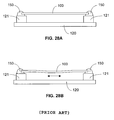
- the IR receiving element 100 having such a thin thickness is fixed on the stands 121 in the bridge fashion by a conductive bond 150 , as shown in FIG.
- a thermal stress resulting from a difference of thermal expansion coefficients between the pyroelectric substrate 101 and the stand material 121 or the conductive bond 150 is applied to the pyroelectric substrate by a temperature change of the circumference even when no IR ray strike the IR receiving element 100 , as shown by a two-way arrow of FIG. 28B.
- the thermal stress tends to concentrate at defect portions, chipping portions, or micro-cracks in the pyroelectric substrate. This stress concentration brings about the occurrence of undesired electric charges. As a result, there causes a problem that unexpected noise signals generally known as a popcorn noise are output from the IR receiving element.
- a concern of the present invention is to provide an improved pyroelectric-type IR receiving element capable of reducing the occurrence of popcorn noise while maintaining good IR sensitivity. That is, a pyroelectric material is used as a substrate. The substrate is fixed to a supporting body at its support ends. At least one patch having a substantially rectangular shape is formed in the substrate. The patch is formed on its opposite surfaces with first and second electrodes which are overlapped to each other so as to develop a voltage difference between the first and second electrodes when one of the first and second electrodes receives an IR ray.
- the substrate has a U-shaped slit composed of a pair of side slits and a base slit connecting the side slits.
- the U-shaped slit surrounds continuously three sides of the patch, so that the patch is supported by the substrate in a cantilever fashion at a cantilever end which is opposed to one of the support ends of the substrate.
- a stress concentration to be considered is not developed in the patch, so that the occurrence of popcorn noise can be reduced.
- both ends of the U-shaped slit are bent toward the inside of the U-shaped slit to obtain a neck portion at the cantilever end.
- both ends of the U-shaped slit are formed with rounded holes having a diameter larger than its slit width to obtain a neck portion at the cantilever end.
- the U-shaped slit is formed in a horseshoe-shaped slit.
- a pyroelectric-type IR sensor using the IR receiving element of the present invention comprises a three-dimensional circuit block on which the IR receiving element is mounted, and a package for incorporating the circuit block therein.
- the circuit block is provided with a pair of stands formed on a top surface of the circuit block. The support ends of the IR receiving element are fixed to the stands such that the IR receiving element extends between the stands in a bridge fashion.
- At least one electronic component forming a signal treatment circuit for treating a signal provided from the IR receiving element is mounted on a front wall of the circuit block.
- the IR receiving element mounted on the top surface of the circuit block is spaced away from the electronic components mounted on the front wall, it is possible to minimize a bad influence of heat occurring from the electronic components to the IR receiving element.
- the IR receiving element is supported by the stands in the bridge fashion, it is possible to obtain a sufficient thermal insulation between the IR receiving element and the top surface of the circuit block.
- a pyroelectric-type IR receiving element 1 of the present invention is shown in FIG. 1.
- a rectangular substrate 10 is made of a pyroelectric material.
- Two pairs of patches ( 11 and 12 , 13 and 14 ) having a same rectangular shape are formed in the substrate.
- Each of the patches 11 - 14 is formed on its opposite surfaces with first and second electrodes ( 20 , 21 ) which are overlapped to each other through the patch.
- Four U-shaped slits 30 each of which is composed of a pair of side slits 31 and a base slit 32 connecting the side slits, are formed in the substrate 10 .
- Each of the U-shaped slits 30 surrounds continuously three sides of the respective patch ( 11 - 14 ), so that the patch is supported by the substrate 10 in a cantilever fashion at a cantilever end 15 .
- the U-shaped slits 30 are arranged such that the base slits 32 for the patches 11 and 13 are respectively opposed to those for the patches 12 and 14 , and the side slits 31 extend parallel to each other in a longitudinal direction of the rectangular substrate 10 , as shown in FIG. 1.
- Each of the side slits 31 is connected to the base slit 32 at a rounded corner.
- both ends of the side slits 31 of each of the U-shaped slits 30 are formed with rounded ends.
- numeral 16 designates opposite support ends of the substrate 10 at which the IR receiving element 1 is fixed to a pair of stands of a three-dimensional circuit block explained later in a bridge fashion.
- the cantilever ends 15 of the patches 11 and 13 are opposed to one of the support ends 16
- the cantilever ends 15 of the patches 12 and 14 are opposed to the other support end 16 .
- a test sample of an IR receiving element of the present invention is substantially same shape as the above-explained receiving element 1 , and has the following sizes.
- a length L and width W of the pyroelectric substrate 10 are 5 mm and 2.5 mm, respectively.
- a length Ls of the side slit 31 and slit width Ws are 0.85 mm and 0.1 mm, respectively.
- Each of the electrodes 20 and 21 is a square of 0.5 mm x 0.5 mm.
- the IR receiving element 1 is fixed to a supporting body 90 at its support ends 16 in a bridge fashion, as shown in FIG. 2.
- the simulation is to analyze an impact stress applied to the pyroelectric substrate 10 when the supporting body 90 mounting thereon the IR receiving substrate 1 is dropped from a height of 1 m to a concrete floor such that a bottom surface of the supporting body collides against the concrete floor. It is assumed that an acceleration of gravity is 5000G. In addition, it is assumed that the collision is an elastic collision, and the IR receiving element 1 is completely fixed to the supporting body 90 with respect to X-, Y- and Z-directions. A finite element method is adopted to this simulation. A comparative IR receiving element 1H , which is substantially equal to the present receiving element 1 except that U-shaped slits 30 are not formed, is prepared and used to the simulation. Results are shown in FIGS. 3 and 4.
- An impact stress applied to the pyroelectric substrate 10 is simulated as a function of the substrate length L .
- Results show that when the substrate length L is decreased from 5 mm to 4.5 mm, a maximum impact stress applied to the substrate 10 is reduced by as much as 10 %. Therefore, it is preferred to use a pyroelectric substrate of 2.2 mm x 4.5 mm to effectively reduce the impact stress when each of the electrodes 20 and 21 has the size of 0.5 mm x 0.5 mm.
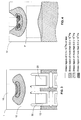
- a thermal conductivity of the IR receiving element 1 of the present invention is analyzed by the use of a finite element method. That is, after a heat amount of 0.1 ⁇ W is provided to the patch 11 , a thermal-diffusion distribution is determined when the substrate reaches a thermally steady state. The result is shown in FIG. 5. It shows that a temperature region of more than 0.4 x 10 -4 °C does not reach the support end 16 . Therefore, it is possible to reduce the substrate length L as long as the temperature region is spaced away from the support end 16 . From results of further simulations, it is obtained that a minimum length of the IR receiving element 1 having four U-shaped slits 30 is 4.5 mm. According to these simulations, it has been experimentally confirmed that the present IR receiving element 1 having the length of 4.5 mm exhibits excellent IR sensitivity while preventing the occurrence of popcorn noise without causing any problem in its thermal property.
- Heat-cycle tests were carried out to compare the occurrence of popcorn noise in the IR receiving element 1 of the present invention with the comparative IR receiving element 1H . Those samples are sealed in a test room, and then a temperature in the test room is changed along a heat-cycle curve shown in FIG. 6. Each of keep times T1 to T4 is 30 min. In the heat-cycle tests, three temperature gradients of 0.5 °C/min, 1 °C/min, and 2 °C/min, are adopted. The occurrence of popcorn noise is checked during the respective heat-cycle test. Results show that the occurrence of popcorn noise in the IR receiving element 1 is reduced irrespective of the temperature gradients, as compared with the comparative IR receiving element 1H .
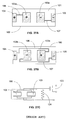
- a pair of positive and negative output terminals 23 and 24 are formed at opposite ends on both of the top and bottom surfaces of the pyroelectric substrate 10 .
- the output terminals 23 and 24 are connected to the first and second electrodes ( 20 , 21 ) by conductive patterns 25 and 26 , as shown in FIGS. 7A and 7B.
- FIG. 7A shows the conductive patterns on the top surface of the substrate 10 .
- FIG. 7B shows the conductive patterns on the bottom surface of the substrate 10 .
- FIG. 7C is a circuit diagram showing a wiring pattern of the IR receiving element 1 with a field-effect transistor FET and a high resistance element R .
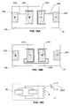
- FIGS. 8A to 8C As first to third modifications of the IR receiving element 1 , it is possible to adopt conductive patterns shown in FIGS. 8A to 8C, FIGS. 9A to 9C, or FIGS. 10A to 10C.
- numeral 27 designate a conductive pattern connecting between the opposed electrodes on the same surface.
- IR receiving elements having various conductive patterns of the present invention can be used to pyroelectric-type IR sensors.
- Desired resist patterns are formed on top and bottom surfaces of a pyroelectric substrate, for example, a single crystal of LiTaO 3 having a thickness of 40 ⁇ m.
- An IR absorbent material is deposited on the substrate surfaces according to the resist patterns to obtain conductive patterns including a first electrode on the top surface and a second electrode on the bottom surface.
- the first and second electrodes are overlapped to each other through the substrate.
- the IR absorbent material is NiCr, it is preferred that a thickness of the respective electrode is determined in a range of about 200 to 500 angstroms.
- a U-shaped slit is formed in the substrate so as to surround continuously three sides of the first and second electrodes by a sandblasting.
- the conductive patterns are protected by the use of a photosensitive dry-film resist during the sandblasting.
- a dry etching process such as ion milling, or wet etching process can be adopted to form the U-shaped slit, however, the sandblasting method is the most preferable to efficiently and accurately form the U-shaped slit in the substrate.
- the IR receiving element is a rectangular shape of 2.5 mm x 5.0 mm, hundreds of the IR receiving elements can be obtained at once from a 3 inch wafer of LiTaO 3 .
- the IR sensor comprises the IR receiving element 1 , a three-dimensional circuit block 2 on which the IR receiving element is mounted, a base plate 3 having three projecting pins 40 to 42 , and a cover 4 having an IR transmittable window 5 on its top surface.
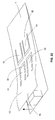
- FIGS. 11 An IR sensor using the present IR receiving element 1 is shown in FIG. 11. That is, the IR sensor comprises the IR receiving element 1 , a three-dimensional circuit block 2 on which the IR receiving element is mounted, a base plate 3 having three projecting pins 40 to 42 , and a cover 4 having an IR transmittable window 5 on its top surface. As shown in FIGS.
- the circuit block 2 is formed with a pair of stands 50 formed on its top surface, a front wall 51 having an IC chip supporting portion 52 , a pair of side walls having a plurality of grooves 53 extending between the front wall 51 and a rear wall 56 , and a pair of stabilizers 54 each having a notch 55 which are formed at a lower side of the front wall 51 .
- the circuit block 2 is integrally molded with an electrically-insulating resin having a low thermal conductivity.
- the IR receiving element 1 is fixed to the stands 50 at the support ends 16 by a conductive bond 9 so as to extend between the stands in a bridge fashion, as shown in FIGS. 13 and 14.
- An IC chip 6 for treating a signal provided from the IR receiving element 1 is attached to the chip supporting portion 52 .
- Electronic components 7 such as condensers, resistors, and field-effect transistors, are mounted on the rear wall 56 .
- the IC chip 6 is electrically connected to the electronic components 7 through conductive patterns 8 formed on the front wall 51 and the grooves 53 in the side walls.
- the projecting pins 40 and 41 are abutted against the inner surfaces of the notches 55 , they are electrically connected to conductive patterns 8 formed on the stabilizers 54 by a conductive bond.
- the circuit block 2 is mechanically connected to the base plate 3 by the conductive bond, as shown in FIG. 11.
- the projecting pin 42 is used to ground.
- numeral 60 designates wires connecting between the IC chip 6 and the conductive patterns 8 formed on the front wall 51 of the circuit block 2 .
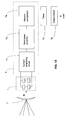
- an operation mechanism of the present IR sensor is briefly explained referring to FIG. 15.
- an output signal is provided from the IR receiving element 1 to a current amplifying circuit 72 .
- a signal having a required frequency is extracted from the amplified signal by a band-pass amplifier 73 .
- the extracted signal is sent to a window comparator 74 in which a threshold value is predetermined.
- a detection signal is output from the comparator 74 .
- an output circuit 76 applies a load to an electric apparatus such as lights for a time period predetermined by a timer 75 .
- numeral 71 designates a condenser of IR rays.
- the current amplifying circuit 72 , band-pass amplifier 73 , and the comparator 74 are incorporated in the IC chip 6, it is possible to use a chip ceramic condenser having a relatively small capacity as well as Al(aluminum)-electrolytic condenser or Ta(tantalum) condenser having a relatively large capacity.
- an IC chip incorporating therein only the current amplifying circuit 72 and band-pass amplifier 73 is mounted on the chip supporting portion 52 , an analog signal can be output from the projecting pins 40 and 41 of the base plate 3 .
- an adequate IC chip may be mounted on the circuit block 2 in accordance with the circumstances.
- FIG. 16 a pyroelectric-type IR receiving element 1A is shown in FIG. 16.
- the IR receiving element 1A is substantially same as that of the above embodiment except that only one pair of patches 11A and 12A are formed in a pyroelectric substrate 10A . Therefore, no duplicate explanation to common parts is deemed necessary.
- Like parts are designated by like numerals with a suffixed letter of " A ".
- conductive patterns formed on top and bottom surfaces of the IR receiving element 1A are shown in FIGS 17A and 17B, respectively.
- FIG. 17C shows a wiring pattern of the IR receiving element 1A with a field-effect transistor FET and high resistance element R .
- a pyroelectric-type IR receiving element 1C is shown in FIG. 19.
- the IR receiving element 1C is substantially same as that of the above embodiment except that patches 11C and 13C are opposed to the patches 12C and 14C through a common base slit 32C , and the patches 11C and 12C are opposed to the patches 13C and 14C through common side slits 31C , respectively. Therefore, no duplicate explanation to common parts is deemed necessary.
- Like parts are designated by like numerals with a suffixed letter of " C ".
- a pyroelectric-type IR receiving element 1D is shown in FIG. 20.
- the IR receiving element 1D is substantially same as that of the above embodiment except that both ends of each of U-shaped slits 30D are bent toward the inside of the U-shaped slit 30D to obtain a neck portion 34 at a cantilever end 15D . Therefore, no duplicate explanation to common parts is deemed necessary.
- Like parts are designated by like numerals with a suffixed letter of " D ".
- a pyroelectric-type IR receiving element 1E is shown in FIG. 21.
- the IR receiving element 1E is substantially same as that of the above embodiment except that both ends of each of U-shaped slits 30E are formed with rounded holes 35 having a diameter larger than its slit width to obtain a neck portion 34E at a cantilever end 15E . Therefore, no duplicate explanation to common parts is deemed necessary.
- Like parts are designated by like numerals with a suffixed letter of " E ".
- a simulation for estimating stress absorbing capability is carried out with respect to the IR receiving elements 1 , 1D and 1E . That is, this simulation is to analyze a stress distribution applied to the respective IR receiving element when one end of the IR receiving element is fixed, and the other end is forcedly lifted up, as shown by an arrow in FIG. 22. Results are shown in FIGS. 23, 24, and 25.
- the result of FIG. 23 shows that no stress region of more than 0.4 x 10 9 Pa is observed on the patches 11 and 13 under the electrodes 20 , however, such a stress region is observed in the vicinity of the cantilever end 15 .
- stress regions of more than 1.6 x 10 9 Pa are observed at the ends of the U-shaped slit 30 .
- the result of FIG. 24 shows that no stress region of more than 0.4 x 10 9 Pa is observed on the patches 11D and 13D under the electrodes 20D , and the development of the stress region at a cantilever end 15D is slightly reduced as compared with that of the IR receiving element 1 . That is, a maximum principal stress applied to the IR receiving element 1D is reduced by as much as 13 %.
- no stress region of more than 1.6 x 10 9 Pa is observed on a pyroelectric substrate 10D of the IR receiving element 1D .
- the IR receiving elements 1D and 1E having unique end shapes of the U-shaped slits 30D and 30 E can provide further improvement of the stress absorbing capability. This means that the occurrence of popcorn noise can be prevented more effectively.
Landscapes
- Physics & Mathematics (AREA)
- General Physics & Mathematics (AREA)
- Spectroscopy & Molecular Physics (AREA)
- Engineering & Computer Science (AREA)
- Power Engineering (AREA)
- Photometry And Measurement Of Optical Pulse Characteristics (AREA)
- Radiation Pyrometers (AREA)
Applications Claiming Priority (6)
| Application Number | Priority Date | Filing Date | Title |
|---|---|---|---|
| JP11840696 | 1996-04-15 | ||
| JP11840696 | 1996-04-15 | ||
| JP118406/96 | 1996-04-15 | ||
| JP10076996A JP3211074B2 (ja) | 1996-04-23 | 1996-04-23 | 赤外線検出器 |
| JP100769/96 | 1996-04-23 | ||
| JP10076996 | 1996-04-23 |
Publications (2)
| Publication Number | Publication Date |
|---|---|
| EP0802402A1 true EP0802402A1 (fr) | 1997-10-22 |
| EP0802402B1 EP0802402B1 (fr) | 2003-06-18 |
Family
ID=26441728
Family Applications (1)
| Application Number | Title | Priority Date | Filing Date |
|---|---|---|---|
| EP97106200A Expired - Lifetime EP0802402B1 (fr) | 1996-04-15 | 1997-04-15 | Elément récepteur pyroélectrique pour l'infrarouge et détecteur d'infrarouge l'utilisant |
Country Status (7)
| Country | Link |
|---|---|
| US (1) | US6121614A (fr) |
| EP (1) | EP0802402B1 (fr) |
| KR (1) | KR100218560B1 (fr) |
| CN (1) | CN1054687C (fr) |
| DE (1) | DE69722846T2 (fr) |
| SG (1) | SG52956A1 (fr) |
| TW (1) | TW346688B (fr) |
Cited By (1)
| Publication number | Priority date | Publication date | Assignee | Title |
|---|---|---|---|---|
| EP1108997A3 (fr) * | 1999-12-17 | 2003-10-08 | Matsushita Electric Works, Ltd. | Elément récepteur de rayons infrarouges et senseur de rayonnement infrarouge utilisant celui-ci |
Families Citing this family (12)
| Publication number | Priority date | Publication date | Assignee | Title |
|---|---|---|---|---|
| JP3289677B2 (ja) * | 1998-05-25 | 2002-06-10 | 株式会社村田製作所 | 赤外線センサ |
| US7157709B2 (en) * | 2002-06-25 | 2007-01-02 | Matsushita Electric Works, Ltd. | Infrared sensor package |
| US7351972B2 (en) * | 2004-08-19 | 2008-04-01 | Drs Sensors & Targeting Systems, Inc. | Infrared radiation image having sub-pixelization and detector interdigitation |
| US7791014B2 (en) * | 2005-03-09 | 2010-09-07 | Asahi Kasei Emd Corporation | Optical device and a method of manufacturing an optical device having a photoelectric conversion element and an optical adjustment element |
| FR2901609B1 (fr) * | 2006-05-24 | 2009-01-16 | Airbus France Sas | Dispositif de controle non destructif d'une piece par analyse de dissipation de rayonnement |
| JP5989296B2 (ja) * | 2010-04-28 | 2016-09-07 | ソニー株式会社 | 赤外線撮像装置 |
| JP5838343B2 (ja) | 2010-06-25 | 2016-01-06 | パナソニックIpマネジメント株式会社 | 焦電型赤外線検知素子およびそれを用いた赤外線センサ |
| CN102377919A (zh) * | 2010-08-17 | 2012-03-14 | 深圳富泰宏精密工业有限公司 | 相机模组及应用该相机模组的便携式电子装置 |
| WO2012114579A1 (fr) | 2011-02-24 | 2012-08-30 | 日本碍子株式会社 | Élément pyroélectrique |
| CN102565059B (zh) * | 2011-12-27 | 2013-11-06 | 郑州炜盛电子科技有限公司 | 复合封装四通道热释电红外传感器 |
| US9207120B2 (en) * | 2013-07-15 | 2015-12-08 | The Boeing Company | Systems and methods for detecting multiple infrared bands |
| TWI646672B (zh) | 2017-12-01 | 2019-01-01 | 財團法人工業技術研究院 | 紅外線感測元件及其製造方法 |
Citations (1)
| Publication number | Priority date | Publication date | Assignee | Title |
|---|---|---|---|---|
| GB2278496A (en) * | 1993-05-24 | 1994-11-30 | Mitsubishi Electric Corp | Infrared detecting element |
Family Cites Families (6)
| Publication number | Priority date | Publication date | Assignee | Title |
|---|---|---|---|---|
| JPH073362B2 (ja) * | 1984-06-14 | 1995-01-18 | 株式会社村田製作所 | 一次元焦電型センサアレイ |
| JPS63138221A (ja) * | 1986-11-28 | 1988-06-10 | Nec Corp | 焦電センサ− |
| GB8812958D0 (en) * | 1988-06-01 | 1988-10-05 | Thorn Emi Electronics Ltd | Thermal imaging |
| US5270555A (en) * | 1989-05-18 | 1993-12-14 | Murata Manufacturing Co., Ltd. | Pyroelectric IR-sensor with a molded inter connection device substrate having a low thermal conductivity coefficient |
| GB2274543A (en) * | 1993-01-21 | 1994-07-27 | Central Research Lab Ltd | Infrared detector |
| JPH07174623A (ja) * | 1993-12-21 | 1995-07-14 | Murata Mfg Co Ltd | 焦電型赤外線センサ及びその製造方法 |
-
1997
- 1997-04-12 TW TW086104715A patent/TW346688B/zh not_active IP Right Cessation
- 1997-04-14 US US08/837,105 patent/US6121614A/en not_active Expired - Lifetime
- 1997-04-14 SG SG1997001204A patent/SG52956A1/en unknown
- 1997-04-15 CN CN97104007A patent/CN1054687C/zh not_active Expired - Lifetime
- 1997-04-15 DE DE69722846T patent/DE69722846T2/de not_active Expired - Lifetime
- 1997-04-15 EP EP97106200A patent/EP0802402B1/fr not_active Expired - Lifetime
- 1997-04-15 KR KR1019970014367A patent/KR100218560B1/ko not_active Expired - Lifetime
Patent Citations (1)
| Publication number | Priority date | Publication date | Assignee | Title |
|---|---|---|---|---|
| GB2278496A (en) * | 1993-05-24 | 1994-11-30 | Mitsubishi Electric Corp | Infrared detecting element |
Non-Patent Citations (1)
| Title |
|---|
| PATENT ABSTRACTS OF JAPAN * |
Cited By (1)
| Publication number | Priority date | Publication date | Assignee | Title |
|---|---|---|---|---|
| EP1108997A3 (fr) * | 1999-12-17 | 2003-10-08 | Matsushita Electric Works, Ltd. | Elément récepteur de rayons infrarouges et senseur de rayonnement infrarouge utilisant celui-ci |
Also Published As
| Publication number | Publication date |
|---|---|
| US6121614A (en) | 2000-09-19 |
| TW346688B (en) | 1998-12-01 |
| KR970070968A (ko) | 1997-11-07 |
| CN1163396A (zh) | 1997-10-29 |
| KR100218560B1 (ko) | 1999-09-01 |
| DE69722846D1 (de) | 2003-07-24 |
| SG52956A1 (en) | 1998-09-28 |
| DE69722846T2 (de) | 2003-12-11 |
| EP0802402B1 (fr) | 2003-06-18 |
| HK1002663A1 (en) | 1998-09-11 |
| CN1054687C (zh) | 2000-07-19 |
Similar Documents
| Publication | Publication Date | Title |
|---|---|---|
| EP0802402B1 (fr) | Elément récepteur pyroélectrique pour l'infrarouge et détecteur d'infrarouge l'utilisant | |
| JP3204130B2 (ja) | 焦電型赤外線センサ素子 | |
| US20020136664A1 (en) | Absolute humidity sensor | |
| JP3281217B2 (ja) | 半導体式加速度センサと該センサのセンサ素子の特性評価方法 | |
| JP3391236B2 (ja) | 赤外線センサ | |
| JPH102793A (ja) | 焦電型赤外線検知素子及び焦電型赤外線センサ | |
| JP3147786B2 (ja) | 加速度センサ | |
| JP3211074B2 (ja) | 赤外線検出器 | |
| US20040112663A1 (en) | Method and device for recognition of a side impact on a motor vehicle | |
| JP3829459B2 (ja) | 焦電型赤外線検知素子 | |
| JP2527881B2 (ja) | チップネットワ―ク抵抗器 | |
| JPH10300571A (ja) | 焦電型赤外線検出装置における電流電圧変換回路 | |
| JPH06160183A (ja) | 赤外線検出器 | |
| KR20040063050A (ko) | 히터 내장형 감습센서 모듈 및 이를 이용한 습도 측정 방법 | |
| JP2576453B2 (ja) | 充電検知器 | |
| JP2734844B2 (ja) | 赤外線検出器 | |
| JP3257879B2 (ja) | ボンディングワイヤの短絡検出装置 | |
| JP2004279118A (ja) | 焦電型赤外線検出器 | |
| JPH07198479A (ja) | 焦電型赤外線センサ | |
| JP3435065B2 (ja) | 圧電式加速度センサ | |
| RU2076315C1 (ru) | Резистивный газовый датчик | |
| JP2002208829A (ja) | 圧電共振素子の不良検出方法 | |
| JPH09126885A (ja) | 焦電型赤外線検出器 | |
| JPH06137942A (ja) | 赤外線検出器 | |
| JPH06160175A (ja) | 赤外線検出素子 |
Legal Events
| Date | Code | Title | Description |
|---|---|---|---|
| PUAI | Public reference made under article 153(3) epc to a published international application that has entered the european phase |
Free format text: ORIGINAL CODE: 0009012 |
|
| AK | Designated contracting states |
Kind code of ref document: A1 Designated state(s): DE GB IT |
|
| RAP1 | Party data changed (applicant data changed or rights of an application transferred) |
Owner name: MATSUSHITA ELECTRIC WORKS, LTD. |
|
| 17P | Request for examination filed |
Effective date: 19971204 |
|
| GRAH | Despatch of communication of intention to grant a patent |
Free format text: ORIGINAL CODE: EPIDOS IGRA |
|
| GRAH | Despatch of communication of intention to grant a patent |
Free format text: ORIGINAL CODE: EPIDOS IGRA |
|
| GRAA | (expected) grant |
Free format text: ORIGINAL CODE: 0009210 |
|
| AK | Designated contracting states |
Designated state(s): DE GB IT |
|
| REG | Reference to a national code |
Ref country code: GB Ref legal event code: FG4D |
|
| REF | Corresponds to: |
Ref document number: 69722846 Country of ref document: DE Date of ref document: 20030724 Kind code of ref document: P |
|
| PLBE | No opposition filed within time limit |
Free format text: ORIGINAL CODE: 0009261 |
|
| STAA | Information on the status of an ep patent application or granted ep patent |
Free format text: STATUS: NO OPPOSITION FILED WITHIN TIME LIMIT |
|
| 26N | No opposition filed |
Effective date: 20040319 |
|
| PGFP | Annual fee paid to national office [announced via postgrant information from national office to epo] |
Ref country code: GB Payment date: 20160413 Year of fee payment: 20 Ref country code: DE Payment date: 20160412 Year of fee payment: 20 |
|
| PGFP | Annual fee paid to national office [announced via postgrant information from national office to epo] |
Ref country code: IT Payment date: 20160418 Year of fee payment: 20 |
|
| REG | Reference to a national code |
Ref country code: DE Ref legal event code: R071 Ref document number: 69722846 Country of ref document: DE |
|
| REG | Reference to a national code |
Ref country code: GB Ref legal event code: PE20 Expiry date: 20170414 |
|
| PG25 | Lapsed in a contracting state [announced via postgrant information from national office to epo] |
Ref country code: GB Free format text: LAPSE BECAUSE OF EXPIRATION OF PROTECTION Effective date: 20170414 |