EP0797088A1 - Mikroplatten mit UVdurchsichtigen Becherböden und Verfahren zu deren Herstellung - Google Patents
Mikroplatten mit UVdurchsichtigen Becherböden und Verfahren zu deren Herstellung Download PDFInfo
- Publication number
- EP0797088A1 EP0797088A1 EP97301686A EP97301686A EP0797088A1 EP 0797088 A1 EP0797088 A1 EP 0797088A1 EP 97301686 A EP97301686 A EP 97301686A EP 97301686 A EP97301686 A EP 97301686A EP 0797088 A1 EP0797088 A1 EP 0797088A1
- Authority
- EP
- European Patent Office
- Prior art keywords
- microplate
- approximately
- wells
- sheet
- layer
- Prior art date
- Legal status (The legal status is an assumption and is not a legal conclusion. Google has not performed a legal analysis and makes no representation as to the accuracy of the status listed.)
- Granted
Links
- 238000000034 method Methods 0.000 title abstract description 32
- 239000000463 material Substances 0.000 claims abstract description 113
- 239000004033 plastic Substances 0.000 claims abstract description 23
- 229920003023 plastic Polymers 0.000 claims abstract description 23
- 230000003287 optical effect Effects 0.000 claims description 31
- 239000002131 composite material Substances 0.000 claims description 8
- -1 polychlorotrifluoroethylene Polymers 0.000 claims description 5
- 239000004831 Hot glue Substances 0.000 claims description 4
- 239000000945 filler Substances 0.000 claims description 4
- DQXBYHZEEUGOBF-UHFFFAOYSA-N but-3-enoic acid;ethene Chemical group C=C.OC(=O)CC=C DQXBYHZEEUGOBF-UHFFFAOYSA-N 0.000 claims description 2
- 239000005038 ethylene vinyl acetate Substances 0.000 claims description 2
- 229920002493 poly(chlorotrifluoroethylene) Polymers 0.000 claims description 2
- 229920001200 poly(ethylene-vinyl acetate) Polymers 0.000 claims description 2
- 239000005023 polychlorotrifluoroethylene (PCTFE) polymer Substances 0.000 claims 1
- 230000005855 radiation Effects 0.000 abstract description 24
- 238000001816 cooling Methods 0.000 abstract description 9
- 238000004519 manufacturing process Methods 0.000 abstract description 9
- 238000002835 absorbance Methods 0.000 abstract description 2
- 239000012768 molten material Substances 0.000 description 35
- 229920004439 Aclar® Polymers 0.000 description 18
- 230000008569 process Effects 0.000 description 15
- 238000003556 assay Methods 0.000 description 13
- 238000000465 moulding Methods 0.000 description 12
- 238000010521 absorption reaction Methods 0.000 description 11
- 230000005540 biological transmission Effects 0.000 description 7
- 229920001577 copolymer Polymers 0.000 description 7
- 238000002347 injection Methods 0.000 description 7
- 239000007924 injection Substances 0.000 description 7
- 239000000523 sample Substances 0.000 description 7
- 239000004793 Polystyrene Substances 0.000 description 6
- 229920002223 polystyrene Polymers 0.000 description 6
- 239000002904 solvent Substances 0.000 description 6
- 239000012963 UV stabilizer Substances 0.000 description 5
- 230000008901 benefit Effects 0.000 description 5
- IAZDPXIOMUYVGZ-UHFFFAOYSA-N Dimethylsulphoxide Chemical compound CS(C)=O IAZDPXIOMUYVGZ-UHFFFAOYSA-N 0.000 description 4
- 230000015572 biosynthetic process Effects 0.000 description 4
- 238000012790 confirmation Methods 0.000 description 4
- 238000000862 absorption spectrum Methods 0.000 description 3
- 238000002474 experimental method Methods 0.000 description 3
- 229920002313 fluoropolymer Polymers 0.000 description 3
- 239000004811 fluoropolymer Substances 0.000 description 3
- 238000002844 melting Methods 0.000 description 3
- 230000008018 melting Effects 0.000 description 3
- 229920000098 polyolefin Polymers 0.000 description 3
- 239000000126 substance Substances 0.000 description 3
- 239000004743 Polypropylene Substances 0.000 description 2
- GWEVSGVZZGPLCZ-UHFFFAOYSA-N Titan oxide Chemical compound O=[Ti]=O GWEVSGVZZGPLCZ-UHFFFAOYSA-N 0.000 description 2
- XLOMVQKBTHCTTD-UHFFFAOYSA-N Zinc monoxide Chemical compound [Zn]=O XLOMVQKBTHCTTD-UHFFFAOYSA-N 0.000 description 2
- 238000004847 absorption spectroscopy Methods 0.000 description 2
- 230000004075 alteration Effects 0.000 description 2
- 235000013405 beer Nutrition 0.000 description 2
- 230000006835 compression Effects 0.000 description 2
- 238000007906 compression Methods 0.000 description 2
- 230000007423 decrease Effects 0.000 description 2
- 230000000694 effects Effects 0.000 description 2
- 229920001519 homopolymer Polymers 0.000 description 2
- 229930195733 hydrocarbon Natural products 0.000 description 2
- 150000002430 hydrocarbons Chemical class 0.000 description 2
- 230000006872 improvement Effects 0.000 description 2
- 238000010348 incorporation Methods 0.000 description 2
- 238000001746 injection moulding Methods 0.000 description 2
- 238000002156 mixing Methods 0.000 description 2
- 238000012986 modification Methods 0.000 description 2
- 230000004048 modification Effects 0.000 description 2
- 239000000049 pigment Substances 0.000 description 2
- 229920000728 polyester Polymers 0.000 description 2
- 238000006116 polymerization reaction Methods 0.000 description 2
- 229920000306 polymethylpentene Polymers 0.000 description 2
- 229920001155 polypropylene Polymers 0.000 description 2
- 239000010453 quartz Substances 0.000 description 2
- VYPSYNLAJGMNEJ-UHFFFAOYSA-N silicon dioxide Inorganic materials O=[Si]=O VYPSYNLAJGMNEJ-UHFFFAOYSA-N 0.000 description 2
- 239000007787 solid Substances 0.000 description 2
- 238000001228 spectrum Methods 0.000 description 2
- 238000002211 ultraviolet spectrum Methods 0.000 description 2
- HJIAMFHSAAEUKR-UHFFFAOYSA-N (2-hydroxyphenyl)-phenylmethanone Chemical class OC1=CC=CC=C1C(=O)C1=CC=CC=C1 HJIAMFHSAAEUKR-UHFFFAOYSA-N 0.000 description 1
- FJKROLUGYXJWQN-UHFFFAOYSA-N 4-hydroxybenzoic acid Chemical class OC(=O)C1=CC=C(O)C=C1 FJKROLUGYXJWQN-UHFFFAOYSA-N 0.000 description 1
- WSSSPWUEQFSQQG-UHFFFAOYSA-N 4-methyl-1-pentene Chemical compound CC(C)CC=C WSSSPWUEQFSQQG-UHFFFAOYSA-N 0.000 description 1
- ZCILGMFPJBRCNO-UHFFFAOYSA-N 4-phenyl-2H-benzotriazol-5-ol Chemical class OC1=CC=C2NN=NC2=C1C1=CC=CC=C1 ZCILGMFPJBRCNO-UHFFFAOYSA-N 0.000 description 1
- 102000004190 Enzymes Human genes 0.000 description 1
- 108090000790 Enzymes Proteins 0.000 description 1
- CBENFWSGALASAD-UHFFFAOYSA-N Ozone Chemical compound [O-][O+]=O CBENFWSGALASAD-UHFFFAOYSA-N 0.000 description 1
- 239000004698 Polyethylene Substances 0.000 description 1
- 229920001328 Polyvinylidene chloride Polymers 0.000 description 1
- 239000005083 Zinc sulfide Substances 0.000 description 1
- NIXOWILDQLNWCW-UHFFFAOYSA-N acrylic acid group Chemical group C(C=C)(=O)O NIXOWILDQLNWCW-UHFFFAOYSA-N 0.000 description 1
- 239000000654 additive Substances 0.000 description 1
- 150000001412 amines Chemical class 0.000 description 1
- 238000004458 analytical method Methods 0.000 description 1
- 150000004945 aromatic hydrocarbons Chemical class 0.000 description 1
- QVGXLLKOCUKJST-UHFFFAOYSA-N atomic oxygen Chemical compound [O] QVGXLLKOCUKJST-UHFFFAOYSA-N 0.000 description 1
- 238000005842 biochemical reaction Methods 0.000 description 1
- 230000000903 blocking effect Effects 0.000 description 1
- 238000003490 calendering Methods 0.000 description 1
- 239000006229 carbon black Substances 0.000 description 1
- 230000015556 catabolic process Effects 0.000 description 1
- 230000008859 change Effects 0.000 description 1
- 238000010276 construction Methods 0.000 description 1
- 238000003851 corona treatment Methods 0.000 description 1
- 230000003247 decreasing effect Effects 0.000 description 1
- 238000006731 degradation reaction Methods 0.000 description 1
- 238000013461 design Methods 0.000 description 1
- 230000001627 detrimental effect Effects 0.000 description 1
- 239000003814 drug Substances 0.000 description 1
- 229940079593 drug Drugs 0.000 description 1
- 239000002359 drug metabolite Substances 0.000 description 1
- 230000005284 excitation Effects 0.000 description 1
- 238000001125 extrusion Methods 0.000 description 1
- 238000001506 fluorescence spectroscopy Methods 0.000 description 1
- 239000007850 fluorescent dye Substances 0.000 description 1
- 238000010438 heat treatment Methods 0.000 description 1
- 239000012943 hotmelt Substances 0.000 description 1
- 229910052500 inorganic mineral Inorganic materials 0.000 description 1
- 239000011159 matrix material Substances 0.000 description 1
- 238000005259 measurement Methods 0.000 description 1
- 239000011707 mineral Substances 0.000 description 1
- 239000000203 mixture Substances 0.000 description 1
- 239000000178 monomer Substances 0.000 description 1
- 150000002816 nickel compounds Chemical class 0.000 description 1
- 102000039446 nucleic acids Human genes 0.000 description 1
- 108020004707 nucleic acids Proteins 0.000 description 1
- 150000007523 nucleic acids Chemical class 0.000 description 1
- 229910052760 oxygen Inorganic materials 0.000 description 1
- 239000001301 oxygen Substances 0.000 description 1
- 230000035699 permeability Effects 0.000 description 1
- 229920002239 polyacrylonitrile Polymers 0.000 description 1
- 239000004417 polycarbonate Substances 0.000 description 1
- 229920000515 polycarbonate Polymers 0.000 description 1
- 229920000573 polyethylene Polymers 0.000 description 1
- 229920000642 polymer Polymers 0.000 description 1
- 239000011116 polymethylpentene Substances 0.000 description 1
- 229920002620 polyvinyl fluoride Polymers 0.000 description 1
- 102000004169 proteins and genes Human genes 0.000 description 1
- 108090000623 proteins and genes Proteins 0.000 description 1
- 230000009467 reduction Effects 0.000 description 1
- 238000009877 rendering Methods 0.000 description 1
- GDESWOTWNNGOMW-UHFFFAOYSA-N resorcinol monobenzoate Chemical class OC1=CC=CC(OC(=O)C=2C=CC=CC=2)=C1 GDESWOTWNNGOMW-UHFFFAOYSA-N 0.000 description 1
- 150000003873 salicylate salts Chemical class 0.000 description 1
- 230000035945 sensitivity Effects 0.000 description 1
- 238000007614 solvation Methods 0.000 description 1
- 230000003595 spectral effect Effects 0.000 description 1
- 239000000454 talc Substances 0.000 description 1
- 229910052623 talc Inorganic materials 0.000 description 1
- 229920001169 thermoplastic Polymers 0.000 description 1
- 239000004416 thermosoftening plastic Substances 0.000 description 1
- 239000004408 titanium dioxide Substances 0.000 description 1
- WBYWAXJHAXSJNI-VOTSOKGWSA-M trans-cinnamate Chemical class [O-]C(=O)\C=C\C1=CC=CC=C1 WBYWAXJHAXSJNI-VOTSOKGWSA-M 0.000 description 1
- 238000000870 ultraviolet spectroscopy Methods 0.000 description 1
- XLYOFNOQVPJJNP-UHFFFAOYSA-N water Substances O XLYOFNOQVPJJNP-UHFFFAOYSA-N 0.000 description 1
- 239000011787 zinc oxide Substances 0.000 description 1
- 229910052984 zinc sulfide Inorganic materials 0.000 description 1
- DRDVZXDWVBGGMH-UHFFFAOYSA-N zinc;sulfide Chemical compound [S-2].[Zn+2] DRDVZXDWVBGGMH-UHFFFAOYSA-N 0.000 description 1
Images


Classifications
-
- B—PERFORMING OPERATIONS; TRANSPORTING
- B01—PHYSICAL OR CHEMICAL PROCESSES OR APPARATUS IN GENERAL
- B01L—CHEMICAL OR PHYSICAL LABORATORY APPARATUS FOR GENERAL USE
- B01L3/00—Containers or dishes for laboratory use, e.g. laboratory glassware; Droppers
- B01L3/50—Containers for the purpose of retaining a material to be analysed, e.g. test tubes
- B01L3/508—Containers for the purpose of retaining a material to be analysed, e.g. test tubes rigid containers not provided for above
- B01L3/5085—Containers for the purpose of retaining a material to be analysed, e.g. test tubes rigid containers not provided for above for multiple samples, e.g. microtitration plates
-
- B—PERFORMING OPERATIONS; TRANSPORTING
- B29—WORKING OF PLASTICS; WORKING OF SUBSTANCES IN A PLASTIC STATE IN GENERAL
- B29C—SHAPING OR JOINING OF PLASTICS; SHAPING OF MATERIAL IN A PLASTIC STATE, NOT OTHERWISE PROVIDED FOR; AFTER-TREATMENT OF THE SHAPED PRODUCTS, e.g. REPAIRING
- B29C45/00—Injection moulding, i.e. forcing the required volume of moulding material through a nozzle into a closed mould; Apparatus therefor
- B29C45/14—Injection moulding, i.e. forcing the required volume of moulding material through a nozzle into a closed mould; Apparatus therefor incorporating preformed parts or layers, e.g. injection moulding around inserts or for coating articles
- B29C45/1418—Injection moulding, i.e. forcing the required volume of moulding material through a nozzle into a closed mould; Apparatus therefor incorporating preformed parts or layers, e.g. injection moulding around inserts or for coating articles the inserts being deformed or preformed, e.g. by the injection pressure
-
- B—PERFORMING OPERATIONS; TRANSPORTING
- B29—WORKING OF PLASTICS; WORKING OF SUBSTANCES IN A PLASTIC STATE IN GENERAL
- B29C—SHAPING OR JOINING OF PLASTICS; SHAPING OF MATERIAL IN A PLASTIC STATE, NOT OTHERWISE PROVIDED FOR; AFTER-TREATMENT OF THE SHAPED PRODUCTS, e.g. REPAIRING
- B29C45/00—Injection moulding, i.e. forcing the required volume of moulding material through a nozzle into a closed mould; Apparatus therefor
- B29C45/14—Injection moulding, i.e. forcing the required volume of moulding material through a nozzle into a closed mould; Apparatus therefor incorporating preformed parts or layers, e.g. injection moulding around inserts or for coating articles
- B29C45/14336—Coating a portion of the article, e.g. the edge of the article
- B29C45/14344—Moulding in or through a hole in the article, e.g. outsert moulding
-
- B—PERFORMING OPERATIONS; TRANSPORTING
- B29—WORKING OF PLASTICS; WORKING OF SUBSTANCES IN A PLASTIC STATE IN GENERAL
- B29C—SHAPING OR JOINING OF PLASTICS; SHAPING OF MATERIAL IN A PLASTIC STATE, NOT OTHERWISE PROVIDED FOR; AFTER-TREATMENT OF THE SHAPED PRODUCTS, e.g. REPAIRING
- B29C45/00—Injection moulding, i.e. forcing the required volume of moulding material through a nozzle into a closed mould; Apparatus therefor
- B29C45/14—Injection moulding, i.e. forcing the required volume of moulding material through a nozzle into a closed mould; Apparatus therefor incorporating preformed parts or layers, e.g. injection moulding around inserts or for coating articles
- B29C45/14778—Injection moulding, i.e. forcing the required volume of moulding material through a nozzle into a closed mould; Apparatus therefor incorporating preformed parts or layers, e.g. injection moulding around inserts or for coating articles the article consisting of a material with particular properties, e.g. porous, brittle
-
- G—PHYSICS
- G01—MEASURING; TESTING
- G01N—INVESTIGATING OR ANALYSING MATERIALS BY DETERMINING THEIR CHEMICAL OR PHYSICAL PROPERTIES
- G01N21/00—Investigating or analysing materials by the use of optical means, i.e. using sub-millimetre waves, infrared, visible or ultraviolet light
- G01N21/01—Arrangements or apparatus for facilitating the optical investigation
- G01N21/03—Cuvette constructions
-
- G—PHYSICS
- G01—MEASURING; TESTING
- G01N—INVESTIGATING OR ANALYSING MATERIALS BY DETERMINING THEIR CHEMICAL OR PHYSICAL PROPERTIES
- G01N21/00—Investigating or analysing materials by the use of optical means, i.e. using sub-millimetre waves, infrared, visible or ultraviolet light
- G01N21/17—Systems in which incident light is modified in accordance with the properties of the material investigated
- G01N21/25—Colour; Spectral properties, i.e. comparison of effect of material on the light at two or more different wavelengths or wavelength bands
- G01N21/31—Investigating relative effect of material at wavelengths characteristic of specific elements or molecules, e.g. atomic absorption spectrometry
- G01N21/33—Investigating relative effect of material at wavelengths characteristic of specific elements or molecules, e.g. atomic absorption spectrometry using ultraviolet light
-
- B—PERFORMING OPERATIONS; TRANSPORTING
- B01—PHYSICAL OR CHEMICAL PROCESSES OR APPARATUS IN GENERAL
- B01L—CHEMICAL OR PHYSICAL LABORATORY APPARATUS FOR GENERAL USE
- B01L2300/00—Additional constructional details
- B01L2300/08—Geometry, shape and general structure
- B01L2300/0809—Geometry, shape and general structure rectangular shaped
- B01L2300/0829—Multi-well plates; Microtitration plates
-
- B—PERFORMING OPERATIONS; TRANSPORTING
- B01—PHYSICAL OR CHEMICAL PROCESSES OR APPARATUS IN GENERAL
- B01L—CHEMICAL OR PHYSICAL LABORATORY APPARATUS FOR GENERAL USE
- B01L2300/00—Additional constructional details
- B01L2300/12—Specific details about materials
Definitions
- the present invention relates generally to microplates for assaying samples, and more specifically to microplates that have UV permeable bottom wells and methods of making such microplates.
- assays include, for example, biochemical reaction kinetics, DNA melting point determinations, DNA spectral shifts, DNA and protein concentration measurements, excitation/emission of fluorescent probes, enzyme activities, enzyme-cofactor assays, homogeneous assays, drug metabolite assays, drug concentration assays, dispensing confirmation, volume confirmation, solvent concentration confirmation and solvation confirmation.
- UV absorption spectroscopy may be used to study these systems.
- UV absorption spectroscopy offers the advantages of relatively high precision and accuracy.
- Microplates typically consist of a plurality of individual wells formed of polymeric materials. Each well includes sidewalls and a bottom so that an aliquot of a sample may be placed within each well. The wells may be arranged in relatively close proximity in a matrix pattern, allowing samples to be studied individually or as a group. Common sizes for microplates include matrices having dimensions of 4x6 (24 wells) or 8x12 (96 wells), although larger microplates are also used that may include matrices of hundreds or even thousands of wells.
- the materials used to construct a microplate are selected based on the samples to be assayed and the analytical techniques to be used.
- the materials of which the microplate is made should be chemically inert to the components of the sample, and the materials should be impervious to radiation or heating conditions to which the microplate is exposed during the course of an experiment.
- a microplate used in assaying samples by UV absorption should have a UV permeable bottom sheet so that a substantial amount UV radiation can pass through each well and interact with the sample without being absorbed by the well bottom.
- microplates having UV permeable bottom sheets there has been limited progress in manufacturing such microplates.
- One problem in designing these microplates relates to the polymeric materials that are typically used for microplate construction.
- these polymeric materials usually have relatively high UV absorption probabilities. Absorption of UV radiation by the polymeric materials results in the chemical and physical degradation of the microplates. Therefore, to prolong the lifetime of these microplates, UV stabilizers specifically designed to absorb UV radiation are often added to the polymeric materials.
- most known microplates have exceptionally high UV absorption probabilities, rendering them useless for experiments in which UV absorption of samples is used.
- U.S. Patent No. 5,487,872 to Hafeman et al. discloses a microplate designed for assaying samples with UV absorption techniques.
- Hafeman discloses a variety of materials from which the bottom surface of the microplate wells may be formed, including TPX® 4-methylpentene-1 polymer as the preferred material (Mitsui Petrochemical Industries, Japan).
- TPX® 4-methylpentene-1 polymer as the preferred material (Mitsui Petrochemical Industries, Japan).
- TPX® 4-methylpentene-1 polymer Mitsubishi Chemical Industries, Japan
- it is believed that microplates using this material for the well bottoms may have limited sensitivity in certain biochemcial experiments.
- UV absorption in a range between approximately 260 nm to approximately 280 nm is studied, but TPX® has a relatively high optical density in this wavelength range.
- Microplates having a quartz bottom plate glued to a molded body have also been produced.
- the cost of these microplates is often more than two orders of magnitude higher than the cost of a microplate formed entirely from polymeric materials, precluding their use for most studies.
- the materials used to bond the quartz bottom plate to the microplate body may leach into samples contained within the wells of the microplate, contaminating the samples and compromising the reliability of the experimental results.
- the strength of the bond between the bottom plate and the body may deteriorate and form leaks between sample wells.
- microplate that is relatively inexpensive, comparatively durable and includes well bottoms having an acceptable optical density across the entire useful range of the UV spectrum.
- a microplate in one illustrative embodiment of the invention, comprises a frame that forms sidewalls of at least one well and a first layer that forms a bottom of the at least one well.
- the first layer is formed from a plastic material having an average optical density no more than approximately 0.09 at a thickness of approximately 7.5 mils between wavelengths of approximately 200 nm and approximately 300 nm.
- a microplate in another illustrative embodiment of the invention, comprises a frame and a sheet.
- the frame includes an upper portion and a lower portion that is contiguous with the upper portion.
- the upper portion of the frame defines sidewalls of at least one well.
- the sheet defines a bottom of the at least one well, and at least a portion of the sheet is disposed between the upper and lower portions of the frame.
- a method for making a microplate having at least first and second wells, each of the first and second wells having sidewalls and a bottom.
- the method comprises steps of: (A) inserting a sheet of a first material into a mold cavity that includes sections shaped to form the sidewalls of the first and second wells so that the sheet is positioned to form the bottoms of the first and second wells, the first material having an average optical density that is no more than approximately 0.09 at a thickness of approximately 7.5 mils between wavelengths of approximately 200 nm and approximately 300 nm; (B) injecting a molten plastic material into the mold cavity; and (C) cooling the plastic material to form the microplate with the plastic material forming the sidewalls of the first and second wells and the sheet of the first material forming the bottom of each of the first and second wells.
- a method for forming a microplate comprises steps of: (A) providing an upper plate defining sidewalls of at least one well, the upper plate having a lower surface; (B) adhering an intermediate layer to the lower surface of the upper plate; and (C) adhering a sheet of the first material to the intermediate layer so that the sheet of the first material forms a bottom of the at least one well.
- a method for making a microplate having at least first and second wells, each of the first and second wells having sidewalls and a bottom.
- the method comprises steps of: (A) inserting a sheet of a material having at least one hole into a mold cavity that includes sections shaped to form the sidewalls of the first and second wells so that the sheet is positioned to form the bottoms of the first and second wells; (B) injecting a molten first plastic material into the mold cavity; and (C) cooling the first plastic material to form the microplate with the first plastic material forming the sidewalls of the first and second wells and the sheet of the first material forming the bottom of each of the first and second wells.
- a microplate in still a further illustrative embodiment of the invention, comprises a frame that forms sidewalls of at least one well and a first layer that forms a bottom of the at least one well.
- the first layer is formed from a chlorotrifluoropolyethylene, such as Aclar® film, and may have an average optical density of no more than approximately 0.09 at a thickness of approximately 7.5 mils, or may have a larger value if copolymer(s) are incorporated therein.
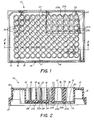
- FIG. 1 An illustrative microplate 10 in accordance with the present invention is shown in Figs. 1 and 2, with Fig. 1 being a partial top and bottom views and Fig. 2 showing a cross-sectional view along line 2-2 of Fig. 1.
- the microplate 10 includes an array of wells 12, each of which may receive an aliquot of a sample to be assayed.
- the microplate includes ninety-six wells arranged in a grid having a plurality of rows and columns.
- the present invention is not limited to this arrangement.
- the present invention can be implemented in any type of microplate arrangement (e.g., all established industry standards such as six, twenty-four, forty-eight, ninety-six, or more wells), and is not limited to any specific number of wells or any specific dimensions.
- Each well includes a top rim 17, sidewalls 16 and a bottom 20. Since the microplate 10 is designed to be used for assaying samples by UV spectroscopy, the bottoms 20 are formed from a UV permeable material. In the embodiment shown in the figures, the bottoms 20 of all the wells are formed from a single sheet 24 of material. The sheet 24 may be rectangular, scalloped along the outer edges as shown in Fig. 3 to conform to the arrangement of the array of wells, or any other shape that is suitable for establishing the bottom 20 of each well.
- UV permeation of a material can be measured in terms of optical density which is defined according to Beer's Law: in which A is the optical density of the material, ⁇ is the wavelength of the radiation incident upon the material, t is the path length of the material through which the radiation passes, P 0 is the power of the radiation incident on the material at the wavelength ⁇ , and P is the power of the radiation that passes the through the material at the wavelength ⁇ at the path length t.
- the optical density of a material depends upon the wavelength of radiation and the path length of the radiation through the material. Therefore, it is convenient to define the UV permeability of a material in terms of the average optical density of the material at a particular thickness and between a specific range of wavelengths.
- references to a UV optical density of a material are intended to indicate the average optical density of the material assuming a thickness of approximately 7.5 mils and a wavelength range between approximately 200 nm and approximately 300 nm. It should be understood that the thickness of approximately 7.5 mils is used solely to provide a common basis for all references to UV optical density, and that no portion of the microplate of the present invention formed from a UV permeable material is limited to that thickness. The thickness of various elements of the microplate of the present invention can vary as described elsewhere herein.
- UV permeable materials suitable for use in the present invention include polymeric materials such as polyolefins, fluoropolymers, polyesters, nonaromatic hydrocarbons, polyvinylidene chlorides and polyhalocarbons, such as polycholortrifluoroethylenes. It is to be understood that, as used herein, a polymeric material may be a homopolymer or a copolymer. Polyolefins may include polyethylenes, polymethylpentenes and polypropylenes, and fluoropolymers may include polyvinyl fluorides.
- UV permeable materials include KynarTM film (3M, Minneapolis, MN), KeIFTM film (3M, Minneapolis, MN) and Aclar® film (Allied Signal, Morristown, NJ). While particular UV permeable materials have been disclosed herein, it should be understood that this list is merely exemplary and not limiting.
- UV stabilizers include, but are not limited to, hydroxybenzophenones, hydroxylphenyl benzotriazoles, hindered amines, organic nickel compounds, salicylates, cinnamate derivatives, resorcinol monobenzoates, oxanilides and p-hydroxybenzoates.
- UV stabilizers increase the optical density of the polymeric materials due to their relatively high UV absorption coefficients. Therefore, according to the present invention, UV permeable materials are preferably substantially free of UV stabilizers.
- Aclar® film is used as the UV permeable material.
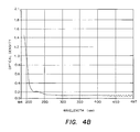
- the UV absorption spectrum of a 7.5 mil sheet of Aclar® film removed from a microplate in accordance with the present invention is shown in Fig. 4A.
- the UV absorption spectrum of a 0.5 mil thick piece of GladTM cling wrap is shown in Fig. 4B
- Fig. 4C depicts the UV absorption spectrum of a 14 mil thick piece of TPX® taken from a Hafeman microplate.
- the spectra shown in Figs. 4A-4C were each taken with an AVIV 14DS spectrophotometer using a 1/3 slit height bandpass of 1.0 nm and a 2 mm by 4 mm aperture.
- the average optical density for the wavelength range between approximately 200 nm and approximately 300 nm for the 0.5 mil GladTM cling wrap piece and the 14 mil TPX® piece are 0.27 and 0.3, respectively.
- the UV optical density of the 7.5 mil sheet of Adar® film is approximately 0.09. While a direct comparison of UV absorption was not made between these materials at a constant thickness, it is known that the optical density of a material decreases as the thickness of the material is increased. Therefore, it is believed that a sheet of Aclar® film having a thickness of 0.5 mil would have a UV optical density of less than 0.27 and that a sheet of Aclar® film having a thickness of 14 mils would have a UV optical density of less than 0.3.
- UV optical density of a 7.5 mil sheet of Aclar® film (approximately 0.09)
- the UV optical density of a sheet of Adar® film, or any other material appropriate for use as sheet 24 may be varied by incorporation of a copolymer or copolymers that are capable of absorbing UV radiation in a wavelength range between approximately 200 nm and approximately 300 nm.
- Chlortrifluoropolyethylene, such as Aclar® film, being a particularly preferred material for inclusion in the microplate is not limited to an average optical density of approximately 0.09 and may have a larger value, such as by the incorporation of copolymer(s), while still being within the invention contemplated herein.
- Aclar® film In addition to having a comparatively low UV optical density, Aclar® film has the property of decreased solvent transmission at temperatures below approximately 250°F-300°F, depending upon the solvent and the thickness of the sheet of Aclar® film.
- a sheet of Aclar® film may have one or both sides corona treated by exposure to ozone formed by an electric discharge in the presence of oxygen.
- corona treatment is not believed to provide any particular advantage for use in the present invention so that a sheet of Aclar® film that has not been corona treated may also be used.
- well bottoms 20 in the microplate of the present invention preferably have a average optical density, measured at wavelengths between approximately 200 nm and approximately 300 nm, of less than approximately 0.09.
- the thicknesses of the well bottoms of the microplate may vary, resulting from a change in crystallinity of portions of sheet 24 due to the diverse temperature range to which sheet 24 may be exposed during the manufacture of microplate 10. Since the variation in well bottom thickness can introduce errors into sample assays, the difference in the average optical density of any two wells, measured at wavelengths between approximately 200 nm and approximately 300 nm, is preferably no greater than approximately 0.09.
- the optical density between wavelengths of approximately 200 nm and approximately 300 nm is not limited to approximately 0.09 and is still within the invention contemplated herein.
- a microplate of the present invention can also used for assays that use visible light (e.g., fluorescence experiments).
- Aclar® film is also believed to be an advantageous material for forming a microplate to be used in this manner because of its solvent resistance.
- sheet 24 To reduce the amount of UV radiation absorbed by well bottoms 20, it is desirable to minimize the thickness of sheet 24. However, if sheet 24 is too thin, solvents and other components of the sample stored in wells 12, such as dimethyl sulfoxide (DMSO), may pass through sheet 24 when microplate 10 is heated during use. It has been found that, to minimize UV absorption while preventing solvent transmission, sheet 24 should have a thickness of less than approximately 14 mils. Preferably, the thickness of sheet 24 is from approximately 2 mils to approximately 9 mils and more preferably from approximately 5 mils to approximately 8 mils. Another advantage of minimizing the thickness of sheet 24 is that, when microplate 10 is constructed according to the molding processes discussed below, stresses between the molded materials and warping of microplate 10 are reduced or eliminated.
- DMSO dimethyl sulfoxide
- microplate 10 includes a frame 14 that supports the wells 12.
- Frame 14 includes outer walls 15 and a top planar surface 13 extending between the outer walls and the wells 12.
- the frame is rectangular in shape.
- Support walls 18 connect the sidewalls 16 of adjacent wells, as shown in Figs. 1-2.
- the wells 12 have circular cross-sections in a plane parallel to the planar surface 13.
- wells 12 may be provided in a number of alternate configurations having different cross-sectional shapes, e.g., rectangles, squares and triangles.
- the outer wall 15 that defines the outer periphery of the frame 14 extends below the bottoms 20 of the wells.
- the outer wall 15 has a bottom edge 21 that extends below the bottom 20 of the wells, so that when placed on a support surface, the microplate is supported by the bottom edges 21 with the well bottoms 20 being raised above the support surface to protect them from damage.
- each outer wall 15 also has a rim 19 to accommodate the skirt of a microplate cover (not shown).
- the microplate of the present invention is constructed so that the material of which the sidewalls 16 are formed is adhered to both the upper and lower surfaces of the sheet 24. In one embodiment, this is achieved by placing holes 28 within the sheet 24 (Fig.
- Aclar® film has a relatively low surface tension even when compared to certain other UV permeable materials. Thus, adhesion of the plastic material to both sides of a sheet of Aclar® film can be particularly advantageous.
- the microplate 10 is provided with a plurality of ribs 22, each of which is formed from the plastic material during the molding processes described below.
- Each of the ribs 22 is contiguous with the sidewalls 16 of an adjacent pair of the plurality of wells 12 and extends below the bottom of its adjacent well bottoms.
- a portion of each rib is formed by molten material that passes through the holes 28 in the sheet 24 during the molding process. This portion of each rib is disposed below and adheres to the lower surface of the sheet 24.
- another portion of each rib is formed by molten material that does not pass through the sheet, but rather, forces the sheet 24 against the section of the mold that defines the rib.
- each rib is disposed above the sheet 24, which is distorted to accommodate this portion of the rib.
- the distorted portions of sheet 24 form a plurality of segments 23 disposed between adjacent well bottoms. A portion of each of the segments 23 is offset from the bottoms of its adjacent wells, such that no plane passing through the bottoms of adjacent wells passes entirely through a segment 23 of the sheet extending therebetween.
- the molten material that forms the ribs and the sidewalls of the microplate can be formed of a material that is impermeable to the type of radiation used in the assay (e.g., UV or visible light).
- the rib grid arrangement is not necessary, and that the microplate 10 can be formed with a different bottom structure that adheres to the lower surface of sheet 24 to securely attach the sheet 24 to the upper portion of the microplate.
- the ribs 22 are oriented in a grid arrangement with some of the ribs 22a extending in rows parallel to the length of the microplate, and others 22b extending in columns perpendicular to the length of the microplate. Segments 23a are disposed along ribs 22a, and segments 23b are disposed along ribs 22b.
- the grid pattern of ribs 22 is shown because this arrangement is simple and economical to manufacture. However, as discussed above, other arrangements may be used.
- frame 14, wells 12, support walls 18 and ribs 22 are made of a UV impermeable material to reduce or eliminate interference from transmission of radiation between adjacent wells.
- a material is considered to be UV impermeable if it has a UV optical density greater than approximately 0.25.
- UV impermeable materials may reflect or absorb UV radiation. Therefore, a UV impermeable material may be formed of a base material that can be UV permeable, that further includes solid pigments that reflect UV radiation (e.g., titanium dioxide, zinc oxide, zinc sulfide and thiopene) or solid pigments that absorb UV radiation (e.g., carbon black). Alternatively, materials which have the inherent property of high UV absorbance may be used.
- UV impermeable materials include, for example, aromatic hydrocarbons and hydrocarbons with extended portions of conjugated unsaturation.
- UV impermeable materials may also be capable of reducing or eliminating the transmission of visible light between adjacent wells which can reduce interference due to transmission of visible light between wells when the microplate is used for assays that use visible light.
- the portions of the microplate other than sheet 24 can be formed from a material impermeable to visible light.
- the sheet 24 and the other portions of microplate 10 can be made of one or more moldable plastics using any of a number of standard fabrication techniques, e.g., injection molding, extrusion, calendering and injection compression.
- plastic material denotes a material comprising a polymerization product incorporating repeating monomer units. Such a polymerization product may be a homopolymer or a copolymer.
- the sheet 24 is formed using a standard fabrication technique, such as any of the ones listed above, into the desired geometrical shape.
- the UV permeable sheet 24 is planar and has the plurality of holes 28 extending therethrough.
- holes 28 may have any shape (e.g., slits, rectangles, squares) so long as they are capable of allowing the molten material to flow therethrough and adhere to the upper and lower surfaces as described below.
- the holes 28 should not be large enough to overlap with well bottoms 20 so that leaking through the holes 28 is avoided.
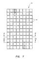
- a two-piece mold can be used having a well-mold piece 38 and a rib-mold piece 40 as shown in Fig. 5.
- Rib-mold piece 40 is placed within a mold piece opening formed by outer mold support piece 55
- well-mold piece 38 is placed within a mold piece opening formed by outer mold support piece 57.
- the sheet 24 that will ultimately form the well bottoms 20 and segments 23 is inserted into the cavity 50 of the rib-mold piece 40 shown in Fig. 6.
- the well-mold piece 38 is then mated with the rib-mold piece 40, enclosing the sheet 24 therebetween.
- the two mold pieces form a chamber 54 that has a shape that conforms to the final shape of the microplate 10.
- Corings or pins 41 prevent the molten material from entering into the area that will form the open areas of wells 12.
- Pins 41 can be an integral part of well-mold piece 38. Alternatively, pins 41 may not be a permanent part of well-mold piece 38 so that, subsequent to fabricating microplate 10, pins 41 may be removed from microplate 10 without removing well-mold piece 38 from microplate 10.
- the rib-mold piece 40 includes channels 56 (Figs. 5-7) that define the regions where the ribs 22 and segments 23 will be formed.
- the portion of the chamber 54 defined by the well-mold piece 38 includes sections that define the shape of the frame 14, well sidewalls 16, support walls 18 and the remaining portions of the microplate that are disposed on the opposite side of the sheet 24 from the ribs 22 and segments 23.
- alternate arrangements of the rib-mold and well-mold pieces can also be employed that would enable the formation of a microplate having the same configuration.
- different arrangements of the rib-mold and well-mold pieces can be used to form microplates having different configurations. For example, since the microplate 10 need not include the ribs 22, a mold piece may be used that does not include the continuous channels 56.
- such a mold piece may have discrete grooves disposed such that, when the sheet 24 is inserted within the mold the holes 28 are disposed above the slots or grooves so that the molten plastic material can flow through the holes 28 and adhere to the lower surface of sheet 24.
- the sheet 24 is positioned in the mold cavity 54 so that one of the holes 28 is disposed at each row/column intersection of channels 56, which correspond to locations where the rows and columns of ribs 22 will intersect and pass entirely through sheet 24.
- the material that will form the upper portion of the microplate and the ribs is then injected in a molten state at high pressure and high temperature into the chamber 54 through an injection gate 48 in the well-mold piece 38.
- the mold cavity 54 does not provide any path for the molten material to pass from the sections of the cavity formed by the well-mold piece 38 into the channels 56, except through the holes 28 or by distorting and forcing the sheet 24 into the channels 56 due to the high pressure of the molten material.
- the molten material upon injection into the chamber 54, partially fills the channels 56 by passing through holes 28, with the other portions of the channels 56 being filled by the sheet 24 being forced into the channels 56 by the molten material from above. It should be understood that it is not necessary for the molten material to distort the sheet 24 or fill the channels 56 to ensure that the sheet 24 is secured. All that is required is that the molten material pass through holes 28 and adhere to the lower surface of the sheet 24.
- knock-outs 43 may be used to apply pressure against microplate 10 to remove it from rib-mold piece 40.
- knock-outs 43 may be located in well-mold piece 38 or in both piece 38 and piece 40.
- a stripper ring may be used to remove microplate 10 from mold piece 38 or mold piece 40.
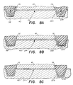
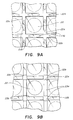
- Figs. 8A-10B demonstrate a process for fabricating a microplate using the mold arrangement shown in Fig. 6 and the molding process described above.
- Figs. 8A-8C depict partial cross-sectional views, taken along line 8-8 of Fig. 7, of the mold arrangement during different stages of the injection molding process and
- Figs. 9A-9B show bottom views of the stages of the molding process depicted in Figs. 8B-8C, respectively.
- Figs. 10A-10B depict partial cross-sectional views of the microplate fabrication process taken along line 10-10 of Fig. 7.
- Figs. 8A and 10A show the initial distortion of film 24 as the molten material is injected through injection gate 48, demonstrating that, as film 24 is distorted, ribs 22a and segments 23a begin to form.
- Fig. 10A demonstrates the flow paths of the molten material, including the molten material that exerts pressure on the film 24 to distort it and the molten material that passes through holes 28 and into channels 56 beneath film 24.
- Fig. 10B shows rib 22a and segments 23a that result.
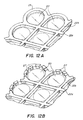
- the mold piece 40 may include additional features 57 or 59 as shown in Figs. 11A-11B disposed within mold piece 40 such that, when the sheet 24 is positioned within rib mold 40, the outer edges of sheet 24 partially overlap the features 57 or 59.
- the portion of the features 57 or 59 that is not located below the outer edges of the sheet 24 allows the molten material to flow around and beneath the outer edge of sheet 24 during the molding process.
- the resulting microplate 10 includes cleats 25 and 27 that adhere to the lower surface of sheet 24 to prevent the outer edges of sheet 24 from peeling away from the sidewalls 16.
- the specific temperature and pressure at which the molten material is injected into the mold varies depending upon the particular material used.
- the pressure of the molten material should be sufficient to allow the molten material to pass through holes 28.
- the temperature should exceed the melting point of the molten material and allow the molten material to flow easily without altering its chemical composition.
- the temperature and pressure should not be so high that the molten material undergoes mixing with the UV permeable sheet, resulting in unusable wells having UV impermeable bottoms, or bottoms with a UV permeable area that is substantially reduced.
- Spectrophotometers and other optical devices have been developed for use with microplates in the standard sizes. To reduce manufacturing costs, it is desirable to use a single mold to produce all microplates at a particular size. Furthermore, it may also be desirable to use a single mold to make microplates from different molten materials. However, different molten materials may shrink by different amounts upon cooling, so the final dimensions of microplates formed from a single mold may vary depending upon the molten material. Because polystyrene is commonly used to construct microplates, molds are often designed considering the mold shrinkage of polystyrene. The term mold shrinkage herein denotes the amount by which a material shrinks upon cooling.
- additives may be incorporated into the molten material to produce a composite material having the mold shrinkage of polystyrene.
- the composite material includes from approximately 30% to 50% filler by weight.
- a composite having approximately the same mold shrinkage as polystyrene can be formed from polypropylene and approximately 40% by weight mineral talc.
- Fig. 13 is a partial cross-sectional view of an alternate embodiment of the present invention in which a microplate 50 is manufactured by adhering an intermediate layer of material 70 to upper plate 60 and subsequently adhering a layer of UV permeable material 80 to the opposite side of intermediate layer 70.
- Upper plate 60 includes wells 12, top rims 17 and sidewalls 16 as describe above.
- upper plate 60 includes a frame 14.
- Upper plate 60 has a smooth surface 62 rather than ribs.
- Upper plate 60 may be molded according to the procedures discussed above. However, a different mold piece is used that is similar to mold piece 40 (Fig. 6) without channels 56 so that upper plate 60 includes smooth surface 62.
- Upper mold 60 and UV permeable layer 80 may be formed of materials that do not readily adhere to each other (e.g., a polyacrylic and Aclar® film). Therefore, to allow upper plate 60 and layer 80 to be incorporated into microplate 50, intermediate layer 70 is provided from a material that adheres to both upper plate 60 and UV permeable material 80.
- Layer 70 may be formed from a hot melt adhesive such as, for example, an ethylene vinyl acetate. In one embodiment, layer 70 is formed from Model 560 Thermo Plastic Bonding Film (3M, Minneapolis, MN).
- Layer 70 may be formed from a UV impermeable material.
- layer 70 should include holes 72 that are arranged so that, subsequent to the manufacture of microplate 50, holes 72 are aligned with the bottoms of wells 12 (Figs. 13 and 14). Although shown in Fig. 14 as being circular in cross-section, holes 72 may have any cross-sectional design so long as layer 70 adheres to both upper plate 50 and layer 80 while not blocking the bottoms of wells 12.
- the layer of UV permeable material 80 has the physical and chemical properties of sheet 24 discussed above. However, unlike sheet 24, material 80 need not include any holes passing therethrough because it need not accept the ribs.
- microplate 50 When layer 70 is formed of a hot melt adhesive, the components of microplate 50 may be adhered using standard conditions and devices for hot melt adhesion. Typically, a pressure of from approximately 40 psig to approximately 80 psig is used at a temperature of from approximately 200°F to approximately 300°F.
- a sheet formed of a corona-treated Aclar® film having a thickness of 7.5 mils and a molecular weight of greater than 10,000 (available from AlliedSignal, Inc., 101 Columbia Road, Morristown, NJ, 07692) was placed within a rib mold piece 40 having channels disposed therein. The rib mold piece was then fitted with a well-mold piece 38. Polystyrene (purchased from BASF, located in Mount Olive, NJ) in a molten state was injected into the cavity through the injection gate 48 at a temperature of approximately 440°F and a pressure of approximately 1200 psig. After filling the cavity with molten material, the pressure was reduced to 500 psig for approximately 6 seconds. The mold was allowed to partially cool by cooling the mold pieces to a temperature between approximately 95°F and 120°F with water. This injection/cooling process was repeated, and the mold was finally cooled and opened to remove the microplate.
- Polystyrene purchased from BASF, located in Mount Olive, NJ
Applications Claiming Priority (2)
| Application Number | Priority Date | Filing Date | Title |
|---|---|---|---|
| US621085 | 1996-03-22 | ||
| US08/621,085 US5858309A (en) | 1996-03-22 | 1996-03-22 | Microplates with UV permeable bottom wells |
Publications (2)
| Publication Number | Publication Date |
|---|---|
| EP0797088A1 true EP0797088A1 (de) | 1997-09-24 |
| EP0797088B1 EP0797088B1 (de) | 2000-05-31 |
Family
ID=24488651
Family Applications (1)
| Application Number | Title | Priority Date | Filing Date |
|---|---|---|---|
| EP97301686A Revoked EP0797088B1 (de) | 1996-03-22 | 1997-03-13 | Mikroplatten mit UVdurchsichtigen Becherböden und Verfahren zu deren Herstellung |
Country Status (4)
| Country | Link |
|---|---|
| US (3) | US5858309A (de) |
| EP (1) | EP0797088B1 (de) |
| JP (1) | JPH1078388A (de) |
| DE (1) | DE69702159T2 (de) |
Cited By (5)
| Publication number | Priority date | Publication date | Assignee | Title |
|---|---|---|---|---|
| WO2000030752A1 (de) * | 1998-11-20 | 2000-06-02 | Molecular Machines & Industries Gmbh | Mehrgefässanordnungen mit verbesserter empfindlichkeit für die optische analytik |
| US6436351B1 (en) | 1998-07-15 | 2002-08-20 | Deltagen Research Laboratories, L.L.C. | Microtitre chemical reaction system |
| EP1524514A1 (de) * | 2002-06-20 | 2005-04-20 | Zeon Corporation | Behälter aus einem polymerharz mit einer alicyclischen struktur und diesen behälter verwendendes optisches messverfahren |
| US8512652B2 (en) | 1997-03-25 | 2013-08-20 | Greiner Bio-One Gmbh | Multiwell microplate with transparent bottom having a thickness less than 200 micrometers |
| US20180200712A1 (en) * | 2015-02-25 | 2018-07-19 | STRATEC CONSUMABLES GmbH | Method of manufacture of microfluidic or microtiter device |
Families Citing this family (67)
| Publication number | Priority date | Publication date | Assignee | Title |
|---|---|---|---|---|
| US6426050B1 (en) * | 1997-05-16 | 2002-07-30 | Aurora Biosciences Corporation | Multi-well platforms, caddies, lids and combinations thereof |
| US6171780B1 (en) | 1997-06-02 | 2001-01-09 | Aurora Biosciences Corporation | Low fluorescence assay platforms and related methods for drug discovery |
| US6229603B1 (en) | 1997-06-02 | 2001-05-08 | Aurora Biosciences Corporation | Low background multi-well plates with greater than 864 wells for spectroscopic measurements |
| US6517781B1 (en) * | 1997-06-02 | 2003-02-11 | Aurora Biosciences Corporation | Low fluorescence assay platforms and related methods for drug discovery |
| US6258326B1 (en) | 1997-09-20 | 2001-07-10 | Ljl Biosystems, Inc. | Sample holders with reference fiducials |
| US6982431B2 (en) * | 1998-08-31 | 2006-01-03 | Molecular Devices Corporation | Sample analysis systems |
| US6297018B1 (en) | 1998-04-17 | 2001-10-02 | Ljl Biosystems, Inc. | Methods and apparatus for detecting nucleic acid polymorphisms |
| US6861035B2 (en) * | 1998-02-24 | 2005-03-01 | Aurora Discovery, Inc. | Multi-well platforms, caddies, lids and combinations thereof |
| US6825042B1 (en) * | 1998-02-24 | 2004-11-30 | Vertex Pharmaceuticals (San Diego) Llc | Microplate lid |
| US6463647B1 (en) * | 1998-03-18 | 2002-10-15 | Corning Incorporated | Method of making an extruded high density assay plate |
| WO1999049973A1 (de) | 1998-03-27 | 1999-10-07 | Aventis Pharma Deutschland Gmbh | Miniaturisierte mikrotiterplatte für hochdurchsatz-screening |
| WO1999055826A1 (en) * | 1998-04-24 | 1999-11-04 | Genova Pharmaceuticals Corporation | Micro-compartmentalization device and uses thereof |
| WO2000072969A1 (en) * | 1999-05-27 | 2000-12-07 | The Perkin-Elmer Corporation | Apparatus and method for the precise location of reaction plates |
| US6399394B1 (en) * | 1999-06-30 | 2002-06-04 | Agilent Technologies, Inc. | Testing multiple fluid samples with multiple biopolymer arrays |
| EP1204856B2 (de) * | 1999-08-20 | 2011-11-16 | Stiftung für Diagnostische Forschung | Verfahren zur bestimmung von substanzen mittels der evaneszenzfeldmethode |
| US7005029B2 (en) * | 1999-10-26 | 2006-02-28 | Nalge Nunc International Corporation | Method of making a multi-well test plate having adhesively secured transparent bottom panel |
| AU1591301A (en) | 1999-11-09 | 2001-06-06 | Sri International | Workstation, apparatus, and methods for the high-throughput synthesis, screeningand characterization of combinatorial libraries |
| US7033840B1 (en) | 1999-11-09 | 2006-04-25 | Sri International | Reaction calorimeter and differential scanning calorimeter for the high-throughput synthesis, screening and characterization of combinatorial libraries |
| EP1315567B1 (de) * | 2000-04-19 | 2010-12-22 | Corning Incorporated | Mehrfachlochplatte und ihr herstellungsverfahren |
| WO2001083109A2 (en) * | 2000-04-28 | 2001-11-08 | Dynex Technologies, Inc. | Low wavelength uv transparent vessels and method for making same |
| US7347977B2 (en) * | 2000-06-08 | 2008-03-25 | Eppendorf Ag | Microtitration plate |
| US20030219816A1 (en) * | 2001-07-02 | 2003-11-27 | Keith Solomon | Composite microarray slides |
| WO2002002585A2 (en) * | 2000-07-05 | 2002-01-10 | Cuno, Inc. | Low fluorescence nylon/glass composites for microdiagnostics |
| US6890483B2 (en) * | 2000-07-05 | 2005-05-10 | Cuno Incorporated | Non-luminescent substrate |
| US7070740B1 (en) * | 2000-09-28 | 2006-07-04 | Beckman Coulter, Inc. | Method and apparatus for processing biomolecule arrays |
| US20020132360A1 (en) * | 2000-11-17 | 2002-09-19 | Flir Systems Boston, Inc. | Apparatus and methods for infrared calorimetric measurements |
| US6821787B2 (en) * | 2000-11-17 | 2004-11-23 | Thermogenic Imaging, Inc. | Apparatus and methods for infrared calorimetric measurements |
| US20040110301A1 (en) * | 2000-11-17 | 2004-06-10 | Neilson Andy C | Apparatus and methods for measuring reaction byproducts |
| GB2369086B (en) * | 2000-11-20 | 2005-06-08 | Herfurth Laser Technology Ltd | Reaction plate |
| US6913732B2 (en) * | 2001-03-19 | 2005-07-05 | Corning Incorporated | Microplate for performing crystallography studies and methods for making and using such microplates |
| PL367715A1 (en) * | 2001-09-20 | 2005-03-07 | 3-Dimensional Pharmaceuticals, Inc. | Conductive microtiter plate |
| US7195872B2 (en) * | 2001-11-09 | 2007-03-27 | 3D Biosurfaces, Inc. | High surface area substrates for microarrays and methods to make same |
| JP4566509B2 (ja) * | 2001-12-28 | 2010-10-20 | 株式会社エンプラス | プラスチックプレート及びプラスチックプレート組立体 |
| US20030183958A1 (en) * | 2002-03-28 | 2003-10-02 | Becton, Dickinson And Company | Multi-well plate fabrication |
| US7537936B2 (en) * | 2002-05-31 | 2009-05-26 | Agilent Technologies, Inc. | Method of testing multiple fluid samples with multiple biopolymer arrays |
| JP2004109107A (ja) * | 2002-07-25 | 2004-04-08 | Nippon Sheet Glass Co Ltd | 生化学用容器 |
| US7128878B2 (en) * | 2002-10-04 | 2006-10-31 | Becton, Dickinson And Company | Multiwell plate |
| US7718442B2 (en) * | 2002-11-22 | 2010-05-18 | Genvault Corporation | Sealed sample storage element system and method |
| JP4229686B2 (ja) * | 2002-11-29 | 2009-02-25 | 日本板硝子株式会社 | 生化学用容器 |
| WO2005033031A1 (ja) * | 2003-10-06 | 2005-04-14 | Nippon Sheet Glass Company, Limited | 紫外線透過ガラス、およびこれを用いたマイクロプレート |
| JP2005134341A (ja) * | 2003-10-31 | 2005-05-26 | Olympus Corp | マイクロプレート |
| US20050173059A1 (en) * | 2004-02-11 | 2005-08-11 | Nalge Nunc International Corporation | Methods of making a multi-well test plate having an adhesively secured transparent bottom panel |
| US20060024209A1 (en) * | 2004-07-30 | 2006-02-02 | Agnew Brian J | Apparatus, methods, and kits for assaying a plurality of fluid samples for a common analyte |
| US7162125B1 (en) * | 2005-06-23 | 2007-01-09 | Sru Biosystems, Inc. | Optimized grating based biosensor and substrate combination |
| JP4473189B2 (ja) * | 2005-07-22 | 2010-06-02 | 株式会社椿本チエイン | 創薬用試料保管システム |
| JP2007240245A (ja) * | 2006-03-07 | 2007-09-20 | Nippon Zeon Co Ltd | 生体分子検査素子用基材及び生体分子検査素子 |
| EP1872854A1 (de) * | 2006-06-30 | 2008-01-02 | PerkinElmer, Inc. | Verbesserte Titerplatte mit mehrfachen Vertiefungen |
| US20080084559A1 (en) * | 2006-10-10 | 2008-04-10 | C Technologies, Inc. | Microvolume sampling device |
| JP2012501681A (ja) | 2008-09-12 | 2012-01-26 | ジェンボールト コーポレイション | 生体分子の貯蔵および安定化のためのマトリックスおよび媒体 |
| JP5767481B2 (ja) * | 2010-02-15 | 2015-08-19 | 丸善石油化学株式会社 | 機能性容器成形方法、成形用金型およびこれらを用いて製造した機能性容器 |
| JP5957850B2 (ja) * | 2011-11-08 | 2016-07-27 | 大日本印刷株式会社 | 細胞培養容器の製造方法 |
| US9790465B2 (en) | 2013-04-30 | 2017-10-17 | Corning Incorporated | Spheroid cell culture well article and methods thereof |
| EP3169451B1 (de) * | 2014-07-17 | 2020-04-01 | University of Washington | Ultraschallsystem zum scheren von zellmaterial |
| TWI512292B (zh) * | 2014-09-04 | 2015-12-11 | Taiwan Green Point Entpr Co | 薄膜式生物晶片之製作方法 |
| SG11201703500XA (en) | 2014-10-29 | 2017-05-30 | Corning Inc | Perfusion bioreactor platform |
| US10809166B2 (en) | 2017-01-20 | 2020-10-20 | Matchstick Technologies, Inc. | Ultrasound system for shearing cellular material in a microplate |
| JP7197557B2 (ja) | 2017-07-14 | 2022-12-27 | コーニング インコーポレイテッド | 多孔性支持体を有する細胞培養槽 |
| US11584906B2 (en) | 2017-07-14 | 2023-02-21 | Corning Incorporated | Cell culture vessel for 3D culture and methods of culturing 3D cells |
| US11857970B2 (en) | 2017-07-14 | 2024-01-02 | Corning Incorporated | Cell culture vessel |
| PL3652290T3 (pl) | 2017-07-14 | 2022-08-22 | Corning Incorporated | Naczynia do hodowli komórkowej 3d do ręcznej lub automatycznej zmiany pożywek |
| US20210023566A1 (en) * | 2018-03-14 | 2021-01-28 | Grainsense Oy | Sample Containers for use Inside Iintegrating Cavities, and Tools |
| US11661574B2 (en) | 2018-07-13 | 2023-05-30 | Corning Incorporated | Fluidic devices including microplates with interconnected wells |
| PL3649229T3 (pl) | 2018-07-13 | 2021-12-06 | Corning Incorporated | Naczynia do hodowli komórkowych ze stabilizującymi urządzeniami |
| CN111032851B (zh) | 2018-07-13 | 2024-03-29 | 康宁股份有限公司 | 具有包含液体介质传递表面的侧壁的微腔皿 |
| USD920536S1 (en) | 2018-09-28 | 2021-05-25 | Becton, Dickinson And Company | Reagent plate |
| US11786903B2 (en) | 2020-03-17 | 2023-10-17 | Covaris, Llc | Multi-component sample holder |
| US20220250063A1 (en) * | 2021-02-10 | 2022-08-11 | Koniku Inc. | Assay system, methods, and multi-well plate for gas stimulation of biological cells, proteins or materials |
Citations (6)
| Publication number | Priority date | Publication date | Assignee | Title |
|---|---|---|---|---|
| EP0106662A2 (de) * | 1982-10-12 | 1984-04-25 | Dynatech Laboratories, Incorporated | Nichtfluoreszierende Behälter zum Halten von Proben in einem Fluoreszenztest |
| EP0170760A1 (de) * | 1983-07-06 | 1986-02-12 | Statens Bakteriologiska Laboratorium | Serologische Diagnose von Streptokokkeninfektion unter Verwendung einer automatischen Ablesung von Mikrotitrationsplatte mit einem Photometer |
| US4892409A (en) * | 1988-07-14 | 1990-01-09 | Smith Harry F | Photometric apparatus for multiwell plates having a positionable lens assembly |
| US5047215A (en) * | 1985-06-18 | 1991-09-10 | Polyfiltronics, Inc. | Multiwell test plate |
| EP0571661A1 (de) * | 1992-05-28 | 1993-12-01 | Packard Instrument Company, Inc. | Mehrbehälter-Versuchsplatte mit Verwendung in Lichtmessung |
| US5487872A (en) * | 1994-04-15 | 1996-01-30 | Molecular Device Corporation | Ultraviolet radiation transparent multi-assay plates |
Family Cites Families (9)
| Publication number | Priority date | Publication date | Assignee | Title |
|---|---|---|---|---|
| IL51668A (en) * | 1977-03-16 | 1981-12-31 | Israel State | Analytical method for the quantitative determination of immunogens and antibodies and a kit therefor |
| US4385115A (en) * | 1980-10-22 | 1983-05-24 | Hoffmann-La Roche Inc. | Diagnostics testing devices and processes |
| US4424067A (en) * | 1982-07-29 | 1984-01-03 | Allied Corporation | Purification of anhydrous hydrogen fluoride |
| EP0148482B1 (de) * | 1983-12-26 | 1992-03-25 | Daikin Industries, Limited | Verfahren zur Herstellung von Halogen enthaltenden Polyäthern |
| US4948442A (en) * | 1985-06-18 | 1990-08-14 | Polyfiltronics, Inc. | Method of making a multiwell test plate |
| EP0627991A1 (de) * | 1992-02-25 | 1994-12-14 | The Dow Chemical Company | Ultraviolettstrahlenreflexionspolymerfilm |
| JPH06349544A (ja) | 1993-06-14 | 1994-12-22 | Sumitomo Wiring Syst Ltd | 車両用充電コネクタ構造 |
| US5487573A (en) | 1993-11-19 | 1996-01-30 | Itt Corporation | Unitary assembly of tubing and a pressed on, interference fit, terminating fitting |
| US5580528A (en) * | 1994-01-14 | 1996-12-03 | Demers; James P. | Breakage resistant laboratory glassware article |
-
1996
- 1996-03-22 US US08/621,085 patent/US5858309A/en not_active Ceased
-
1997
- 1997-03-13 EP EP97301686A patent/EP0797088B1/de not_active Revoked
- 1997-03-13 DE DE69702159T patent/DE69702159T2/de not_active Revoked
- 1997-03-24 JP JP9069791A patent/JPH1078388A/ja active Pending
-
1998
- 1998-09-15 US US09/153,134 patent/US6103169A/en not_active Expired - Lifetime
-
2001
- 2001-01-12 US US09/760,250 patent/USRE38214E1/en not_active Expired - Lifetime
Patent Citations (6)
| Publication number | Priority date | Publication date | Assignee | Title |
|---|---|---|---|---|
| EP0106662A2 (de) * | 1982-10-12 | 1984-04-25 | Dynatech Laboratories, Incorporated | Nichtfluoreszierende Behälter zum Halten von Proben in einem Fluoreszenztest |
| EP0170760A1 (de) * | 1983-07-06 | 1986-02-12 | Statens Bakteriologiska Laboratorium | Serologische Diagnose von Streptokokkeninfektion unter Verwendung einer automatischen Ablesung von Mikrotitrationsplatte mit einem Photometer |
| US5047215A (en) * | 1985-06-18 | 1991-09-10 | Polyfiltronics, Inc. | Multiwell test plate |
| US4892409A (en) * | 1988-07-14 | 1990-01-09 | Smith Harry F | Photometric apparatus for multiwell plates having a positionable lens assembly |
| EP0571661A1 (de) * | 1992-05-28 | 1993-12-01 | Packard Instrument Company, Inc. | Mehrbehälter-Versuchsplatte mit Verwendung in Lichtmessung |
| US5487872A (en) * | 1994-04-15 | 1996-01-30 | Molecular Device Corporation | Ultraviolet radiation transparent multi-assay plates |
Cited By (9)
| Publication number | Priority date | Publication date | Assignee | Title |
|---|---|---|---|---|
| US8512652B2 (en) | 1997-03-25 | 2013-08-20 | Greiner Bio-One Gmbh | Multiwell microplate with transparent bottom having a thickness less than 200 micrometers |
| US6436351B1 (en) | 1998-07-15 | 2002-08-20 | Deltagen Research Laboratories, L.L.C. | Microtitre chemical reaction system |
| WO2000030752A1 (de) * | 1998-11-20 | 2000-06-02 | Molecular Machines & Industries Gmbh | Mehrgefässanordnungen mit verbesserter empfindlichkeit für die optische analytik |
| DE19853640A1 (de) * | 1998-11-20 | 2000-06-08 | Molecular Machines & Ind Gmbh | Mehrgefäßanordnung mit verbesserter Empfindlichkeit für die optische Analytik |
| DE19853640C2 (de) * | 1998-11-20 | 2002-01-31 | Molecular Machines & Ind Gmbh | Mehrgefäßanordnung mit verbesserter Empfindlichkeit für die optische Analytik, Verfahren zu ihrer Herstellung sowie ihre Verwendung in optischen Analyseverfahren |
| EP1524514A1 (de) * | 2002-06-20 | 2005-04-20 | Zeon Corporation | Behälter aus einem polymerharz mit einer alicyclischen struktur und diesen behälter verwendendes optisches messverfahren |
| EP1524514A4 (de) * | 2002-06-20 | 2005-10-12 | Zeon Corp | Behälter aus einem polymerharz mit einer alicyclischen struktur und diesen behälter verwendendes optisches messverfahren |
| US20180200712A1 (en) * | 2015-02-25 | 2018-07-19 | STRATEC CONSUMABLES GmbH | Method of manufacture of microfluidic or microtiter device |
| US20210077997A1 (en) * | 2015-02-25 | 2021-03-18 | STRATEC CONSUMABLES GmbH | Method of Manufacture of Microfluidic or Microtiter Device |
Also Published As
| Publication number | Publication date |
|---|---|
| US5858309A (en) | 1999-01-12 |
| JPH1078388A (ja) | 1998-03-24 |
| EP0797088B1 (de) | 2000-05-31 |
| DE69702159D1 (de) | 2000-07-06 |
| DE69702159T2 (de) | 2000-11-16 |
| US6103169A (en) | 2000-08-15 |
| USRE38214E1 (en) | 2003-08-12 |
Similar Documents
| Publication | Publication Date | Title |
|---|---|---|
| USRE38214E1 (en) | Microplates with UV permeable bottom wells | |
| EP0853496B1 (de) | Mikroplatten zur verhinderung von optischer interferenz zwischen küvetten | |
| US6514464B1 (en) | Micro plate with transparent base | |
| WO1997012678A9 (en) | Microplates which prevent optical cross-talk between wells | |
| US7531140B2 (en) | Multiwell plate having transparent well bottoms and method for making the mulitiwell plate | |
| US20030064508A1 (en) | Conductive microtiter plate | |
| US5487872A (en) | Ultraviolet radiation transparent multi-assay plates | |
| EP0844025B1 (de) | Mikrotestplatten | |
| US20040216835A1 (en) | Method for making a multiwell plate having transparent well bottoms | |
| JP2008249707A (ja) | 分析に用いるデバイスおよび方法 | |
| US20070031296A1 (en) | Improved two-part microwell plates and methods of fabricating same | |
| CA2734816C (en) | Reaction vessel for crystallization of a sample from a solution | |
| US20110064630A1 (en) | Multi-well improved plate | |
| AU2007265789B2 (en) | Improved multi-well assay plate | |
| US20160144359A1 (en) | Reinforced microplate | |
| KR20240025341A (ko) | 씰링 커버와의 부착력이 향상된 다중-웰 플레이트 | |
| AU2002330047A1 (en) | Conductive microtiter plate |
Legal Events
| Date | Code | Title | Description |
|---|---|---|---|
| PUAI | Public reference made under article 153(3) epc to a published international application that has entered the european phase |
Free format text: ORIGINAL CODE: 0009012 |
|
| AK | Designated contracting states |
Kind code of ref document: A1 Designated state(s): DE FR GB IT |
|
| 17P | Request for examination filed |
Effective date: 19980115 |
|
| 17Q | First examination report despatched |
Effective date: 19980302 |
|
| GRAG | Despatch of communication of intention to grant |
Free format text: ORIGINAL CODE: EPIDOS AGRA |
|
| GRAG | Despatch of communication of intention to grant |
Free format text: ORIGINAL CODE: EPIDOS AGRA |
|
| GRAH | Despatch of communication of intention to grant a patent |
Free format text: ORIGINAL CODE: EPIDOS IGRA |
|
| GRAH | Despatch of communication of intention to grant a patent |
Free format text: ORIGINAL CODE: EPIDOS IGRA |
|
| GRAA | (expected) grant |
Free format text: ORIGINAL CODE: 0009210 |
|
| AK | Designated contracting states |
Kind code of ref document: B1 Designated state(s): DE FR GB IT |
|
| REF | Corresponds to: |
Ref document number: 69702159 Country of ref document: DE Date of ref document: 20000706 |
|
| ET | Fr: translation filed | ||
| ITF | It: translation for a ep patent filed |
Owner name: STUDIO TORTA S.R.L. |
|
| PLBQ | Unpublished change to opponent data |
Free format text: ORIGINAL CODE: EPIDOS OPPO |
|
| PLBI | Opposition filed |
Free format text: ORIGINAL CODE: 0009260 |
|
| 26 | Opposition filed |
Opponent name: GREINER BIO-ONE GMBH Effective date: 20010228 |
|
| PLBQ | Unpublished change to opponent data |
Free format text: ORIGINAL CODE: EPIDOS OPPO |
|
| PLAB | Opposition data, opponent's data or that of the opponent's representative modified |
Free format text: ORIGINAL CODE: 0009299OPPO |
|
| PLBI | Opposition filed |
Free format text: ORIGINAL CODE: 0009260 |
|
| REG | Reference to a national code |
Ref country code: GB Ref legal event code: IF02 |
|
| 26 | Opposition filed |
Opponent name: GREINER BIO-ONE GMBH Effective date: 20010228 Opponent name: GREINER BIO-ONE GMBH Effective date: 20010224 |
|
| PLBF | Reply of patent proprietor to notice(s) of opposition |
Free format text: ORIGINAL CODE: EPIDOS OBSO |
|
| PLBJ | Opposition found inadmissible |
Free format text: ORIGINAL CODE: 0009275 |
|
| 26U | Opposition found inadmissible |
Opponent name: GREINER BIO-ONE GMBH Effective date: 20010228 |
|
| PLBF | Reply of patent proprietor to notice(s) of opposition |
Free format text: ORIGINAL CODE: EPIDOS OBSO |
|
| PLBF | Reply of patent proprietor to notice(s) of opposition |
Free format text: ORIGINAL CODE: EPIDOS OBSO |
|
| PLAY | Examination report in opposition despatched + time limit |
Free format text: ORIGINAL CODE: EPIDOSNORE2 |
|
| PLAY | Examination report in opposition despatched + time limit |
Free format text: ORIGINAL CODE: EPIDOSNORE2 |
|
| PLBC | Reply to examination report in opposition received |
Free format text: ORIGINAL CODE: EPIDOSNORE3 |
|
| RDAF | Communication despatched that patent is revoked |
Free format text: ORIGINAL CODE: EPIDOSNREV1 |
|
| APAH | Appeal reference modified |
Free format text: ORIGINAL CODE: EPIDOSCREFNO |
|
| APBP | Date of receipt of notice of appeal recorded |
Free format text: ORIGINAL CODE: EPIDOSNNOA2O |
|
| APBQ | Date of receipt of statement of grounds of appeal recorded |
Free format text: ORIGINAL CODE: EPIDOSNNOA3O |
|
| PGFP | Annual fee paid to national office [announced via postgrant information from national office to epo] |
Ref country code: GB Payment date: 20070327 Year of fee payment: 11 |
|
| PGFP | Annual fee paid to national office [announced via postgrant information from national office to epo] |
Ref country code: DE Payment date: 20070430 Year of fee payment: 11 |
|
| APBU | Appeal procedure closed |
Free format text: ORIGINAL CODE: EPIDOSNNOA9O |
|
| PGFP | Annual fee paid to national office [announced via postgrant information from national office to epo] |
Ref country code: IT Payment date: 20070521 Year of fee payment: 11 |
|
| RDAG | Patent revoked |
Free format text: ORIGINAL CODE: 0009271 |
|
| STAA | Information on the status of an ep patent application or granted ep patent |
Free format text: STATUS: PATENT REVOKED |
|
| 27W | Patent revoked |
Effective date: 20071115 |
|
| GBPR | Gb: patent revoked under art. 102 of the ep convention designating the uk as contracting state |
Free format text: 20071115 |
|
| PGFP | Annual fee paid to national office [announced via postgrant information from national office to epo] |
Ref country code: FR Payment date: 20070319 Year of fee payment: 11 |