EP0795235B1 - N-bit umsetzer mit n-1-grössenverstärkern und n-vergleichern - Google Patents
N-bit umsetzer mit n-1-grössenverstärkern und n-vergleichern Download PDFInfo
- Publication number
- EP0795235B1 EP0795235B1 EP95940069A EP95940069A EP0795235B1 EP 0795235 B1 EP0795235 B1 EP 0795235B1 EP 95940069 A EP95940069 A EP 95940069A EP 95940069 A EP95940069 A EP 95940069A EP 0795235 B1 EP0795235 B1 EP 0795235B1
- Authority
- EP
- European Patent Office
- Prior art keywords
- line
- node
- transistor
- connects
- output
- Prior art date
- Legal status (The legal status is an assumption and is not a legal conclusion. Google has not performed a legal analysis and makes no representation as to the accuracy of the status listed.)
- Expired - Lifetime
Links
- 238000006243 chemical reaction Methods 0.000 abstract description 9
- 230000000694 effects Effects 0.000 abstract description 8
- 238000000034 method Methods 0.000 abstract description 7
- 230000003071 parasitic effect Effects 0.000 description 4
- 238000010276 construction Methods 0.000 description 3
- 230000014509 gene expression Effects 0.000 description 3
- 230000003321 amplification Effects 0.000 description 1
- 230000007423 decrease Effects 0.000 description 1
- 238000010586 diagram Methods 0.000 description 1
- 238000005516 engineering process Methods 0.000 description 1
- 230000010354 integration Effects 0.000 description 1
- 238000012423 maintenance Methods 0.000 description 1
- 238000012986 modification Methods 0.000 description 1
- 230000004048 modification Effects 0.000 description 1
- 238000003199 nucleic acid amplification method Methods 0.000 description 1
- 229910052710 silicon Inorganic materials 0.000 description 1
- 239000010703 silicon Substances 0.000 description 1
Images


Classifications
-
- H—ELECTRICITY
- H03—ELECTRONIC CIRCUITRY
- H03F—AMPLIFIERS
- H03F3/00—Amplifiers with only discharge tubes or only semiconductor devices as amplifying elements
- H03F3/26—Push-pull amplifiers; Phase-splitters therefor
-
- H—ELECTRICITY
- H03—ELECTRONIC CIRCUITRY
- H03F—AMPLIFIERS
- H03F3/00—Amplifiers with only discharge tubes or only semiconductor devices as amplifying elements
- H03F3/45—Differential amplifiers
- H03F3/45071—Differential amplifiers with semiconductor devices only
- H03F3/45076—Differential amplifiers with semiconductor devices only characterised by the way of implementation of the active amplifying circuit in the differential amplifier
- H03F3/4508—Differential amplifiers with semiconductor devices only characterised by the way of implementation of the active amplifying circuit in the differential amplifier using bipolar transistors as the active amplifying circuit
- H03F3/45098—PI types
- H03F3/45103—Non-folded cascode stages
-
- H—ELECTRICITY
- H03—ELECTRONIC CIRCUITRY
- H03F—AMPLIFIERS
- H03F3/00—Amplifiers with only discharge tubes or only semiconductor devices as amplifying elements
- H03F3/45—Differential amplifiers
- H03F3/45071—Differential amplifiers with semiconductor devices only
- H03F3/45076—Differential amplifiers with semiconductor devices only characterised by the way of implementation of the active amplifying circuit in the differential amplifier
- H03F3/4508—Differential amplifiers with semiconductor devices only characterised by the way of implementation of the active amplifying circuit in the differential amplifier using bipolar transistors as the active amplifying circuit
- H03F3/45098—PI types
- H03F3/45107—Folded cascode stages
-
- H—ELECTRICITY
- H03—ELECTRONIC CIRCUITRY
- H03M—CODING; DECODING; CODE CONVERSION IN GENERAL
- H03M1/00—Analogue/digital conversion; Digital/analogue conversion
- H03M1/12—Analogue/digital converters
- H03M1/34—Analogue value compared with reference values
- H03M1/38—Analogue value compared with reference values sequentially only, e.g. successive approximation type
- H03M1/44—Sequential comparisons in series-connected stages with change in value of analogue signal
- H03M1/445—Sequential comparisons in series-connected stages with change in value of analogue signal the stages being of the folding type
-
- H—ELECTRICITY
- H03—ELECTRONIC CIRCUITRY
- H03F—AMPLIFIERS
- H03F2203/00—Indexing scheme relating to amplifiers with only discharge tubes or only semiconductor devices as amplifying elements covered by H03F3/00
- H03F2203/45—Indexing scheme relating to differential amplifiers
- H03F2203/45302—Indexing scheme relating to differential amplifiers the common gate stage of a cascode dif amp being controlled
-
- H—ELECTRICITY
- H03—ELECTRONIC CIRCUITRY
- H03F—AMPLIFIERS
- H03F2203/00—Indexing scheme relating to amplifiers with only discharge tubes or only semiconductor devices as amplifying elements covered by H03F3/00
- H03F2203/45—Indexing scheme relating to differential amplifiers
- H03F2203/45311—Indexing scheme relating to differential amplifiers the common gate stage of a cascode dif amp being implemented by multiple transistors
-
- H—ELECTRICITY
- H03—ELECTRONIC CIRCUITRY
- H03F—AMPLIFIERS
- H03F2203/00—Indexing scheme relating to amplifiers with only discharge tubes or only semiconductor devices as amplifying elements covered by H03F3/00
- H03F2203/45—Indexing scheme relating to differential amplifiers
- H03F2203/45318—Indexing scheme relating to differential amplifiers the AAC comprising a cross coupling circuit, e.g. two extra transistors cross coupled
-
- H—ELECTRICITY
- H03—ELECTRONIC CIRCUITRY
- H03F—AMPLIFIERS
- H03F2203/00—Indexing scheme relating to amplifiers with only discharge tubes or only semiconductor devices as amplifying elements covered by H03F3/00
- H03F2203/45—Indexing scheme relating to differential amplifiers
- H03F2203/45352—Indexing scheme relating to differential amplifiers the AAC comprising a combination of a plurality of transistors, e.g. Darlington coupled transistors
-
- H—ELECTRICITY
- H03—ELECTRONIC CIRCUITRY
- H03F—AMPLIFIERS
- H03F2203/00—Indexing scheme relating to amplifiers with only discharge tubes or only semiconductor devices as amplifying elements covered by H03F3/00
- H03F2203/45—Indexing scheme relating to differential amplifiers
- H03F2203/45371—Indexing scheme relating to differential amplifiers the AAC comprising parallel coupled multiple transistors at their source and gate and drain or at their base and emitter and collector, e.g. in a cascode dif amp, only those forming the composite common source transistor or the composite common emitter transistor respectively
-
- H—ELECTRICITY
- H03—ELECTRONIC CIRCUITRY
- H03F—AMPLIFIERS
- H03F2203/00—Indexing scheme relating to amplifiers with only discharge tubes or only semiconductor devices as amplifying elements covered by H03F3/00
- H03F2203/45—Indexing scheme relating to differential amplifiers
- H03F2203/45702—Indexing scheme relating to differential amplifiers the LC comprising two resistors
-
- H—ELECTRICITY
- H03—ELECTRONIC CIRCUITRY
- H03F—AMPLIFIERS
- H03F2203/00—Indexing scheme relating to amplifiers with only discharge tubes or only semiconductor devices as amplifying elements covered by H03F3/00
- H03F2203/45—Indexing scheme relating to differential amplifiers
- H03F2203/45722—Indexing scheme relating to differential amplifiers the LC comprising one or more source followers, as post buffer or driver stages, in cascade in the LC
Definitions
- the present invention relates to analog-to-digital converters. More specifically, the present invention relates to high speed, low voltage serial-type analog-to-digital converters. An example of such a known converter is disclosed in US Patent No. 4599602.
- A/D converters There are a variety of analog-to-digital (“A/D”) converters. For example, there are parallel encoder (or flash ) A/D converters, multistage A/D conveners, successive approximation A/D converters, voltage -to-frequency A/D converters, dual-ramp A/D converters, and staircase A/D converters. There is such a variety because the need for converters has heightened with the advent of single-chip large scale integration (“LSI”) microprocessors. In fact, in some cases, it is desirable to include such converters on the same chip with the microprocessor.
- LSI large scale integration
- Serial-type A/D converters typically convert analog signals first into Gray scale code and then into binary code. They are configured to have a series of cascaded analog cells to which the Gray scale code-to-binary processing system connects. Each cell of the series of cascaded analog cells has a folding cell which will process the differential input signals, V IL and V IH , according to Figure 1.
- the signals input to the differential input of the folding cell are shown in Figure 1A.
- V IH increases and V IL decreases, there is a single crossing at 100. This crossing point is the input level where the comparator of the folding cell is tripped and the V IH and V IL signals are folded to form the intermediate signals V 1 and V 2 that are shown in Figure1B. These intermediate signals are output from the current switching portion of the folding cell.
- V 1 and V 2 are folded as shown in Figure 1B, the folded signals converge but do not cross as shown at 102.
- V OH and V OL outputs for input to the next stage, it is necessary to further process the V 1 and V 2 signals.
- the processing that is necessary is to offset the V 1 and V 2 signals to align them. Once the offset has been applied, the alignment shown in Figure 1C results. This alignment has crossing points at 104 and at 106. Thereafter, the V OH and V OL signals are input to the next stage of the serial-type A/D converter.
- the signals output from the comparator of the folding cell are input to the Gray scale code-to-binary section of the serial-type A/D converter which result in the binary signals that are used in the digital portions of a much larger circuit.
- the construction of the A/D converter is quite important. Problems that may arise in the analog cells include the maintenance of linearity of the outputs, desensitizing early voltage effects, proper offset of the V 1 and V 2 signals, complexity of the implementation of the circuit in silicon, the production of unwanted and uncompensated parasitics, the need to attain proper device matching within each stage of the serial-type A/D converter, etc.
- the present invention overcomes these problems and provides a serial-type A/D converter that has increased linearity, insensitivity to early voltage effects at the cross-over points, and is not limited to a specific gain.
- the serial-type A/D converter of the present invention will be described in detail in the remainder of the specification referring to the drawings.
- the present invention provides a serial-type A/D n-bit converter, comprising n-1 amplifiers, n comparators, and a Gray scale code-to-binary block, the n-1 amplifiers being cascaded such that an output of one amplifier provides an input to a next amplifier, the outputs of the comparators providing a differential input to the Gray scale block, each of the amplifiers comprising a differential input circuit, for receiving and amplifying the differential analog input (V IH , V IL ), a current switching circuit, coupled to the differential input circuit, for folding the differential analog input, a comparator, receiving the differential analog input (V IH , V IL ) and generating first and second control signals, for controlling the current switching circuit, and first and second outputs, for providing first and second output signals, characterized in that third and fourth output signals, from the current switching circuit are provided to base contacts of buffer transistors, each having one side coupled to an output terminal for providing a folded signal to a next amplifier.
- a converter according to the present invention preferably further comprises a resistor between one of the buffer transistors and the output terminal for aligning the folded signals to create desired crossing points between the folded signals.
- the current switching circuit comprises first, second, third, and fourth switching transistors, the first and second switching transistors forming a first portion of the current switching circuit and the third and fourth switching transistors forming a second portion of the current switching circuit.
- each amplifier includes an amplifier unit and a reference unit, the reference unit having inputs for setting a full scale input range and reference output which match a full scale range of the folded output signals.
- each reference unit includes a second differential input circuit for receiving and amplifying a differential reference signal and for providing an offset current to the amplifying unit to align the first and second folded signals such that a magnitude of one of the first and second folded signals is altered relative to the other.
- a converter according to the present invention may further comprise an inverted cascode-coupled transistor connected between the buffer transistor and the current switching circuit.
- the cascode-coupled transistor has one side coupled to the current switching circuit, and another side coupled to the control lead of an output transistor and also to a load resistor.
- a converter according to the present invention may further comprise the reference unit including a second differential input circuit for receiving a respective differential reference signal, for providing an offset signal to align the first and second output signals, and for providing to the next stage a differential reference output signal.
- each reference unit has first and second differential transistor pairs, the first pair for providing the differential reference output signal, and the second pair for providing the offset signal. More preferably, each reference unit has a third pair of transistors, each transistor in the second pair of transistors being connected on a first side to a respective one of the third pair of transistors and on a second side to a current source, the third pair of transistors being coupled to the first and second output circuits.
- a converter according to the present invention may further comprise the reference circuit coupled to control terminals of the first and second buffer transistors for providing bias voltages thereto.
- a converter according to the present invention may further comprise an amplifying portion with load resistors between the current switching circuit and a voltage source, the converter further including offset circuitry with load resistors coupled to the output terminals, the load resistors in the offset circuitry having half the resistance of the load resistors in the amplifier portion.
- a serial-type A/D converter in a preferred embodiment of the present invention uses magnitude amplifiers ("magamps"), which include a comparator for effecting the conversion of analog signals to gray scale code signals.
- magamps magnitude amplifiers
- the Gray scale code-to-binary portion of the serial-type A/D converter converts the Gray scale code signals to binary signals.
- the present invention is an n-bit converter that has n-1 magamps and n-comparators.
- the n-1 magamps are cascaded such that the V OL and V OH outputs of a stage are the inputs to the next stage.
- the outputs of the comparators are the differential input to the Gray scale code-to-binary portion of the serial A/D converter of the present invention.
- the serial-type A/D converter is a differential input A/D converter.
- the switching of the comparators occurs at the mid-scale point of the analog input signal. This allows for the parallel latching of the n comparators in the Gray scale code-to-binary converter.
- the speed of the serial-type A/D converter of the present invention is determined by the bandwidth of the magamps.
- the serial-type A/D converter includes an offset method that significantly reduces the effects of early voltage V A , of the switching transistors.
- Each stage of the serial-type A/D converter of the present invention may have a desired gain and not limited to a particular gain requiring a precise gain compensating circuit.
- the present invention provide a n-bit converter with n-1 magamps, n comparators, and a Gray scale code-to-binary block for converting analog signals to digital signals, and that has cascaded magamps and each of the magamps may have a desired gain, and has an offset method that significantly reduces the effects of early voltage, V A on the magamp linearity. It will also be seen that the converter includes a parallel reference circuit for providing feedforward gain and offset control of each magamp.
- the present invention is a serial-type A/D converter.
- This convener is a n-bit converter with n-1 magnitude amplifiers and n comparators.
- the magamp of the serial-type A/D converter of the present invention may be configured with an inverted cascode amplifier and a matching reference.
- the serial-type A/D converter of the present invention is shown generally at 200.
- the A/D converter of the present invention includes magamps 202, 204, 206, and 210, and comparator 208 which are cascade connected, and Gray scale code-to-binary conversion unit with output stages 212.
- the output of Gray scale code-to-binary converter with output stages is an n-bit parallel digital signal. However, it is understood that the output could be a serial digital signal.
- the serial-type A/D converter of the present invention may have n stages.
- N-1 stages include a magamp.
- Figure 2 only the magamps of stages 1-3 and n-1 are shown.
- the final stage does not perform amplification but only acts as a comparator.
- magamp 1,202 has two analog inputs. These are the analog signal input to the V IH input at 218 and the analog signal input to the V IL input at 220. These signals constitute a differential input to the magamp. Of these inputs V IH is connected to the V IN + input and V IL is connected to the V IN - input.
- magamp 1, 202 certain outputs of magamp 1, 202, are input to magamp 2, 204.
- the signal output from the V OH output at 232 of magamp 1, 202 is input to the V IH input of magamp 2, 204, at 218.
- the signal output from the V OL output at 234 of magamp 1, 202 is input to the V IL input of magamp 2, 204, at 220.
- V OH is the "+” output
- V OL is the "-" output.
- Each of the n-1 magamps of the serial-type A/D converter of the present invention and comparator 208 provide a differential digital output to Gray scale code-to-binary unit with output stages 212. These outputs are the B output at 224 and B N output at 226. As will be shown, except for comparator 208, these are the outputs from the comparator that are used to drive the current switching transistors of the magamp.
- the signals output from B and B N outputs are processed by Gray scale code-to-binary converter with output stages 212 to produce the n-bit parallel digital signal.
- magamp 1, 202 All of the n- 1 magamps on the serial-type A/D converter of the present invention have substantially the same construction. Therefore, except as otherwise indicated, the description of magamp 1, 202, that follows, applies equally to magamp 2, 204, magamp 3, 206, and magamp n-1, 210.
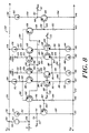
- FIG. 3 a schematic diagram of a magamp of the first embodiment of the A/D converter of the present invention is shown generally at 250.
- the analog inputs to magamp 1. 202 are input at the V IH and V IL inputs at 218 and 220, respectively, which are the differential inputs of the differential amplifier of the magamp. These analog inputs are input to the bases of bipolar npn transistors 250 and 252, respectively. These transistors form a differential input pair.
- the analog signals also are input to the V IH and V IL inputs to comparator 255 at 257 and 259, respectively.
- FIG. 1A the analog signals input to comparator 255 are shown in Figure 1A.
- the signals output from comparator 255 are used to drive the current switching transistors that includes npn transistors 280, 282, 284, and 286, as will be described.
- the differential input amplifier that includes bipolar npn transistors 250 and 252 connects between V CC 270 and V EE 272. Referring first to the first branch of the differential input amplifier that includes transistor 250, the emitter of transistor 250 connects to V EE through current source 262. The collector of transistor 250 connects to V CC 270 though transistor pair 280 and 284, and load resistors 310 and 318. Specifically, line 251 connects the collector of transistor 250 to node 290 in line 288, and line 288 connects to the emitters of transistors 280 and 284. Line 306 connects the collector of transistor 280 to V CC 270 at node 312. Load resistor 310 is disposed in line 306.
- the collector of transistor 284 connects to V CC 270 at node 320 via line 300, node 304, line 314, and load resistor 318.
- Line 300 connects the collector of transistor 284 to node 304.
- Node 304 is disposed in line 314.
- Line 314 connects the collector of transistor 282 to V CC 270 at node 320.
- Load resistor 318 is disposed in line 314 between node 304 and node 320 on V CC 270.
- Node 308 is disposed in line 306 that connects between the collector of transistor 280 and V CC 270 at node 312.
- Node 302 also is disposed in line 306.
- Line 298 connects node 302 to the collector of npn bipolar transistor 286. This transistor will be discussed subsequently.
- line 322 connects to node 308 and the base of bipolar npn transistor 324.
- Line 326 connects the collector of transistor 324 to V CC 270 at node 336.
- Line 328 connects the emitter of transistor 324 to V EE 272 at node 340.
- Current source 334 is disposed in line 328, and node 332 is disposed in line 328 between transistor 324 and current source 334.
- Line 333 connects between node 332 and the V OH output at 232.
- the emitter of input transistor 252 connects to V EE 272 at node 265 through current source 264.
- Line 258 connects between node 281 in line 243 and node 283 in line 285.
- Resistor 260 is disposed in line 258.
- Transistors 250 and 252, and resistor 260 operate conventionally for linear conversion of the analog inputs.
- the collector of transistor 252 connects to V CC 270 though transistor pair 282 and 286.
- Line 253 connects to the collector of transistor 252 connects to node 296 in line 297.
- Line 297 connects the emitters of transistors 282 and 286.
- line 314 connects the collector of transistor 282 to V CC 270 at node 320.
- Load resistor 318 is disposed in line 314.
- the collector of transistor 286 connects to V CC 270 at node 312 via line 298, node 302, line 306, and load resistor 310.
- Line 298 connects the collector of transistor 286 to node 302.
- Node 302 is disposed in line 306.
- Line 306 connects the collector of transistor 280 to V CC 270 at node 312.
- Load resistor 310 is disposed in line 306 between node 302 and node 312 on V CC 270.
- node 316 is disposed in line 314 that connects between the collector of transistor 282 and V CC 270 at node 320.
- node 304 also is disposed in line 314.
- Line 344 connects to node 316 and the base of bipolar npn transistor 246.
- Line 248 connects the collector of transistor 246 to V CC 270 at node 249.
- Line 267 connects the emitter of transistor 246 to V CC 270.
- Current source 273 is disposed in line 267 and node 269 is disposed in line 267 above current source 273.
- Offset resistor 330 is disposed in line 267 between node 269 and transistor 246. This resistor is used to align the signal, as shown in Figure 1C,
- Line 271 connects between node 269 and the V OL output at 234.
- the V OH and the V OL outputs are connected to the next magamp stage.
- Comparator 255 is shown in Figure 4.
- comparator 255 includes a differential input transistor pair, bipolar npn transistors 350 and 351.
- the V IH input at 257 connects to the base of transistor 350.
- Line 360 connects the collector of transistor 350 to V CC 270 at node 366.
- Load resistor 364 is disposed in line 360.
- the V IL input at 259 connects to the base of transistor 351.
- Line 388 connects the collector of transistor 351 to V CC 270 at node 394.
- Load resistor 392 is disposed in line 388.
- the emitters of input transistors 350 and 351 are coupled by line 352.
- Common node 353 is disposed in line 352.
- Line 354 connects common node 353 to V EE 272 at node 358.
- Current source 356 is disposed in line 354. This circuit operates conventionally.
- Node 362 is disposed in line 360 between the collector of transistor 350 and load resistor 364.
- Line 370 connects node 362 to the base of bipolar npn transistor 372.
- Line 374 connects the collector of transistor 372 to V CC 270 at node 376.
- Line 378 connects the emitter of transistor 372 to V EE 272 at node 384.
- Current source 382 is disposed in line 378.
- Node 380 is disposed in line 378 between transistor 372 and current source 382.
- Line 386 connects between node 380 and the B N output at 226 of comparator 255.
- Node 390 is disposed in line 388 between the collector of transistor 351 and load resistor 392.
- Line 396 connects node 390 to the base of bipolar npn transistor 398.
- Line 400 connects the collector of transistor 398 to V CC 270 at node 402.
- Line 404 connects the emitter of transistor 398 to V EE 272 at node 410.
- Current source 408 is disposed in line 404.
- Node 406 is disposed in line 404 between transistor 398 and current source 408.
- Line 412 connects between node 406 and the B output at 224 of comparator 255.
- the B signal of comparator 255 on line 276 connects to node 277 that is disposed in line 275.
- Line 275 connects to the bases of transistors 280 and 282 of the current switching transistors.
- the B N signal of comparator 255 on line 278 connects to node 292 that is disposed in line 294.
- Line 294 connects to the bases of transistors 284 and 286 of the current switching transistors.
- the current switching transistors are used to fold the input signals as shown, for example, in Figure 1B.
- the slew rate at V 1 and V 2 is zero, and the state of the comparator does not affect these signals. More specifically, when the V 1L and V 1H inputs are centered or equal, the output of comparator 255 is centered and there are equal currents in transistors 250 and 252. These currents are split evenly in transistors 280, 282 and 286 of the current switching circuit. These currents recombine in the load resistors 310 and 318. When one of the magamps of the system are in this state, they all can be latched in parallel.
- offset resistor 330 offsets the V 2 signal 1/2 full scale, as shown in Figure 1C.
- the offset is done after load resistors 310 and 318 to remove errors at mid-scale due to the early voltage effects of transistors 310 and 318 to remove errors at mid-scale due to the early voltage effects of transistors 280, 282, 284 and 286.
- the folded and offset signals (as shown in Figure 1C) are fed to the next stage magamp.
- the configuration of the circuit has output transistors 324 and 246. These transistors buffer load resistors 310 and 318 from the inputs of the next stage.
- the gain of the magamps is set by load resistors 310 and 318, resistor 260, and the dynamic resistance of transistors 250 and 252.
- the offset across resistor 330 is then set to 1/2 of the full scale output range. The circuit designer can select any desired gain for any magamp stage.
- magamp configuration of Figure 3 has the added advantage that the latching function is outside of the comparator and, therefore, outside of the analog path.
- the latch for the circuit is connected to the B signal output at 224 and the B N signal output at 226.
- Figures 5-8 are directed to a second embodiment of the serial-type A/D converter of the present invention.
- the elements of this second embodiment that are the same as elements of the first embodiment will have the same reference numbers.
- the second embodiment of the serial-type A/D converter of the present invention includes magamp 1,502, magamp 2,502, magamp 3,506, magamp n-1, 510, and comparator 508. All of the n-1 magamps of the second embodiment of the serial-type A/D converter of the present invention have substantially the same construction. Therefore, except as otherwise indicated, the description of magamp 1,502' applies equally to magamp 2,504, magamp 3, 506, and magamp n-1,510.
- Magamp 1,502 has two analog inputs. One analog signal is input to the V IH input at 218 and the other analog input is input to V IL at 220. These signals constitute a differential input to the magamp. Certain outputs of magamp 1,502, are input to magamp 2,504. Specifically, the signal output from the V OH output at 232 of magamp 1,502, is input to the V IH input of magamp 2,504, at 218, and, in like manner, the signal output from the V OL output at 234 of magamp 1,502, is input to the V IL input at 220 of magamp 2, 504.
- Magamp 1,502 has two reference inputs for setting the full scale input range.
- One reference input is the signal input to the V RIH input at 530 and the other is the signal input to the V RIL input at 532.
- Magamp 1, 502 also has two reference outputs which match the full scale range of the signals output from the V OH and V OL outputs at 232 and 234, respectively.
- One reference output is the signal at the V ROH output at 512 and the other is the signal at the V ROL output at 514.
- the signals output from the V ROH and V ROL outputs of one magamp stage connect to the V RIH and V RIL inputs of the next successive magamp stage, respectively.
- the n-1 magamps of the serial-type A/D converter of the present invention provides two differential outputs to Gray scale code-to-binary unit with outputs stages 212.
- the first differential output is the signals output from the B output at 224 and from the B N output at 226. These are the outputs from the comparator of the magamp unit before they are processed by the current switching transistors.
- the signals output from B and B N outputs are processed by Gray scale code-to-binary converter with output stages 212 to produce the n-bit parallel digital signal.
- magamp unit 520 is an inverted, cascoded amplifier that includes a current switching circuit.
- Reference unit 550 is used for setting the full-scale input range of magamp unit 520 and applying the reference signals to the next successive magamp stage.
- the inputs to magamp unit 520 are the analog signals input to the V IH and V IL inputs at 218 and 220, respectively. These are the differential inputs to magamp unit 520.
- One of the outputs of magamp unit 520 is the differential output that is input to Gray scale code-to-binary unit with output stage 212. This differential output is on line 540 that connects to the B output at 224 and is on line 542 that connects to the B N output at 226.
- Another differential output is on line 525 that connects to the V OH output at 232 and on line 527 that connects to the V OL output at 234.
- a differential signal connected to magamp unit 520 is the differential reference on lines 534 and 536.
- the signal on line 534 is the signal V 1 that is at node 522 and the signal on line 536 is the signal V 2 that is at node 524.
- the V 1 and V 2 nodes are used by the reference unit to supply offset currents to align the signals as shown in Figure 1C.
- the differential output of reference unit 550 is on lines 532 and 554.
- the output on line 532 is input to V ROH output at 512 and the V ROL output at 514. These are the reference voltage inputs to the next succession magamp stage.
- magamp unit 520 will be described, then reference unit 550 will be described.
- the analog inputs to magamp unit 520 are input to the V IH and V IL inputs at 218 and 220, respectively.
- This differential input is input to the bases of bipolar npn transistors 602 and 604 via lines 600 and 687, respectively.
- These analog inputs also are input to the V IH input at 630 and the V IL input at 632 of comparator 633.
- Comparator 633 like comparator 255 in Figure 3, receives the inputs just described and generates an output of a desired gain that is used to drive the current switching transistors that includes npn transistors 646, 648, 670, and 672.
- Bipolar npn transistors 602 and 604 are part of a differential input amplifier stage that connects between V CC 270 and V EE 272. Referring first to the first branch of the differential amplifier that includes input transistor 602, the emitter of input transistor 602 connects to V EE 272 at node 616 through current source 610. The collector of transistor 602 connects to V CC 270 at node 658 though transistor pair 646 and 648. Line 640 connects between the collector of transistor 602 and node 642 on line 644. Line 644 connects the emitters of transistors 646 and 648.
- Line 650 connects the collector of transistor 646 to V CC 270 at node 658.
- Current source 656 is disposed in line 650.
- Nodes 652 and 654 are disposed in line 650 below current source 656.
- the collector of transistor 648 connects to V CC 270 at node 682 via line 660, node 676, and line 674.
- Line 660 connects the collector of transistor 648 to node 676.
- Node 676 is disposed in line 674.
- Line 674 connects the collector of transistor 670 to V CC 270 at node 682.
- Current source 680 is disposed in line 674 above node 676.
- Node 678 is disposed in line 674 below current source 680.
- Node 652 is disposed in line 650.
- Line 650 connects between the collector of transistor 646 and V CC 270 at node 658.
- Line 684 connects node 652 to the collector of npn bipolar transistor 672. This transistor will be discuss subsequently.
- Node 654 also is disposed in line 650.
- Line 657 connects node 654 to node 524 that is common with reference unit 550.
- Line 700 connects to node 654 and to the emitter of bipolar pnp transistor 702.
- the collector of bipolar pnp transistor 702 is connected to line 706 that connects the collector to V EE 272 at node 712.
- Load resistor 710 is disposed in line 706.
- Node 708 is disposed in line 706 between the collector of bipolar pnp transistor 702 and load resistor 710.
- Line 714 connects node 708 to the base of bipolar pnp transistor 716.
- Line 720 connects the emitter of bipolar pnp transistor 716 to V CC 270 at node 724.
- Current source 722 is disposed in line 720.
- the collector of bipolar pnp transistor 716 is connected to V EE 272 at node 730 by line 728.
- Node 726 is disposed on line 720 between the emitter of bipolar pnp transistor 716 and current source 722.
- Line 525 connects this node to the V OH output at node 232.
- the emitter of input transistor 604 connects to V EE 272 at node 618 through current source 614.
- Line 612 makes this connection.
- Line 613 connects between node 617 in line 608 and node 619 in line 612.
- Resistor 615 is disposed in line 613.
- Transistors 602 and 604, and resistor 615 are used conventionally for linear conversion of the analog inputs.
- the collector of transistor 604 connects to V CC 270 at node 682 though transistor pair 670 and 672.
- Line 662 connects the collector of transistor 602 to node 664, and node 664 in disposed in line 668.
- the emitters of transistors 670 and 672 are connected to line 668.
- line 674 connects the collector of transistor 670 to V CC 270 at node 682.
- Current source 680 is disposed in line 674.
- the collector of transistor 672 connects to V CC 270 at node 658 via line 684, node 652, and line 650.
- Line 684 connects the collector of transistor 672 to node 652.
- Node 652 is disposed in line 650.
- Line 650 connects the collector of transistor 672 to V CC 270 at node 658.
- Node 652 connects to line 650 below current source 656.
- Node 678 is disposed in line 674.
- Line 679 connects node 678 to node 522 that is common with reference unit 550.
- Line 732 connects to node 678 and to the emitter of bipolar pnp transistor 734.
- the collector of bipolar pnp transistor 734 is connected to line 736 that connects this collector to V EE 272 at node 742.
- Load resistor 740 is disposed in line 736.
- Node 738 is disposed in line 736 between the collector of bipolar pnp transistor 734 and load resistor 740.
- Line 746 connects node 738 to the base of bipolar pnp transistor 748.
- Line 750 connects the emitter of bipolar pnp transistor 748 to V CC 270 at node 756.
- Current source 754 is disposed in line 750.
- the collector of bipolar pnp transistor 748 is connected by line 758 to V EE 272 at node 760.
- Node 752 is disposed on line 736 between the emitter of bipolar pnp transistor 734 and current source 754.
- Line 527 connects this node to the V OL output at node 234.
- transistors 702 and 734 are connected in an inverted, cascode manner, which helps increase the speed of the device and eliminate mid-scale errors due to the early voltage effects of transistors 646, 648, 672, and 670.
- reference unit 550 has two differential amplifiers.
- the first includes bipolar npn transistors 852 and 868 and is used for pulling the offset currents from node 522 carrying the V 1 signal and from node 524 carrying the V 2 signal.
- the second differential amplifier includes bipolar npn transistors 802 and 826 and is used for accurately referencing the full-scale output range of magamp unit 520.
- the V RIH input to reference unit 550 at node 530 connects to line 800. This line connects to the bases of bipolar npn transistors 802 and 852. In a similar manner, the V RIL input to reference unit 550 at node 532 connects to line 824. Line 824 connects to the bases of bipolar npn transistors 826 and 868.
- the differential amplifier that includes bipolar npn transistors 852 and 868 will be discussed, then the differential amplifier that includes bipolar npn transistors 802 and 826 will be discussed.
- the collector of bipolar npn transistor 852 connects to the emitter of bipolar npn transistor 856 via line 854.
- the collector of bipolar npn transistor 856 connects to node 522 carrying the V 1 signal via line 858.
- Line 860 connects to the emitter of bipolar npn transistor 852 to V EE 272 at node 866.
- Current source 864 is disposed in line 860.
- Node 862 is disposed in line 860 above current source 864.
- the collector of bipolar npn transistor 868 connects to the emitter of bipolar npn transistor 872 via line 870.
- the collector of bipolar npn transistor 872 connects to node 524 carrying the V 2 signal via line 874.
- Line 876 connects to the emitter of bipolar npn transistor 868.
- Line 876 connects to V EE 272 at node 882.
- Current source 880 is disposed in line 876.
- Node 878 is disposed in line 876 above current source 880.
- Node 862 in line 860 is connected to node 878 in line 876 by line 884.
- Resistor 886 is disposed in line 884.
- Transistors 852 and 868, and resistor 886 are used conventionally for linear conversion of the input signal to a differential output current.
- Line 888 connects to the bases of bipolar npn transistors 806, 830, 856, and 872. Node 890 is disposed in line 888. Line 892 connects nodes 890 and 894. This provides the appropriate bias voltage to bipolar npn transistors 806,830,856,872,898, and 926 so that they will conduct.
- the collector of bipolar npn transistor 802 is connected to the emitter of bipolar npn transistor 806 by line 804.
- Line 808 connects the collector of bipolar npn transistor 806 to node 814 in V CC 270.
- Current source 812 is disposed in line 808 and node 810 is disposed in line 808 below current source 812.
- bipolar npn transistor 802 connects to line 816. This line connects to V EE 272 at node 822.
- Current source 820 is disposed in line 816, and node 818 is disposed in line 816 above current source 820.
- Line 896 connects to node 810 and to the emitter of bipolar pnp transistor 898.
- the collector of bipolar pnp transistor 898 is connected to line 900 that connects the collector to V EE 272 at node 906.
- Load resistor 904 is disposed in line 900.
- Node 902 is disposed in line 900 between the collector of bipolar pnp transistor 898 and load resistor 904.
- Line 908 connects node 902 to the base of bipolar pnp transistor 910.
- Line 912 connects the emitter of bipolar pnp transistor 910 to V CC 270 at node 918.
- Current source 916 is disposed in line 912.
- the collector of bipolar pnp transistor 910 is connected to V EE 272 at node 922 by line 920.
- Node 914 is disposed on line 912 between the emitter of bipolar pnp transistor 910 and current source 916.
- Line 554 connects this node to the V ROL output at 514.
- the collector of bipolar npn transistor 826 is connected to the emitter of bipolar npn transistor 830 by line 828.
- Line 832 connects the collector of bipolar npn transistor 830 to node 838 in V CC 270.
- Current source 836 is disposed in line 832 and node 834 is disposed in line 832 below current source 836.
- bipolar npn transistor 826 connects to line 840. This line connects to V EE 272 at node 846.
- Current source 844 is disposed in line 840 and node 842 is disposed in line 840 above current source 844.
- Node 818 in line 816 is connected to node 842 in line 840 by line 848.
- Resistor 850 is disposed in line 848.
- Transistors 802 and 826, and resistor 850 are used conventionally for linear conversion of the input signals.
- Line 924 connects to node 834 in line 832 and to the emitter of bipolar pnp transistor 926.
- the collector of bipolar pnp transistor 926 is connected to line 928 that connects the collector to V EE 272 at node 933.
- Load resistor 932 is disposed in line 928.
- Node 930 is disposed in line 928 between the collector of bipolar pnp transistor 926 and load resistor 932.
- Line 934 connects node 930 to the base of bipolar pnp transistor 936.
- Line 938 connects the emitter of bipolar pnp transistor 936 to V CC 270 at node 944.
- Current source 942 is disposed in line 938.
- the collector of bipolar pnp transistor 936 is connected by line 946 to V EE 272 at node 948.
- Node 940 is disposed on line 938 between the emitter of bipolar pnp transistor 936 and current source 942.
- Line 552 connects this node to the V ROH output at 512.
- transistors 898 and 926 are connected in an inverted, cascode manner to properly match the gain of magamp unit 520.
- Line 704 connects to the bases of bipolar pnp transistors 898 and 926 in Figure 8 and bipolar pnp transistors 702 and 734 in Figure 7.
- the voltage on this line is derived from voltage source 952 in line 950.
- Line 950 connects between node 958 in line 704 and V CC 270 at node 954.
- magamp unit 520 and reference unit 550 when magamp unit 520 and reference unit 550 are in operation, the signals input to magamp unit 520 are as shown in Figure 1A and the output signals are as shown in Figure 1C.
- Magamp 1, 502 which is the second embodiment of the magamp of present invention, operates faster than the magamp, such as magamp 1, 202, of the first embodiment of the present invention because of the inverted, cascode transistors and the placement of the load resistors in the magamp unit 520. As such, there will be low impedance at node 654 for the V 2 signal and at node 678 for the V 1 signal of magamp unit 520, and low parasitic capacitance at nodes 708 and 738. This overall configuration therefore, greatly increases the speed of the device.
- magamp unit 520 and reference unit 550 operate as follows. Again referring to Figures 1A, 1C, 7, and 8, when the V IH input at 218 is LOW and the V IL input at 220 is HIGH, as shown in Figure 1A, the output of comparator 633 on line 540 for the B output is LOW and on line 542, the negative true output, for the B N output is HIGH. This will cause transistors 648 and 672 to conduct.
- the V 1 and V 2 signals at nodes 522 and 524, respectively, are input from reference unit 550. Through the differential amplifier that includes bipolar npn transistors 852, 868, 856.
- offset current is pulled from both sides of magamp unit 520 through nodes 522 and 524 for aligning the output signals.
- These offset currents are not pulled directly from the output of the differential amplifier so the problems that may be caused by it do not occur.
- the aligned signals are output for magamp unit 520 at the V OH output at 232 and the V OL output at 234. These outputs are input to the next magamp stage.
- the outputs of the reference unit amplifier, the V ROH and V ROL outputs, are the differential reference voltage for input to reference unit 550 of the next successive magamp. This will compensate for any gain errors in each magamp stage.
- the outputs of comparator 633 switch such that the B output on line 276 is HIGH and the B N output on line 278 is LOW . This will cause transistors 648 and 672 to stop conducting and transistors 646 and 670 to conduct. This also will result in the output lying on the folded curves for the V OH and V OL outputs, as shown in Figure 1C.
- magamp 502 operates is due to the position of load resistors in magamp unit 520 and the use of high speed bipolar pnp transistors in these units that are connected in an inverted, cascode manner.
- this configuration provides with respect to increasing speed in that it significantly reduces the parasitics at resistors 710 and 740.
- this configuration permits the circuit designer to select a desired gain for the magamp and not be restricted to a particular or accurate gain for which the half-scale offset must be compensated.
- magamp of the present invention includes the differential amplifier 1000A with current switching transistors ( Figure 9) and off-set circuitry 1000R ( Figure 10).
- the differential amplifier 1000A with current switching transistors ( Figure 9) will be discussed, then the offset circuitry 1000R ( Figure 10) will be discussed.
- the analog inputs to the differential amplifier 1000A are input to the V IH and V IL inputs at 218 and 220, respectively.
- the analog inputs are the input to the bases of bipolar npn transistors 1004 and 1008, respectively.
- the analog signals also are input to comparator 1098 at the V IH input at 1094 and V IL input at 1096.
- Bipolar npn transistors 1004 and 1008 are differential input transistors and connect between V CC 270 and V EE 272.
- the emitter of input transistor 1004 connects to V EE 272 through current source 1042.
- Node 1044 is disposed in line 1040 above current source 1042.
- the collector of transistor 1004 connects to V CC 270 though transistor pair 1016 and 1018 of the circuit switching transistors.
- Line 1010 connects the collector of transistor 1004 to node 1012 in line 1014.
- Line 1014 connects the emitters of transistors 1016 and 1018.
- Line 1022 connects the collector of transistor 1016 to V CC 270 at node 1030.
- Load resistor 1024 is disposed in line 1022.
- Nodes 1026 and 1028 are disposed in line 1022 below load resistor 1024.
- the collector of transistor 1018 connects to V CC 270 at node 1066 via line 1034, node 1064, line 1058, and load resistor 1060.
- Line 1034 connects the collector of transistor 1018 to node 1064.
- Node 1064 is disposed in line 1058.
- Line 1058 connects the collector of transistor 1054 to V CC 270 at node 1066.
- Load resistor 1060 is disposed in line 1058.
- Node 1064 connects to line 1058 below load resistor 1060.
- node 1026 is disposed in line 1022.
- Line 1036 connects between node 1026 and node 1038.
- the signal at node 1038 is the folded V 1 signal.
- node 1028 also is disposed in line 1022.
- Line 1032 connects node 1028 to the collector of npn bipolar transistor 1057. This transistor will be discussed subsequently.
- line 1082 connects the emitter of input transistor 1008 V EE 272 at node 1088 through current source 1084.
- Node 1086 is disposed in line 1082 above current source 1084.
- Line 1090 connects between nodes 1044 and 1086 in lines 1040 and 1082, respectively.
- Resistor 1092 is disposed in line 1090.
- Transistors 1004 and 1008, and resistor 1092 are used conventionally for linear conversion of the analog inputs.
- the collector of transistor 1008 connects to V CC 270 though transistor pair 1054 and 1057 of the current switching transistors.
- Line 1048 connects the collector of transistor 1008 to node 1050 in line 1052.
- Line 1052 connects the emitters of transistors 1054 and 1057.
- line 1058 connects the collector of transistor 1054 to V CC 270 at node 1066.
- Load resistor 1060 is disposed in line 1058.
- Nodes 1062 and 1064 are disposed in line 1058 below load resistor 1060.
- the collector of transistor 1057 connects to V CC 270 at node 1030 via line 1032, node 1028, line 1022, and load resistor 1024.
- Line 1032 connects the collector of transistor 1057 to node 1028. As stated, node 1028 is disposed in line 1022. Line 1022 connects the collector of transistor 1016 to V CC 270 at node 1030. Load resistor 1024 is disposed in line 1022. Node 1028 connects to line 1022 below load resistor 1024.
- node 1062 is disposed in line 1058.
- Line 1070 connects between node 1062 and node 1080.
- the signal at node 1080 is the folded V 2 signal.
- Comparator 1098 may be a conventional differential pair, such as the one shown in Figure 4. With respect to comparator 1098, the V IH input at 1094 receives the signal from node 218 and the V IL input at 1096 receives the signal at node 220.
- the B output of comparator 1098 on line 1100 connects to node 1102 that is disposed in line 1020.
- Line 1020 connects to the bases of transistors 1016 and 1054 of the current switching transistors.
- Node 1104 in line 1100 connects to node 224, which is the B output node.
- the B N output of comparator 1098 on line 1108 connects to node 1110 that is disposed in line 1056.
- Line 1056 connects to the bases of transistors 1018 and 1057 of the current switching transistors.
- Node 1112 in line 1108 connects to node 226, which is the B N output node.
- the signals at nodes 1038 and 1080 are the folded but offset as shown in Figure 1B.
- the offset circuit in Figure 10 will now be discussed. This circuit aligns the signals as shown in Figure 1C.
- the V RIH + signal is input at the V RIH input 1120. This signal is input to line 1122 that connects to the bases of bipolar npn transistors 1124 and 1180.
- the V RIL - signal is input at the V RIL input at node 1150. This signal is input to line 1152 that connects to the bases of bipolar npn transistors 1154 and 1192.
- the offset circuitry 100R has two differential amplifiers. The first includes transistors 1124 and 1154 and the second includes transistors 1180 and 1192. The first differential amplifier will be discussed, then the second will be discussed.
- line 1126 connects the collector of transistor 1124 to the emitter of bipolar npn transistor 1128.
- Load resistor 1132 is disposed in line 1126.
- Node 1134 is disposed in line 1126 below load resistor 1132 and node 1136 is disposed above load resistor 1131
- Line 1129 connects the collector of transistor 1128 to node 1130 on V CC 270.
- the emitter of transistor 1124 connects to line 1140 that connects to V EE 272 at node 1142.
- Current source 1144 is disposed in line 1140.
- Node 1146 is disposed in line 1140 above current source 1144.
- Line 1208 connects node 1134 in line 1126 to the V OL output at 1234.
- Line 1156 connects the collector of transistor 1154 to the emitter of bipolar npn transistor 1158.
- Load resistor 1162 is disposed in line 1156.
- Node 1166 is disposed in line 1156 below load resistor 1162 and node 1164 is disposed above load resistor 1162.
- Line 1159 connects the collector of transistor 1158 to node 1160 on V CC 270.
- Line 1210 connects node 1166 in line 1156 to the V OH output node at 1232.
- the emitter of transistor 1154 connects to line 1168 that connects to V EE 272 at node 1170.
- Current source 1172 is disposed in line 1168.
- Node 1174 is disposed in line 1168 above current source 1172.
- Line 1176 connects node 1146 in line 1140 to node 1174 in line 1168.
- Resistor 1178 is disposed in line 1178.
- Transistors 1124 and 1154, and resistor 1178 are used conventionally.
- the second differential amplifier that includes bipolar npn transistors 1180 and 1192. This amplifier is used to generate compensation currents for transistors 1128 and 1158.
- Line 1182 connects the collector of transistor 1180 to node 1164 in line 1156 above load resistor 1162. Node 1164 connects to the emitter of transistor 1158 via line -1156. The collector of transistor 1158 connects to V CC 270 at node 1160 via line 1159. Line 1184 connects the emitter of transistor 1180 to V EE 272 at node 1186. Current source 1188 is disposed in line 1184 and node 1190 is disposed in line 1184 above current source 1188.
- Line 1194 connects the collector of transistor 1192 to node 1136 in line 1126 above load resistor 1132.
- Node 1136 connects to the emitter of transistor 1128 via line 1126.
- the collector of transistor 1128 connects to V CC 270 at node 1130 via line 1128.
- Line 1196 connects the emitter of transistor 1192 to V EE 272 at node 1198.
- Current source 1200 is disposed in line 1196 and node 1202 is disposed in line 1196 above current source 1200.
- Line 1204 connects between node 1190 in line 1184 and node 1202 in line 1196.
- Resistor 1206 is disposed in line 1204.
- Transistors 1180 and 1192, and resistor 1206 are used conventionally.
- load resistors of the differential amplifier 1000A in Figure 9 and the load resistors in the offset circuitry 1000R in Figure 10 Preferably, if load resistors 1024 and 1060 of the differential amplifier has a value of R L , then load resistors 1162 and 1132 of the offset circuitry should have a value of R L / 2. Further, resistor 1092 of the differential amplifier should match resistors 1176 and 1206 of the differential pairs of the offset circuitry shown in Figure 10 and current sources 1042 and 1084 should match current sources 1188, 1144, 1172, and 1200.
- the offset circuitry in Figure 10 is used. This currently aligns the signals and establishes the full-scale input range of the magamp. The difference between the V RIH signal at node 1120 and the V RIL signal at node 1150 is equal the full-scale input range.
- the offset currents are generated through resistors 1132 and 1162 which result in the aligning of the signals output at the V OH output at node 1232and the V OL output at node 1234, as shown in Figure 1C.
- the currents generated by the differential pair comprised of transistors 1180 and 1192, and resistor 1206 compensate for the equal offset currents that flow through the emitters of transistors 1128 and 1158 and minimize offset errors.
- the folded and aligned signals are fed to the next magamp stage.
Landscapes
- Engineering & Computer Science (AREA)
- Power Engineering (AREA)
- Theoretical Computer Science (AREA)
- Analogue/Digital Conversion (AREA)
- Amplifiers (AREA)
Claims (12)
- A/D-Wandler (200) mit n-Bit vom seriellen Typ, der folgendes aufweist:dadurch gekennzeichnet, daß ein drittes und ein viertes Ausgangssignal (308, 316) von der Stromschalteinrichtung an Basiskontakte von Puffertransistoren (246, 324) geliefert werden, von denen jeder mit der einen Seite an einen Ausgangsanschluß (232, 234) angeschlossen ist, um ein gefaltetes Signal an einen nächsten Verstärker zu liefern.(n - 1) Verstärker (202, 204, 206, 210),n Komparatoren (288, 255), undeinen Gray-Code/Binär Darstellungs-Wandlerblock (212), wobei die (n - 1) Verstärker derart hintereinander geschaltet sind, daß ein Ausgangssignal des einen Verstärkers ein Eingangssignal für einen nächsten Verstärker liefert,wobei die Ausgangssignale der Komparatoren ein Differenzeingangssignal für den Gray-Code/Binär Darstellungs-Wandlerblock liefern, wobei jeder der Verstärker eine Differenzeingangsschaltung (250, 252) aufweist, um das analoge Differenzeingangssignal (VIH, VIL) zu empfangen und zu verstärken,wobei eine Stromschalteinrichtung (280, 282, 284, 286), vorgesehen ist, die an die Differenzeingangsschaltung angeschlossen ist, um das analoge Differenzeingangssignal zu falten,wobei ein Komparator (255) vorgesehen ist, der das analoge Differenzeingangssignal (VIH, VIL) empfängt und ein erstes und ein zweites Steuersignal (275) erzeugt, um die Stromschalteinrichtung (280, 282, 284, 286) zu steuern, undwobei ein erster und ein zweiter Ausgang (232, 234) vorgesehen sind, um ein erstes und ein zweites Ausgangssignal (VOH, VOL) zu liefern,
- Wandler nach Anspruch 1,
der ferner einen Widerstand (330) zwischen dem einen der Puffertransistoren (246) und dem Ausgangsanschluß (234) zum Abstimmen der gefalteten Signale aufweist, um gewünschte Kreuzungspunkte zwischen den gefalteten Signalen zu erzeugen. - Wandler nach Anspruch 1 oder 2,
wobei die Stromschalteinrichtung (280, 282, 284, 286) einen ersten, zweiten, dritten und vierten Schalttransistor aufweist, wobei der erste und der zweite Schalttransistor (280, 284) einen ersten Bereich der Stromschalteinrichtung bilden und der dritte und der vierte Schalttransistor (286, 282) einen zweiten Bereich der Stromschalteinrichtung bilden. - Wandler nach Anspruch 1,
wobei jeder Verstärker eine Verstärkereinheit (520) und eine Referenzeinheit (550) aufweist, wobei die Referenzeinheit Eingänge (VRIH, VRIL) zum Festlegen eines vollständigen Eingangsbereiches und Referenzausgänge (VROH, VROL) aufweist, die an einen vollständigen Bereich der Ausgangssignale angepaßt sind. - Wandler nach Anspruch 4,
wobei jede Referenzeinheit (550) eine zweite Differenzelngangsschaltung zum Empfangen und Verstärken eines Referenz-Differenzsignals und zum Liefern eines Offsetstromes an die Verstärkereinheit aufweist, um das erste und das zweite gefaltete Signal derart abzustimmen, daß ein Wert von dem einen des ersten und des zweiten gefalteten Signals relativ zu dem anderen geändert wird. - Wandler nach einem der vorstehenden Ansprüche,
der ferner einen Transistor (734) in invertierter Kaskodenschaltung aufweist, der zwischen den Puffertransistor (748) und die Stromschalteinrichtung (646, 648, 672, 670) geschaltet ist. - Wandler nach Anspruch 6,
- wobei der Transistor (734) in Kaskodenschaltung mit dem einen Anschluß (732) mit der Stromschalteinrichtung verbunden ist und mit einem anderen Anschluß (736) mit dem Steueranschluß (746) eines Ausgangstransistors (748) und ferner mit einem Lastwiderstand (740) verbunden ist. - Wandler nach einem der vorstehenden Ansprüche,
der die Referenzeinhelt (550) aufweist, die eine zweite Differenz-Elngangsschaltung aufweist, um ein entsprechendes Referenz-Dirferenzsignal zu empfangen, ein Offsetsignal zum Abstimmen des ersten und des zweiten Ausgangssignals zu liefern, und um der nächsten Stufe ein Referenz-Differenzausgangssignal zu liefern. - Wandler nach Anspruch 8,
wobei jede Referenzeinheit ein erstes und ein zweites Paar von Differenztransistoren aufweist, wobei das erste Paar das Referenz-Differenzausgangssignal und das zweite Paar das Offsetsignal liefert. - Wandler nach Anspruch 9,
wobei jede Referenzeinheit ein drittes Paar von Transistoren aufweist, wobei jeder Transistor in dem zweiten Paar von Transistoren an einer ersten Seite mit einem entsprechenden Transistor des dritten Paares von Transistoren und an einer zweiten Seite mit einer Stromquelle verbunden ist, wobei das dritte Paar von Transistoren mit der ersten und der zweiten Ausgangsschaltung verbunden ist. - Wandler nach einem der vorstehenden Ansprüche,
der die Referenzschaltung (550) aufweist, die mit Steueranschlüssen des ersten und des zweiten Puffertransistors verbunden ist, um diesen eine Vorspannung zu liefern. - Wandler nach einem der vorstehenden Ansprüche,
der ferner einen Verstärkerbereich (1000A) mit Lastwiderständen (1024, 1060) zwischen der Stromschalteinrichtung (1016, 1018, 1057, 1054) und einer Spannungsquelle (VCC) aufweist, wobei der Wandler ferner eine Offsetschaltungsanordnung (1000R) mit Lastwiderständen (1132, 1162) aufweist, die mit den Ausgangsanschlüssen (1232, 1234) verbunden sind, wobei die Lastwiderstände In der Offsetschaltungsanordnung den halben Widerstand der Lastwiderstände in dem Verstärkerbereich (1000A) aufweisen.
Applications Claiming Priority (3)
| Application Number | Priority Date | Filing Date | Title |
|---|---|---|---|
| US347909 | 1994-12-01 | ||
| US08/347,909 US5684419A (en) | 1994-12-01 | 1994-12-01 | n-bit analog-to-digital converter with n-1 magnitude amplifiers and n comparators |
| PCT/US1995/015467 WO1996017437A1 (en) | 1994-12-01 | 1995-11-29 | n-BIT CONVERTER WITH n-1 MAGNITUDE AMPLIFIERS AND n COMPARATORS |
Publications (2)
| Publication Number | Publication Date |
|---|---|
| EP0795235A1 EP0795235A1 (de) | 1997-09-17 |
| EP0795235B1 true EP0795235B1 (de) | 2002-11-13 |
Family
ID=23365808
Family Applications (1)
| Application Number | Title | Priority Date | Filing Date |
|---|---|---|---|
| EP95940069A Expired - Lifetime EP0795235B1 (de) | 1994-12-01 | 1995-11-29 | N-bit umsetzer mit n-1-grössenverstärkern und n-vergleichern |
Country Status (4)
| Country | Link |
|---|---|
| US (1) | US5684419A (de) |
| EP (1) | EP0795235B1 (de) |
| DE (1) | DE69528845T2 (de) |
| WO (1) | WO1996017437A1 (de) |
Families Citing this family (14)
| Publication number | Priority date | Publication date | Assignee | Title |
|---|---|---|---|---|
| US5801657A (en) * | 1997-02-05 | 1998-09-01 | Stanford University | Serial analog-to-digital converter using successive comparisons |
| US6362767B1 (en) * | 1999-03-22 | 2002-03-26 | The Board Of Trustees Of The Leland Stanford Junior University | Methods for simultaneous analog-to-digital conversion and multiplication |
| US6249153B1 (en) * | 1999-05-25 | 2001-06-19 | Micrel Incorporated | High slew rate input differential pair with common mode input to ground |
| US6163290A (en) * | 1999-07-13 | 2000-12-19 | Analog Devices, Inc. | Linearizing structures and methods for unity-gain folding amplifiers |
| US6172636B1 (en) | 1999-07-13 | 2001-01-09 | Analog Devices, Inc. | Linearizing structures and methods for adjustable-gain folding amplifiers |
| US6246353B1 (en) | 1999-09-13 | 2001-06-12 | Analog Devices, Inc. | Integrated-circuit structures and methods for correction of temperature and process-induced parameter errors |
| US6788237B1 (en) | 2001-03-30 | 2004-09-07 | Pixim, Inc. | Electrically and optically symmetrical analog-to-digital converter for digital pixel sensors |
| US6310571B1 (en) | 2001-03-30 | 2001-10-30 | Pixim, Incorporated | Multiplexed multi-channel bit serial analog-to-digital converter |
| US6693575B1 (en) * | 2001-03-30 | 2004-02-17 | Pixim, Inc. | Multi-channel bit-serial analog-to-digital converter with reduced channel circuitry |
| US6628167B1 (en) | 2002-10-23 | 2003-09-30 | The Boeing Company | Linearized folding amplifier |
| US8638125B2 (en) * | 2008-03-14 | 2014-01-28 | Texas Instruments Incorporated | Low voltage differential signal driver with reduced power consumption |
| CN102055474B (zh) * | 2009-10-28 | 2013-06-26 | 北京大学 | 折叠器、折叠插值型模/数转换器 |
| RU2458456C1 (ru) * | 2011-04-20 | 2012-08-10 | Государственное образовательное учреждение высшего профессионального образования "Южно-Российский государственный университет экономики и сервиса" (ГОУ ВПО "ЮРГУЭС") | Аналоговый смеситель двух сигналов |
| US8884655B2 (en) | 2013-04-11 | 2014-11-11 | Texas Instruments Incorporated | Low-power voltage mode high speed driver |
Family Cites Families (14)
| Publication number | Priority date | Publication date | Assignee | Title |
|---|---|---|---|---|
| DE1955555C3 (de) * | 1969-11-05 | 1979-03-29 | Licentia Patent-Verwaltungs-Gmbh, 6000 Frankfurt | Anelog/Digital-Umsetier für sehr hohe Frequenzen |
| GB1477842A (en) * | 1974-06-15 | 1977-06-29 | Micro Consultants Ltd | Analogue-to-digital converters |
| DE2645606A1 (de) * | 1976-10-08 | 1978-04-13 | Licentia Gmbh | Breitband-faltverstaerker, vornehmlich fuer a/d-wanddler |
| US4599602A (en) * | 1983-08-03 | 1986-07-08 | Matsushita Electric Industrial Co., Ltd. | Serial-type A/D converter utilizing folding circuit cells |
| JPS60172823A (ja) * | 1984-02-13 | 1985-09-06 | Nippon Telegr & Teleph Corp <Ntt> | 増幅器 |
| US4931797A (en) * | 1987-11-11 | 1990-06-05 | Matsushita Electric Industrial Co., Ltd. | Folding circuit and serial-type A/D converter |
| JPH04211508A (ja) * | 1990-06-15 | 1992-08-03 | Toshiba Corp | 積分回路 |
| JP2610361B2 (ja) * | 1990-07-19 | 1997-05-14 | 株式会社東芝 | 半導体集積回路 |
| US5126742A (en) * | 1990-11-06 | 1992-06-30 | Signal Processing Technologies, Inc. | Analog to digital converter with double folding interpolation circuitry |
| US5307067A (en) * | 1992-04-20 | 1994-04-26 | Matsushita Electric Industrial Co., Ltd. | Folding circuit and analog-to-digital converter |
| US5392045A (en) * | 1992-11-06 | 1995-02-21 | National Semiconductor Corporation | Folder circuit for analog to digital converter |
| JP2787641B2 (ja) * | 1992-12-22 | 1998-08-20 | 三菱電機株式会社 | 差動減算器回路およびa/d変換器 |
| US5399988A (en) * | 1994-01-14 | 1995-03-21 | Tektronix, Inc. | FT doubler amplifier |
| US5550492A (en) * | 1994-12-01 | 1996-08-27 | Analog Devices, Inc. | Analog to digital converter using complementary differential emitter pairs |
-
1994
- 1994-12-01 US US08/347,909 patent/US5684419A/en not_active Expired - Lifetime
-
1995
- 1995-11-29 EP EP95940069A patent/EP0795235B1/de not_active Expired - Lifetime
- 1995-11-29 WO PCT/US1995/015467 patent/WO1996017437A1/en not_active Ceased
- 1995-11-29 DE DE69528845T patent/DE69528845T2/de not_active Expired - Lifetime
Also Published As
| Publication number | Publication date |
|---|---|
| DE69528845D1 (de) | 2002-12-19 |
| US5684419A (en) | 1997-11-04 |
| WO1996017437A1 (en) | 1996-06-06 |
| DE69528845T2 (de) | 2003-09-18 |
| EP0795235A1 (de) | 1997-09-17 |
Similar Documents
| Publication | Publication Date | Title |
|---|---|---|
| EP0795235B1 (de) | N-bit umsetzer mit n-1-grössenverstärkern und n-vergleichern | |
| JP3098243B2 (ja) | 電界効果トランジスタ差動増幅器 | |
| US7253686B2 (en) | Differential amplifiers with enhanced gain and dynamic range | |
| US5554943A (en) | Analog to digital converter having a magnitude amplifier with an improved differential input amplifier | |
| US4686511A (en) | Subranging analog-to-digital converter with FET isolation circuit between subtraction node and LSB encoder | |
| US5410274A (en) | Single-ended and differential amplifiers with high feedback input impedance and low distortion | |
| JPH09512684A (ja) | 低電圧cmosコンパレータ | |
| EP0219682B1 (de) | Strom/Spannungswandlerschaltung | |
| CN117631740B (zh) | 一种差分参考电压产生电路及电子设备 | |
| WO1990013949A1 (en) | Input stage for flash a/d converter | |
| US4748420A (en) | Quadcomp amplifier | |
| CN116112018A (zh) | 比较器 | |
| JP2615269B2 (ja) | 差動増幅器のオフセット低減回路 | |
| US6778013B1 (en) | Buffer amplifier structures with enhanced linearity | |
| JPH05217395A (ja) | サンプル−ホールド回路 | |
| US4692738A (en) | Analog signal processing apparatus | |
| US6172636B1 (en) | Linearizing structures and methods for adjustable-gain folding amplifiers | |
| US5757234A (en) | Feedforwrd differential amplifier | |
| Miki et al. | A 10-b 50 MS/s 500-mW A/D converter using a differential-voltage subconverter | |
| US5550492A (en) | Analog to digital converter using complementary differential emitter pairs | |
| US7012464B2 (en) | Method and circuit for a dual supply amplifier | |
| US6686864B1 (en) | Pipelined analog-to-digital converters with gain-matching structures | |
| US20070241818A1 (en) | Class ab folded cascode stage and method for low noise, low power, low-offset operational amplifier | |
| US6163290A (en) | Linearizing structures and methods for unity-gain folding amplifiers | |
| US5673047A (en) | Gain-compensating differential reference circuit |
Legal Events
| Date | Code | Title | Description |
|---|---|---|---|
| PUAI | Public reference made under article 153(3) epc to a published international application that has entered the european phase |
Free format text: ORIGINAL CODE: 0009012 |
|
| 17P | Request for examination filed |
Effective date: 19970701 |
|
| AK | Designated contracting states |
Kind code of ref document: A1 Designated state(s): DE FR GB |
|
| 17Q | First examination report despatched |
Effective date: 20000225 |
|
| GRAG | Despatch of communication of intention to grant |
Free format text: ORIGINAL CODE: EPIDOS AGRA |
|
| GRAG | Despatch of communication of intention to grant |
Free format text: ORIGINAL CODE: EPIDOS AGRA |
|
| GRAH | Despatch of communication of intention to grant a patent |
Free format text: ORIGINAL CODE: EPIDOS IGRA |
|
| GRAH | Despatch of communication of intention to grant a patent |
Free format text: ORIGINAL CODE: EPIDOS IGRA |
|
| GRAA | (expected) grant |
Free format text: ORIGINAL CODE: 0009210 |
|
| AK | Designated contracting states |
Kind code of ref document: B1 Designated state(s): DE FR GB |
|
| REG | Reference to a national code |
Ref country code: GB Ref legal event code: FG4D |
|
| REF | Corresponds to: |
Ref document number: 69528845 Country of ref document: DE Date of ref document: 20021219 |
|
| ET | Fr: translation filed | ||
| PLBE | No opposition filed within time limit |
Free format text: ORIGINAL CODE: 0009261 |
|
| STAA | Information on the status of an ep patent application or granted ep patent |
Free format text: STATUS: NO OPPOSITION FILED WITHIN TIME LIMIT |
|
| 26N | No opposition filed |
Effective date: 20030814 |
|
| PGFP | Annual fee paid to national office [announced via postgrant information from national office to epo] |
Ref country code: FR Payment date: 20131108 Year of fee payment: 19 |
|
| PGFP | Annual fee paid to national office [announced via postgrant information from national office to epo] |
Ref country code: DE Payment date: 20150218 Year of fee payment: 20 |
|
| PGFP | Annual fee paid to national office [announced via postgrant information from national office to epo] |
Ref country code: GB Payment date: 20150218 Year of fee payment: 20 |
|
| REG | Reference to a national code |
Ref country code: FR Ref legal event code: ST Effective date: 20150731 |
|
| REG | Reference to a national code |
Ref country code: DE Ref legal event code: R071 Ref document number: 69528845 Country of ref document: DE |
|
| PG25 | Lapsed in a contracting state [announced via postgrant information from national office to epo] |
Ref country code: FR Free format text: LAPSE BECAUSE OF NON-PAYMENT OF DUE FEES Effective date: 20141201 |
|
| REG | Reference to a national code |
Ref country code: GB Ref legal event code: PE20 Expiry date: 20151128 |
|
| PG25 | Lapsed in a contracting state [announced via postgrant information from national office to epo] |
Ref country code: GB Free format text: LAPSE BECAUSE OF EXPIRATION OF PROTECTION Effective date: 20151128 |