EP0789395A2 - Semiconductor device having capacitor and manufacturing method therefor - Google Patents
Semiconductor device having capacitor and manufacturing method therefor Download PDFInfo
- Publication number
- EP0789395A2 EP0789395A2 EP97106056A EP97106056A EP0789395A2 EP 0789395 A2 EP0789395 A2 EP 0789395A2 EP 97106056 A EP97106056 A EP 97106056A EP 97106056 A EP97106056 A EP 97106056A EP 0789395 A2 EP0789395 A2 EP 0789395A2
- Authority
- EP
- European Patent Office
- Prior art keywords
- film
- dielectric film
- resist pattern
- forming
- capacitor
- Prior art date
- Legal status (The legal status is an assumption and is not a legal conclusion. Google has not performed a legal analysis and makes no representation as to the accuracy of the status listed.)
- Granted
Links
Images

Classifications
-
- H—ELECTRICITY
- H01—ELECTRIC ELEMENTS
- H01L—SEMICONDUCTOR DEVICES NOT COVERED BY CLASS H10
- H01L27/00—Devices consisting of a plurality of semiconductor or other solid-state components formed in or on a common substrate
- H01L27/02—Devices consisting of a plurality of semiconductor or other solid-state components formed in or on a common substrate including semiconductor components specially adapted for rectifying, oscillating, amplifying or switching and having at least one potential-jump barrier or surface barrier; including integrated passive circuit elements with at least one potential-jump barrier or surface barrier
- H01L27/04—Devices consisting of a plurality of semiconductor or other solid-state components formed in or on a common substrate including semiconductor components specially adapted for rectifying, oscillating, amplifying or switching and having at least one potential-jump barrier or surface barrier; including integrated passive circuit elements with at least one potential-jump barrier or surface barrier the substrate being a semiconductor body
- H01L27/06—Devices consisting of a plurality of semiconductor or other solid-state components formed in or on a common substrate including semiconductor components specially adapted for rectifying, oscillating, amplifying or switching and having at least one potential-jump barrier or surface barrier; including integrated passive circuit elements with at least one potential-jump barrier or surface barrier the substrate being a semiconductor body including a plurality of individual components in a non-repetitive configuration
- H01L27/0611—Devices consisting of a plurality of semiconductor or other solid-state components formed in or on a common substrate including semiconductor components specially adapted for rectifying, oscillating, amplifying or switching and having at least one potential-jump barrier or surface barrier; including integrated passive circuit elements with at least one potential-jump barrier or surface barrier the substrate being a semiconductor body including a plurality of individual components in a non-repetitive configuration integrated circuits having a two-dimensional layout of components without a common active region
- H01L27/0617—Devices consisting of a plurality of semiconductor or other solid-state components formed in or on a common substrate including semiconductor components specially adapted for rectifying, oscillating, amplifying or switching and having at least one potential-jump barrier or surface barrier; including integrated passive circuit elements with at least one potential-jump barrier or surface barrier the substrate being a semiconductor body including a plurality of individual components in a non-repetitive configuration integrated circuits having a two-dimensional layout of components without a common active region comprising components of the field-effect type
- H01L27/0629—Devices consisting of a plurality of semiconductor or other solid-state components formed in or on a common substrate including semiconductor components specially adapted for rectifying, oscillating, amplifying or switching and having at least one potential-jump barrier or surface barrier; including integrated passive circuit elements with at least one potential-jump barrier or surface barrier the substrate being a semiconductor body including a plurality of individual components in a non-repetitive configuration integrated circuits having a two-dimensional layout of components without a common active region comprising components of the field-effect type in combination with diodes, or resistors, or capacitors
-
- H—ELECTRICITY
- H01—ELECTRIC ELEMENTS
- H01L—SEMICONDUCTOR DEVICES NOT COVERED BY CLASS H10
- H01L27/00—Devices consisting of a plurality of semiconductor or other solid-state components formed in or on a common substrate
- H01L27/02—Devices consisting of a plurality of semiconductor or other solid-state components formed in or on a common substrate including semiconductor components specially adapted for rectifying, oscillating, amplifying or switching and having at least one potential-jump barrier or surface barrier; including integrated passive circuit elements with at least one potential-jump barrier or surface barrier
- H01L27/04—Devices consisting of a plurality of semiconductor or other solid-state components formed in or on a common substrate including semiconductor components specially adapted for rectifying, oscillating, amplifying or switching and having at least one potential-jump barrier or surface barrier; including integrated passive circuit elements with at least one potential-jump barrier or surface barrier the substrate being a semiconductor body
- H01L27/06—Devices consisting of a plurality of semiconductor or other solid-state components formed in or on a common substrate including semiconductor components specially adapted for rectifying, oscillating, amplifying or switching and having at least one potential-jump barrier or surface barrier; including integrated passive circuit elements with at least one potential-jump barrier or surface barrier the substrate being a semiconductor body including a plurality of individual components in a non-repetitive configuration
- H01L27/0688—Integrated circuits having a three-dimensional layout
-
- H—ELECTRICITY
- H01—ELECTRIC ELEMENTS
- H01L—SEMICONDUCTOR DEVICES NOT COVERED BY CLASS H10
- H01L28/00—Passive two-terminal components without a potential-jump or surface barrier for integrated circuits; Details thereof; Multistep manufacturing processes therefor
- H01L28/40—Capacitors
-
- H—ELECTRICITY
- H01—ELECTRIC ELEMENTS
- H01L—SEMICONDUCTOR DEVICES NOT COVERED BY CLASS H10
- H01L28/00—Passive two-terminal components without a potential-jump or surface barrier for integrated circuits; Details thereof; Multistep manufacturing processes therefor
- H01L28/40—Capacitors
- H01L28/55—Capacitors with a dielectric comprising a perovskite structure material
-
- H—ELECTRICITY
- H10—SEMICONDUCTOR DEVICES; ELECTRIC SOLID-STATE DEVICES NOT OTHERWISE PROVIDED FOR
- H10B—ELECTRONIC MEMORY DEVICES
- H10B12/00—Dynamic random access memory [DRAM] devices
- H10B12/01—Manufacture or treatment
- H10B12/02—Manufacture or treatment for one transistor one-capacitor [1T-1C] memory cells
- H10B12/03—Making the capacitor or connections thereto
-
- H—ELECTRICITY
- H10—SEMICONDUCTOR DEVICES; ELECTRIC SOLID-STATE DEVICES NOT OTHERWISE PROVIDED FOR
- H10B—ELECTRONIC MEMORY DEVICES
- H10B53/00—Ferroelectric RAM [FeRAM] devices comprising ferroelectric memory capacitors
-
- H—ELECTRICITY
- H10—SEMICONDUCTOR DEVICES; ELECTRIC SOLID-STATE DEVICES NOT OTHERWISE PROVIDED FOR
- H10B—ELECTRONIC MEMORY DEVICES
- H10B53/00—Ferroelectric RAM [FeRAM] devices comprising ferroelectric memory capacitors
- H10B53/30—Ferroelectric RAM [FeRAM] devices comprising ferroelectric memory capacitors characterised by the memory core region
Definitions
- the present invention relates to a semiconductor device having capacitor employing a dielectric film and its manufacturing method.
- nonvolatile random access memory in simple constitution comprising a capacitor using a ferroelectric film, and dynamic random access memory using a capacitor made of dielectric film of high dielectric constant as a holding capacity are being developed.
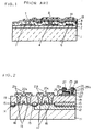
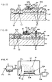
- Fig. 1 is a partially sectional view of a representative semiconductor device.
- reference number 1 denotes a semiconductor substrate, and the integrated circuit formed on the semiconductor substrate 1 is omitted in the drawing.
- An insulating film 2 is formed on the semiconductor substrate 1.
- metal interconnections 3, 4, 5 made of aluminum or aluminum alloy are formed.
- an insulating film 6 is formed, and a bottom electrode 9, a ferroelectric film 10, and a top electrode 11 are formed on the insulating film 6, and the bottom electrode 9 is connected to the metal interconnection 4 through a contact hole 8, and the top electrode 10 to the metal interconnection 3 through a contact hole 7.
- a capacitor comprising the bottom electrode 9, ferroelectric film 10 and top electrode 11 is inserted between the bias line Vss and bias line Vdd.
- a manufacturing method of the conventional semiconductor device having capacitor shown in Fig. 1 is described below.
- a metal film of aluminum or aluminum alloy is formed by sputtering or other method.
- This metal film is etched by ordinary photoetching method, and the metal interconnections 3, 4, 5 are formed. Consequently, on the entire surface of the semiconductor substrate 1, the insulating film 6 is formed by CVD method, and the contact holes 7,8 are formed in specified areas of the insulating film 6 by photoetching method.
- a metal film is then formed on the insulating film 6, and this metal film is photoetched to form the bottom electrode 9. Including the upper part of the bottom electrode 9, the ferroelectric film 10 is formed by sputtering. After removing the ferroelectric film 10 in the contact hole 7, an aluminum film or aluminum alloy film is formed, and the top electrode 11 is formed by photoetching.
- the metal interconnections 3, 4, 5 have been already formed when forming the ferroelectric film 10, and a part of the metal interconnections 3, 4, 5 is contacting with the diffusion layer (not shown in Fig. 1) of the semiconductor substrate 1, and therefore the ferroelectric film 10 cannot be treated at high temperature. That is, when the metal interconnections 3, 4, 5 are aluminum and the semiconductor substrate 1 is a silicon substrate, when heated at 450 °C or higher, aluminum may invade into the diffusion layer in spikes to penetrate through the diffusion layer.
- the bottom electrode 9 is formed, and then ferroelectric film 10 is formed thereon. Therefore, at the time of heat treatment of ferroelectric film 10, the reaction product due to reaction between ferroelectric film 10 and metal interconnection 3 is formed in the bottom of the contact hole 7. This reaction product is left over also when removing the ferroelectric film 10, which may cause contact failure between the metal interconnection 3 and top electrode 11.
- both ferroelectric film 10 and insulating film 6 must be etched, but the etchant satisfying the both etching conditions differs, and the process is complicated.
- a capacitor made of bottom electrode, dielectric film, and top electrode is formed on an insulating film of an integrated circuit, and the top electrode and bottom electrode of this capacitor are connected with the metal interconnections of the integrated circuit through the contact holes provided in a protective film formed to cover the capacitor.
- the capacitor since the capacitor is formed in a state independent from the integrated circuit, and the bottom electrode may be made of an optimum material selected in the relation with the dielectric film and the insulating film beneath the bottom electrode. Therefore, a favorable capacitor being small in fluctuation of the capacity may be formed.
- the dielectric film can be heated at a sufficiently high temperature, and a dielectric film with a large dielectric constant may be formed.
- the first contact hole provided in the insulating film formed on the substrate and the second contact hole provided on the insulating film formed to protect the capacitor can be formed, and the metal interconnections can be formed right after forming the contact holes, the inside of the contact holes will not be contaminated, and a favorable electric contact may be easily realized.
- the dielectric film is formed in a pattern, and therefore the contact holes can be formed only by etching the nitride film or oxide film used in the ordinary semiconductor device, so that the manufacturing process is not complicated.
- Fig. 1 is a partially sectional view showing the structure of essential parts of a conventional semiconductor device having capacitor.
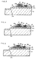
- Fig. 2 is a partially sectional view showing the structure of essential parts of a semiconductor device having capacitor in Embodiment 1 of the invention.
- Fig. 3 is a partially sectional view showing the structure of a capacitor of a semiconductor device in Embodiment 2 of the invention, in which the end of the top electrode of this semiconductor is formed at a position distant from the end of the bottom electrode.
- Fig 4 is a partially sectional view showing the structure of a capacitor of a semiconductor device modified from Embodiment 2, in which the dielectric film of this semiconductor device is formed beyond the end of the bottom electrode.
- Fig. 5 is a partially sectional view showing the structure of a capacitor of other semiconductor device modified from Embodiment 2, in which the end of the top electrode of this semiconductor device is located between the slope part in the step of the substrate and the end of the bottom electrode.
- Fig. 6 is a partially sectional view showing the structure of a capacitor of a semiconductor device in Embodiment 3 of the invention, in which the top electrode and metal interconnections of the semiconductor device are connected through a conductive film mainly composed of titanium being formed as containing contact holes.
- Fig. 7 is a sectional view showing the structure of a capacitor of a semiconductor device modified from Embodiment 3, in which the top electrode and metal interconnections are connected through a conductive film mainly composed of titanium being formed on the top electrode.
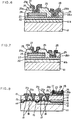
- Fig. 8 is a partially sectional view showing the structure of a semiconductor device in Embodiment 4 of the invention, in which the contact hole leading to the top electrode formed on the insulating film for protecting the capacitor is formed at a position not overlapping with the bottom electrode.
- Fig. 9 through Fig. 16 are partially sectional views showing a manufacturing method of a semiconductor device having capacitor in the invention, Fig. 9 being a diagram showing the state of forming a conductive film as bottom electrode, Fig. 10 showing the state of forming the dielectric film, Fig. 11 showing the state of forming a conductive film as top electrode, Fig, 12 showing the state of forming the top electrode and dielectric film, Fig. 13 showing the state of forming the bottom electrode and the state of removing the residue of the dielectric film, Fig. 14 showing the state of forming a protective film for protecting the capacitor, Fig. 15 showing the state of forming contact holes in the protective film and inter layer insulating film, and Fig. 16 showing the state of forming the metal interconnections.
- Fig. 17 is a schematic diagram of a forming apparatus of dielectric film in the manufacturing method of semiconductor device having capacitor of the invention.
- reference number 11 is an N-type silicon substrate, and on this N-type silicon substrate 11 are formed a P-type well 12, an isolation region 13 for isolating circuit elements in the P-type well 12, an isolation region 14 for isolating circuit elements in the silicon substrate 11, an isolating oxide film 15 composed of a thick silicon oxide film, a gate electrode 16, and an N-type diffusion layer 17 and a P-type diffusion layer 18 forming a transistor.
- Reference number 19 is an interlayer insulating film composed of silicon oxide film or the like formed on the N-type silicon substrate 11, and contact holes 20a, 20b are formed in this interlayer insulating film 19.
- metal interconnections 21a, 21b made of aluminum or aluminum alloy are formed through the contact holes 20a, 20b, and they are connected to the N-type diffusion layer 17 and P-type diffusion layer 18.
- a capacitor composed of a bottom electrode 22 such as platinun film, a dielectric film 23 possessing a high dielectric constant such as Ba 1-x Sr x TiO 3 (0 ⁇ X ⁇ 1), and a top electrode 24 of platinum or the like, and a protective film 25 such as silicon oxide film and silicon nitride film is formed on this capacitor.
- contact holes 26a, 26b are formed, and metal interconnections 27, 28 made of aluminum or aluminum alloy to be connected with the top electrode 24 and bottom electrode 22 respectively through contact holes 26a, 26b are formed on the protective film, 25.
- the capacitor is formed on the interlayer insulating film 19 independently of the integrated circuit formed on the silicon substrate 11, and after heat treatment of the dielectric film 23, the metal interconnections 21a, 21b, 27 and 28 are formed, and therefore the material for the bottom electrode 22 may be selected from a wide range. That is, the material for the bottom electrode 22 may be selected only in the relation with the interlayer insulating film 19 and dielectric film 23. Moreover, since the dielectric film 23 is heated before the metal interconnections 21a, 21b, 27 and 28 are formed, the dielectric film 23 can be treated at a higher temperature than the alloy temperature of aluminum and silicon. Therefore, as compared with the prior art, the dielectric film 23 excellent in electric characteristics may be obtained.
- the temperature of heat treatment for improving the interface of the metal interconnection 21a and N-type diffusion layer 17 and the interface between the metal interconnection 21b and the P-type diffusion layer 17 may be same as in the manufacturing condition of ordinary integrated circuit (450 °C, or less), and the process supplemented in order to incorporate the capacitor will not deteriorate the integrated circuit.
- transistors and other circuit elements for composing the integrated circuits are formed on a silicon substrate 31 aside from the capacitor, but the transistors and other parts not related directly with the explanation of Embodiment 2 and its modified semiconductor devices are not shown in the drawings.
- the silicon substrate 31 has a step 31a which is formed in the process of forming the integrated circuit, and an interlayer insulating film 31b such as silicon oxide film is formed on the surface of the silicon substrate 31.
- the capacitor is formed on this interlayer insulating film 31b.
- the capacitor is composed of a bottom electrode 22 such as platinum film, a dielectric film 23 possessing a high dielectric constant such as Ba 1-x Sr x TiO 3 (0 ⁇ X ⁇ 1), and a top electrode 24 such as platinum film.
- a protective film 25 such as silicon oxide film and silicon nitride film.
- Contact holes 26a, 26b are formed in the protective film 25 of the capacitor, and metal interconnections 27 and 28 made of aluminum or aluminum alloy to be connected to the top electrode 24 and bottom electrode 22 respectively are formed in the contact holes 26a, 26b.
- any structure it is configured so that the end of the bottom electrode 22 and the end of the top electrode 24 may be at distant positions.
- stress due to thermal expansion of the bottom electrode and top electrode 24 generated at the time of heat treatment of the dielectric film 23 is dispersed and lessened, and cracking of the dielectric film 23 and interlayer insulating film 31b can be prevented, so that the reliability may be improved.
- transistors and other circuit elements for composing the integrated circuits are formed on a silicon substrate 41 aside from the capacitor, but the other parts not related directly with the explanation of Embodiment 3 and its modified semiconductor devices are not shown in the drawings.
- the silicon substrate 41 has an interlayer insulating film 41b such as silicon oxide film formed thereon, and a capacitor is formed on this interlayer insulating film 41b.
- the capacitor is composed of a bottom electrode 22 such as platinum film, a dielectric film 23 possessing a high dielectric constant such as Ba 1-x Sr x TiO 3 (0 ⁇ X ⁇ 1), and a top electrode 24 such as platinum film.
- a protective film 25 such as silicon oxide film and silicon nitride film.
- Contact holes 26a, 26b are formed in the protective film 25 of the capacitor, and through these contact holes 26a, 26b, the top electrode 24 and bottom electrode 22, and metal interconnections 27 and 28 made of aluminum or aluminum alloy are connected mutually through conductive films 29a and 29b mainly composed of titanium.
- the conductive film 29a, 29b mainly composed of titanium are formed on the protective film 25 including the contact holes 26a, 26b, and through these conductive films 29a, 29b, the metal interconnection 27 is connected to the top electrode 24 and the metal interconnection 28 to the bottom electrode 22.
- the conductive film 29a mainly composed of titanium is formed on the top electrode 24, and the metal interconnection 27 is connected to the top electrode 24 through the conductive film 29a, and the metal interconnection 28 is directly connected to the bottom electrode 22.
- the conductive film 29a mainly composed of titanium adheres tightly with the top electrode 24 and protective film 25, separation does not occur between the top electrode 24 and protective film 25 in heat treatment of the dielectric film 23 or in heat treatment of the metal interconnections 27, 28.
- Fig. 8 shows a semiconductor device modified from Embodiment 1.
- a capacitor is formed on the interlayer insulating film 19, and in this case the dielectric film 23 and the top electrode 24 are formed beyond the end of the bottom electrode 22. Furthermore, to connect the top electrode 24 and metal interconnection 27, a contact hole 26a provided in the protective film 25 of the capacitor is formed at a position not overlapping with the bottom electrode 22. The capacitor is formed in an overlapped region of the bottom electrode 22 and top electrode 24 through dielectric film 23, and therefore effects applied on the capacitor when forming the contact holes 26a, 26b and top electrode 27 are small, and the reliability is improved.
- Figs. 9 through 16 are drawings to explain an example of manufacturing method of semiconductor device having capacitor according to the invention.
- an isolating oxide film 52 composed of a thick silicon oxide film for isolating a transistor region
- a gate electrode 53 composed of polycrystalline silicon film
- a conductor wiring 54 composed of polycrystalline silicon film
- a diffusion layer 55 and an interlayer insulating film 56 composed of silicon oxide film.
- the surface of the interlayer insulating film 56 is undulated due to effects of the gate electrode 53 and conductor wiring 54 formed beneath the interlayer insulating film 56.
- a multilayer film consisting of a titanium film 57 and a platinum film 57b is formed as a bottom electrode 57.
- a dielectric film 58a possessing a high dielectric constant such as Ba 1-x Sr x TiO 3 (0 ⁇ X ⁇ 1) is coated by means known in the art, and is heated.
- a platinum film 59a is formed as a top electrode 59.
- a resist pattern 60 is formed on the platinum film 59a, and using this resist pattern 60 as mask, the platinum film 59a and dielectric film 58a are etched sequentially, and the top electrode 59 and dielectric film 58 are formed.
- the residue 58b of the dielectric film 58 is often left over in the recess of the interlayer insulating film 56, and when this residue 58b is left over, contact failure may occur when forming contact holes 64a, 64b in a later process.
- a resist pattern 61 is newly formed on the platinum electrode 57b so as to cover the capacitor, and the platinum film 57b and titanium film 57a are etched by using this resist pattern 61 as mask, thereby forming the bottom electrode 57. Further using the resist pattern 61 as mask, the residue 58b of the dielectric film 58a is removed.
- a protective film 62 is formed on the entire upper surface of the silicon substrate 51.
- a contact hole 63a leading to the top electrode 59 and a contact hole 63b leading to the bottom electrode 57 are formed, and in the protective film 62 and interlayer insulating film 56 in the region other than the capacitor, a contact hole 64a leading to the diffusion layer 55 and a contact hole 64b leading to the conductor wiring 54 are formed, respectively.
- the contact holes 63a, 63b, and the contact holes 64a, 64b may be formed simultaneously in the same process, or in different processes.
- an aluminum film or an aluminum alloy film is formed on the entire surface of the silicon substrate 51, and the metal interconnections 65a, 65b, 66 and 67 are formed in the ordinary photoetching process.
- the process for removing the residue 58b explained in Fig. 13 may be omitted if the residue 58b has been sufficiently removed in the process in Fig. 12.
- the titanium film 57a and platinum film 57b for the bottom electrode 57, the dielectric film 58a, and the platinum 59a for the top electrode 59 are preliminarily laminated, then the top electrode 59 and dielectric film 58 are formed, and finally the bottom electrode 57 is formed, but a same excellent capacitor can be formed by varying the sequence of manufacturing process as follows.
- a multilayer film consisting of titanium film 57a and platinum film 57b to compose the bottom layer 57 is formed on this multilayer film.
- a first resist pattern is formed, and using this first resist pattern as mask, the multilayer film is etched, and the bottom electrode 57 is formed.
- the dielectric film 58a and the platinum film 59a for forming the top electrode 59 are formed sequentially on the silicon substrate 51.
- a second resist pattern is formed on the platinum film 59a, and using this second resist pattern as mask, the platinum film 59a and dielectric film 58a are etched, and the top electrode 59 and dielectric film 58 are formed.
- the protective film 62 is formed on the entire surface.
- a third resist pattern for covering the entire capacitor is formed, and using this third resist pattern as mask, the residue 58b of the dielectric film 58 left over in the other regions than the capacitor is removed.
- contact holes 63a, 63b, 64a, 64b are formed in the protective film 62 and interlayer insulating film 56. Consequently, on the entire surface of the silicon substrate 51, an aluminum film or an alloy film mainly composed of aluminum is forced, and the metal interconnections 65a, 65b, 66 and 67 are formed by ordinary photoetching process.
- Fig. 17 is a schematic diagram of a dielectric film forming apparatus in an embodiment of the invention, and this dielectric film forming apparatus is explained herein, together with the forming method of dielectric film in individual embodiments.
- reference number 71 is a pulverization chamber
- 72 is a film growth chamber
- 73 is an exhaust pump
- 74 particulates The pulverization chamber 71 comprises means 71a for pulverizing the material for composing the dielectric film, and a gas feed port 71b for feeding carrier gas.
- the pulverization chamber 71 and film growth chamber 72 are connected with a pipe 71c for feeding particulates 74 into the film growth chamber 72 together with carrier gas.
- the film growth chamber 72 comprises a substrate holder 72a for holding the substrate 75, a grid electrode 72b disposed above the substrate holder 72a, and an injection port 72c for injecting particulates 74 into the film growth chamber 72.
- the film growth chamber 71 and exhaust pump 73 are connected with an exhaust pipe 73a.
- the particultes 74 produced in the pulverization chamber 71 are injected into the film growth chamber 72 reduced in pressure by the exhaust pump 73 through the injection port 72c.
- the particulates 74 when pulverized by the pulverization chamber 71 and when injected from the injection port 72c, are mostly charged electrically by the collision and mutual friction. It is more effective, incidentally, when charged by force by installing an electrode for charging.
- the grid electrode 72b is charged with reverse electric potential of the electric charge of the particulates 74, and by this electric potential, the injected particulates 74 are attracted to the substrate 75 side.
- the particulates 74 passing through the grid electrodes 72b reach the substrate 75, and a dielectric film is formed. Since the particulates 74 are accelerated by the electric field, the kinetic energy is large, and they move and dissipate on the surface after reaching the substrate 75, so that a dielectric film is also formed in the undulated part of the surface of the substrate 75.
- the substrate 75 since high voltage is not directly applied on the substrate 75, if the substrate is a semiconductor substrate on which an integrated circuit is formed and when forming a dielectric film thereon, there is no risk of breakdown of the integrated circuit by application of high voltage.
- the dielectric film can be formed on the undulated part of the surface of the substrate 75, and deposit of coarse particulates 76 on the substrate 75 can be prevented, and by heat treatment of this dielectric film, the dielectric film small in defects and excellent in electric characteristics can be obtained.
- a sol-gel liquid composed of metal alkoxide containing the metal for composing the dielectric film, or a metal-organic solution containing the metal for composing the dielectric film is coated, and this coated film is heated in oxidizing atmospheric gas, while irradiating with ultraviolet rays.
- this method does not require any special equipment, and is good for mass production. Therefore this method may be suited depending on the required performance of the dielectric film and cost performance.
- Embodiments 1 through 4 relate to examples of using silicon substrates on which integrated circuits are formed, but, for example, in the substrates composed of III-V compound or II-VI compound, or in insulated substrates on which thin film devices are formed, the capacitor exactly in the same structure may be formed as well.
- platinum films are used as the bottom electrode and top electrode, but other materials may be similarly used, including metal films having high melting point such as palladium, tungsten, tantalum, titanium, nickel and chromium, their alloy films, their silicide films, oxide conductive films such as indium tin oxide (ITO) and rhenium oxide, nitride conductive films such as titanium nitride, and their laminate films.
- metal films having high melting point such as palladium, tungsten, tantalum, titanium, nickel and chromium, their alloy films, their silicide films, oxide conductive films such as indium tin oxide (ITO) and rhenium oxide, nitride conductive films such as titanium nitride, and their laminate films.
- ITO indium tin oxide
- nitride conductive films such as titanium nitride
- Ba 1-x Sr x TiO 3 (0 ⁇ X ⁇ 1) is used, but other materials may be similarly used, including lead titanate, PZT (PbZr 1-x Ti x O 3 ), PLZT (Pb 1-y La y Zr 1-x Ti x O 3 ), bismuth titanate, tantalum oxide, other dielectric materials and ferroelectric materials.
- Embodiments 1 through 4 by forming an amorphous layer of relatively high electric resistance on the surface of the top electrode side of the dielectric film, a capacitor of low leak current and high insulation breakdown voltage is realized.
- the pulse light of excimer laser is irradiated to the surface of the dielectric film, and the surface layer is instantly melted and cooled quickly.
- Embodiments 1 through 4 by connecting either the top electrode or the bottom electrode to the bias line of the integrated circuit and connecting the other to the ground line of the integrated circuit, a capacitor of several nanofarads or more can be easily inserted between the bias line and ground line. Therefore, the transient current component flowing in the bias line can be suppressed nearly to zero, so that the extraneous emission may be notably reduced.
- Embodiments 1 through 4 it is preferable to form a silicon nitride film or a multilayer film of silicon nitride film and silicon oxide film beneath the bottom electrode, and therefore when the dielectric film is heated at high temperature, the transistors and other parts composing the integrated circuit will not be contaminated. Besides, after the heat treatment, by patterning the silicon nitride film or the multilayer film of silicon nitride film and silicon oxide film nearly in the same shape as the bottom electrode, the stress of the silicon nitride film applied on the interlayer insulating film is reduced, aside from the above effects, so that the reliability may be improved.
Abstract
Description
- The present invention relates to a semiconductor device having capacitor employing a dielectric film and its manufacturing method.
- Recently, in the trend of higher speed and lower power consumption of semiconductor devices such as microcomputer and digital signal processor, the consumer electronic appliances are becoming higher and higher in performance, while extraneous emission such as the electromagnetic noise generated from these electronic appliances is posing serious problems. Accordingly, measures against extraneous emission are being demanded not only in electronic appliances but also in semiconductor devices used in them. The most effective measure against extraneous emission in semiconductor device is to install a capacitor of large capacity between the bias line and ground line, and hitherto a capacitor was connected outside of the semiconductor device.
- On the other hand, lately, nonvolatile random access memory in simple constitution comprising a capacitor using a ferroelectric film, and dynamic random access memory using a capacitor made of dielectric film of high dielectric constant as a holding capacity are being developed.
- A conventional semiconductor device having capacitor is specifically explained below. Fig. 1 is a partially sectional view of a representative semiconductor device. In Fig. 1,
reference number 1 denotes a semiconductor substrate, and the integrated circuit formed on thesemiconductor substrate 1 is omitted in the drawing. An insulating film 2 is formed on thesemiconductor substrate 1. On the insulating film 2,metal interconnections metal interconnections insulating film 6 is formed, and abottom electrode 9, aferroelectric film 10, and atop electrode 11 are formed on theinsulating film 6, and thebottom electrode 9 is connected to themetal interconnection 4 through a contact hole 8, and thetop electrode 10 to themetal interconnection 3 through acontact hole 7. - In Fig. 1, supposing the
metal interconnection 3 to be bias line Vss and themetal interconnection 4 to be bias line Vdd, a capacitor comprising thebottom electrode 9,ferroelectric film 10 andtop electrode 11 is inserted between the bias line Vss and bias line Vdd. - A manufacturing method of the conventional semiconductor device having capacitor shown in Fig. 1 is described below. On the insulating film 2 on the
semiconductor substrate 1 on which integrated circuits and others are formed, a metal film of aluminum or aluminum alloy is formed by sputtering or other method. This metal film is etched by ordinary photoetching method, and themetal interconnections semiconductor substrate 1, theinsulating film 6 is formed by CVD method, and thecontact holes 7,8 are formed in specified areas of theinsulating film 6 by photoetching method. A metal film is then formed on theinsulating film 6, and this metal film is photoetched to form thebottom electrode 9. Including the upper part of thebottom electrode 9, theferroelectric film 10 is formed by sputtering. After removing theferroelectric film 10 in thecontact hole 7, an aluminum film or aluminum alloy film is formed, and thetop electrode 11 is formed by photoetching. - In such conventional semiconductor device having capacitor, however, since the
ferroelectric film 10 is formed in the contact state of thebottom electrode 9 with themetal interconnection 4 of the integrated circuit, it is required that the material of thebottom electrode 9 should not react with themetal interconnection 4 at the time of heat treatment of theferroelectric film 10, and that theinsulating film 6 and theferroelectric film 10 should adhere firmly to each other. It is, actually, difficult to select the material that satisfies these conditions. For example, when aluminum is used for themetal interconnections bottom electrode 9, matching is excellent in their mutual relation and adhesion with theinsulating film 6, but when oxide ferroelectric material ouch as BaTiO3 and PZT is used as theferroelectric film 10, aluminum and theferroelectric film 10 react with each other, and consequently varies the capacity of the capacitor. - Besides, in such conventional semiconductor device having capacitor, the
metal interconnections ferroelectric film 10, and a part of themetal interconnections semiconductor substrate 1, and therefore theferroelectric film 10 cannot be treated at high temperature. That is, when themetal interconnections semiconductor substrate 1 is a silicon substrate, when heated at 450 °C or higher, aluminum may invade into the diffusion layer in spikes to penetrate through the diffusion layer. - In the conventional semiconductor device having capacitor, moreover, after forming the
contact holes 7 and 8 simultaneously on theinsulating film 6, thebottom electrode 9 is formed, and thenferroelectric film 10 is formed thereon. Therefore, at the time of heat treatment offerroelectric film 10, the reaction product due to reaction betweenferroelectric film 10 andmetal interconnection 3 is formed in the bottom of thecontact hole 7. This reaction product is left over also when removing theferroelectric film 10, which may cause contact failure between themetal interconnection 3 andtop electrode 11. - On the other hand, in the method of first forming the contact hole 8 then forming the
contact hole 7 after forming theferroelectric film 10, bothferroelectric film 10 andinsulating film 6 must be etched, but the etchant satisfying the both etching conditions differs, and the process is complicated. - It is hence a primary object of the invention to present a semiconductor device having capacitor with high reliability. It is other object of the invention to present a method for manufacturing the semiconductor device without deteriorating the integrated circuit formed on the substrate.
- In the semiconductor device of the invention, a capacitor made of bottom electrode, dielectric film, and top electrode is formed on an insulating film of an integrated circuit, and the top electrode and bottom electrode of this capacitor are connected with the metal interconnections of the integrated circuit through the contact holes provided in a protective film formed to cover the capacitor.
- According to this constitution, since the capacitor is formed in a state independent from the integrated circuit, and the bottom electrode may be made of an optimum material selected in the relation with the dielectric film and the insulating film beneath the bottom electrode. Therefore, a favorable capacitor being small in fluctuation of the capacity may be formed.
- Besides, since the manufacturing process of capacitor including the heat treatment of dielectric film is conducted in the state in which the integrated circuit is already formed on the substrate but the metal interconnections are not formed yet, the dielectric film can be heated at a sufficiently high temperature, and a dielectric film with a large dielectric constant may be formed.
- Also in the constitution of the invention, the first contact hole provided in the insulating film formed on the substrate and the second contact hole provided on the insulating film formed to protect the capacitor can be formed, and the metal interconnections can be formed right after forming the contact holes, the inside of the contact holes will not be contaminated, and a favorable electric contact may be easily realized. Before forming the first and second contact holes, the dielectric film is formed in a pattern, and therefore the contact holes can be formed only by etching the nitride film or oxide film used in the ordinary semiconductor device, so that the manufacturing process is not complicated.
- Fig. 1 is a partially sectional view showing the structure of essential parts of a conventional semiconductor device having capacitor.
- Fig. 2 is a partially sectional view showing the structure of essential parts of a semiconductor device having capacitor in
Embodiment 1 of the invention. - Fig. 3 is a partially sectional view showing the structure of a capacitor of a semiconductor device in Embodiment 2 of the invention, in which the end of the top electrode of this semiconductor is formed at a position distant from the end of the bottom electrode.
- Fig 4 is a partially sectional view showing the structure of a capacitor of a semiconductor device modified from Embodiment 2, in which the dielectric film of this semiconductor device is formed beyond the end of the bottom electrode.
- Fig. 5 is a partially sectional view showing the structure of a capacitor of other semiconductor device modified from Embodiment 2, in which the end of the top electrode of this semiconductor device is located between the slope part in the step of the substrate and the end of the bottom electrode.
- Fig. 6 is a partially sectional view showing the structure of a capacitor of a semiconductor device in
Embodiment 3 of the invention, in which the top electrode and metal interconnections of the semiconductor device are connected through a conductive film mainly composed of titanium being formed as containing contact holes. - Fig. 7 is a sectional view showing the structure of a capacitor of a semiconductor device modified from
Embodiment 3, in which the top electrode and metal interconnections are connected through a conductive film mainly composed of titanium being formed on the top electrode. - Fig. 8 is a partially sectional view showing the structure of a semiconductor device in
Embodiment 4 of the invention, in which the contact hole leading to the top electrode formed on the insulating film for protecting the capacitor is formed at a position not overlapping with the bottom electrode. - Fig. 9 through Fig. 16 are partially sectional views showing a manufacturing method of a semiconductor device having capacitor in the invention, Fig. 9 being a diagram showing the state of forming a conductive film as bottom electrode, Fig. 10 showing the state of forming the dielectric film, Fig. 11 showing the state of forming a conductive film as top electrode, Fig, 12 showing the state of forming the top electrode and dielectric film, Fig. 13 showing the state of forming the bottom electrode and the state of removing the residue of the dielectric film, Fig. 14 showing the state of forming a protective film for protecting the capacitor, Fig. 15 showing the state of forming contact holes in the protective film and inter layer insulating film, and Fig. 16 showing the state of forming the metal interconnections.
- Fig. 17 is a schematic diagram of a forming apparatus of dielectric film in the manufacturing method of semiconductor device having capacitor of the invention.
- In Fig. 2,
reference number 11 is an N-type silicon substrate, and on this N-type silicon substrate 11 are formed a P-type well 12, anisolation region 13 for isolating circuit elements in the P-type well 12, anisolation region 14 for isolating circuit elements in thesilicon substrate 11, anisolating oxide film 15 composed of a thick silicon oxide film, agate electrode 16, and an N-type diffusion layer 17 and a P-type diffusion layer 18 forming a transistor. -
Reference number 19 is an interlayer insulating film composed of silicon oxide film or the like formed on the N-type silicon substrate 11, andcontact holes interlayer insulating film 19. On the interlayerinsulating film 19,metal interconnections contact holes type diffusion layer 17 and P-type diffusion layer 18. - On the interlayer
insulating film 19 is formed a capacitor composed of abottom electrode 22 such as platinun film, adielectric film 23 possessing a high dielectric constant such as Ba1-xSrxTiO3 (0 ≦ X ≦ 1), and atop electrode 24 of platinum or the like, and aprotective film 25 such as silicon oxide film and silicon nitride film is formed on this capacitor. - On the
protective film 25 of the capacitor,contact holes metal interconnections top electrode 24 andbottom electrode 22 respectively throughcontact holes - According to such constitution of
Embodiment 1, the capacitor is formed on theinterlayer insulating film 19 independently of the integrated circuit formed on thesilicon substrate 11, and after heat treatment of thedielectric film 23, themetal interconnections bottom electrode 22 may be selected from a wide range. That is, the material for thebottom electrode 22 may be selected only in the relation with theinterlayer insulating film 19 anddielectric film 23. Moreover, since thedielectric film 23 is heated before themetal interconnections dielectric film 23 can be treated at a higher temperature than the alloy temperature of aluminum and silicon. Therefore, as compared with the prior art, thedielectric film 23 excellent in electric characteristics may be obtained. - Furthermore, since the
metal interconnections dielectric film 23, the temperature of heat treatment for improving the interface of themetal interconnection 21a and N-type diffusion layer 17 and the interface between themetal interconnection 21b and the P-type diffusion layer 17 may be same as in the manufacturing condition of ordinary integrated circuit (450 °C, or less), and the process supplemented in order to incorporate the capacitor will not deteriorate the integrated circuit. - In Figs 3, 4 and 5, transistors and other circuit elements for composing the integrated circuits are formed on a
silicon substrate 31 aside from the capacitor, but the transistors and other parts not related directly with the explanation of Embodiment 2 and its modified semiconductor devices are not shown in the drawings. Thesilicon substrate 31 has astep 31a which is formed in the process of forming the integrated circuit, and an interlayerinsulating film 31b such as silicon oxide film is formed on the surface of thesilicon substrate 31. The capacitor is formed on thisinterlayer insulating film 31b. - The capacitor is composed of a
bottom electrode 22 such as platinum film, adielectric film 23 possessing a high dielectric constant such as Ba1-xSrxTiO3 (0 ≦ X ≦ 1), and atop electrode 24 such as platinum film. On the surface of the capacitor is formed aprotective film 25 such as silicon oxide film and silicon nitride film. -
Contact holes protective film 25 of the capacitor, andmetal interconnections top electrode 24 andbottom electrode 22 respectively are formed in thecontact holes - The details of these structures are explained sequentially below while referring to Figs. 3, 4 and 5.
- As shown in Figs. 3, 4 and 5, in any structure, it is configured so that the end of the
bottom electrode 22 and the end of thetop electrode 24 may be at distant positions. By thus composing, stress due to thermal expansion of the bottom electrode andtop electrode 24 generated at the time of heat treatment of thedielectric film 23 is dispersed and lessened, and cracking of thedielectric film 23 andinterlayer insulating film 31b can be prevented, so that the reliability may be improved. - Besides, as shown in Fig. 4, in the constitution in which the
dielectric film 23 is formed beyond the end of thebottom electrode 22, although the manufacturing method is more complicated than in the constitution shown in Fig. 3, it brings about an effect of decreasing the current leak at the end of thedielectric film 23 as compared with the constitution shown in Fig. 3. - Moreover, as shown in Fig. 5, sequentially from the
step 31a of thesilicon substrate 31, by disposing the end of thedielectric film 23, the end of thetop electrode 24, and the end of thebottom electrode 22, the stress concentration in heat treatment of thedielectric film 23 can be alleviated. - In Figs. 6 and 7, transistors and other circuit elements for composing the integrated circuits are formed on a
silicon substrate 41 aside from the capacitor, but the other parts not related directly with the explanation ofEmbodiment 3 and its modified semiconductor devices are not shown in the drawings. Thesilicon substrate 41 has aninterlayer insulating film 41b such as silicon oxide film formed thereon, and a capacitor is formed on thisinterlayer insulating film 41b. The capacitor is composed of abottom electrode 22 such as platinum film, adielectric film 23 possessing a high dielectric constant such as Ba1-xSrxTiO3 (0 ≦ X ≦ 1), and atop electrode 24 such as platinum film. On the surface of the capacitor is formed aprotective film 25 such as silicon oxide film and silicon nitride film. - Contact
holes protective film 25 of the capacitor, and through thesecontact holes top electrode 24 andbottom electrode 22, andmetal interconnections conductive films 29a and 29b mainly composed of titanium. - In the constitution shown in Fig. 6, the
conductive film 29a, 29b mainly composed of titanium are formed on theprotective film 25 including thecontact holes conductive films 29a, 29b, themetal interconnection 27 is connected to thetop electrode 24 and themetal interconnection 28 to thebottom electrode 22. By thus composing, at the time of heat treatment of the metal interconnections after forming themetal interconnections metal interconnections top electrode 24 andbottom electrode 22 can be prevented by theconductive films 29a, 29b mainly composed of titanium, so that the reliability may be improved, and at the same time the materials for thetop electrode 24 andbottom electrode 22 can be selected from a wider range. - In the constitution shown in Fig. 7, moreover, the
conductive film 29a mainly composed of titanium is formed on thetop electrode 24, and themetal interconnection 27 is connected to thetop electrode 24 through theconductive film 29a, and themetal interconnection 28 is directly connected to thebottom electrode 22. In such constitution, since theconductive film 29a mainly composed of titanium adheres tightly with thetop electrode 24 andprotective film 25, separation does not occur between thetop electrode 24 andprotective film 25 in heat treatment of thedielectric film 23 or in heat treatment of themetal interconnections - Fig. 8 shows a semiconductor device modified from
Embodiment 1. - In Fig. 8, the same parts as in
Embodiment 1 shown in Fig. 2 are identified with same reference numbers and their explanations are omitted. A capacitor is formed on theinterlayer insulating film 19, and in this case thedielectric film 23 and thetop electrode 24 are formed beyond the end of thebottom electrode 22. Furthermore, to connect thetop electrode 24 andmetal interconnection 27, acontact hole 26a provided in theprotective film 25 of the capacitor is formed at a position not overlapping with thebottom electrode 22. The capacitor is formed in an overlapped region of thebottom electrode 22 andtop electrode 24 throughdielectric film 23, and therefore effects applied on the capacitor when forming thecontact holes top electrode 27 are small, and the reliability is improved. - Figs. 9 through 16 are drawings to explain an example of manufacturing method of semiconductor device having capacitor according to the invention.
- As shown in Fig. 9, on a
silicon substrate 51 are formed an isolatingoxide film 52 composed of a thick silicon oxide film for isolating a transistor region, agate electrode 53 composed of polycrystalline silicon film, aconductor wiring 54 composed of polycrystalline silicon film, adiffusion layer 55, and aninterlayer insulating film 56 composed of silicon oxide film. The surface of theinterlayer insulating film 56 is undulated due to effects of thegate electrode 53 andconductor wiring 54 formed beneath theinterlayer insulating film 56. On thus composedinterlayer insulating film 56 of the integrated circuit, a multilayer film consisting of atitanium film 57 and aplatinum film 57b is formed as abottom electrode 57. - Next, as shown in Fig. 10, on the entire surface of the
silicon substrate 51, adielectric film 58a possessing a high dielectric constant such as Ba1-xSrxTiO3 (0 ≦ X ≦ 1) is coated by means known in the art, and is heated. - Consequently, as shown in Fig. 11, on the entire upper surface of the
dielectric film 58a, a platinum film 59a is formed as atop electrode 59. - Then, as shown in Fig. 12, a resist
pattern 60 is formed on the platinum film 59a, and using this resistpattern 60 as mask, the platinum film 59a anddielectric film 58a are etched sequentially, and thetop electrode 59 anddielectric film 58 are formed. At this time, theresidue 58b of thedielectric film 58 is often left over in the recess of theinterlayer insulating film 56, and when thisresidue 58b is left over, contact failure may occur when formingcontact holes - After removing the resist
pattern 60, as shown in Fig. 13, a resistpattern 61 is newly formed on theplatinum electrode 57b so as to cover the capacitor, and theplatinum film 57b andtitanium film 57a are etched by using this resistpattern 61 as mask, thereby forming thebottom electrode 57. Further using the resistpattern 61 as mask, theresidue 58b of thedielectric film 58a is removed. - After removing the resist
pattern 61, as shown in Fig. 14, aprotective film 62 is formed on the entire upper surface of thesilicon substrate 51. - Successively, as shown in Fig. 15, in the
protective film 62 on the capacitor, acontact hole 63a leading to thetop electrode 59 and acontact hole 63b leading to thebottom electrode 57 are formed, and in theprotective film 62 andinterlayer insulating film 56 in the region other than the capacitor, acontact hole 64a leading to thediffusion layer 55 and acontact hole 64b leading to theconductor wiring 54 are formed, respectively. The contact holes 63a, 63b, and thecontact holes - As shown in Fig. 16, next, an aluminum film or an aluminum alloy film is formed on the entire surface of the
silicon substrate 51, and themetal interconnections - Incidentally, the process for removing the
residue 58b explained in Fig. 13 may be omitted if theresidue 58b has been sufficiently removed in the process in Fig. 12. - In this embodiment, the
titanium film 57a andplatinum film 57b for thebottom electrode 57, thedielectric film 58a, and the platinum 59a for thetop electrode 59 are preliminarily laminated, then thetop electrode 59 anddielectric film 58 are formed, and finally thebottom electrode 57 is formed, but a same excellent capacitor can be formed by varying the sequence of manufacturing process as follows. - First, on the
interlayer insulating film 56 of thesilicon substrate 51, a multilayer film consisting oftitanium film 57a andplatinum film 57b to compose thebottom layer 57 is formed. On this multilayer film, a first resist pattern is formed, and using this first resist pattern as mask, the multilayer film is etched, and thebottom electrode 57 is formed. Next, after removing the first resist pattern, thedielectric film 58a and the platinum film 59a for forming thetop electrode 59 are formed sequentially on thesilicon substrate 51. A second resist pattern is formed on the platinum film 59a, and using this second resist pattern as mask, the platinum film 59a anddielectric film 58a are etched, and thetop electrode 59 anddielectric film 58 are formed. After removing the second resist pattern, theprotective film 62 is formed on the entire surface. On thisprotective film 62, a third resist pattern for covering the entire capacitor is formed, and using this third resist pattern as mask, theresidue 58b of thedielectric film 58 left over in the other regions than the capacitor is removed. After removing the third resist pattern,contact holes protective film 62 andinterlayer insulating film 56. Consequently, on the entire surface of thesilicon substrate 51, an aluminum film or an alloy film mainly composed of aluminum is forced, and themetal interconnections - Fig. 17 is a schematic diagram of a dielectric film forming apparatus in an embodiment of the invention, and this dielectric film forming apparatus is explained herein, together with the forming method of dielectric film in individual embodiments.
- In Fig. 17,
reference number 71 is a pulverization chamber, 72 is a film growth chamber, 73 is an exhaust pump, and 74 particulates. Thepulverization chamber 71 comprises means 71a for pulverizing the material for composing the dielectric film, and a gas feed port 71b for feeding carrier gas. Thepulverization chamber 71 andfilm growth chamber 72 are connected with apipe 71c for feedingparticulates 74 into thefilm growth chamber 72 together with carrier gas. Thefilm growth chamber 72 comprises asubstrate holder 72a for holding thesubstrate 75, a grid electrode 72b disposed above thesubstrate holder 72a, and aninjection port 72c for injectingparticulates 74 into thefilm growth chamber 72. Thefilm growth chamber 71 andexhaust pump 73 are connected with an exhaust pipe 73a. - In growing a dielectric film by using the dielectric film forming apparatus, the
particultes 74 produced in thepulverization chamber 71 are injected into thefilm growth chamber 72 reduced in pressure by theexhaust pump 73 through theinjection port 72c. Theparticulates 74, when pulverized by thepulverization chamber 71 and when injected from theinjection port 72c, are mostly charged electrically by the collision and mutual friction. It is more effective, incidentally, when charged by force by installing an electrode for charging. The grid electrode 72b is charged with reverse electric potential of the electric charge of theparticulates 74, and by this electric potential, the injectedparticulates 74 are attracted to thesubstrate 75 side. Theparticulates 74 passing through the grid electrodes 72b reach thesubstrate 75, and a dielectric film is formed. Since theparticulates 74 are accelerated by the electric field, the kinetic energy is large, and they move and dissipate on the surface after reaching thesubstrate 75, so that a dielectric film is also formed in the undulated part of the surface of thesubstrate 75. - In the dielectric film growth apparatus in the embodiment, since high voltage is not directly applied on the
substrate 75, if the substrate is a semiconductor substrate on which an integrated circuit is formed and when forming a dielectric film thereon, there is no risk of breakdown of the integrated circuit by application of high voltage. - Besides, by controlling the direction of the
injection port 72c, a distance betweeninjection port 72c andsubstrate 75, and voltage applied to the grid electrodes 72b,coarse particulates 76 are dropped before attracted to the grid electrodes 72b, and onlyfine particulates 74 can reach thesubstrate 75. - In this way, the dielectric film can be formed on the undulated part of the surface of the
substrate 75, and deposit ofcoarse particulates 76 on thesubstrate 75 can be prevented, and by heat treatment of this dielectric film, the dielectric film small in defects and excellent in electric characteristics can be obtained. - In other known method for forming the dielectric film, a sol-gel liquid composed of metal alkoxide containing the metal for composing the dielectric film, or a metal-organic solution containing the metal for composing the dielectric film is coated, and this coated film is heated in oxidizing atmospheric gas, while irradiating with ultraviolet rays. Although the performance of the obtained dielectric film is inferior as compared with the performance of the dielectric film of
embodiment 6, this method does not require any special equipment, and is good for mass production. Therefore this method may be suited depending on the required performance of the dielectric film and cost performance. - In this invention, too, various modifications are possible in addition to the embodiments illustrated so far, For example,
Embodiments 1 through 4 relate to examples of using silicon substrates on which integrated circuits are formed, but, for example, in the substrates composed of III-V compound or II-VI compound, or in insulated substrates on which thin film devices are formed, the capacitor exactly in the same structure may be formed as well. - In
Embodiments 1 through 4, platinum films are used as the bottom electrode and top electrode, but other materials may be similarly used, including metal films having high melting point such as palladium, tungsten, tantalum, titanium, nickel and chromium, their alloy films, their silicide films, oxide conductive films such as indium tin oxide (ITO) and rhenium oxide, nitride conductive films such as titanium nitride, and their laminate films. - As the dielectric film in
Embodiments 1 through 4, Ba1-xSrxTiO3 (0 ≦ X ≦ 1) is used, but other materials may be similarly used, including lead titanate, PZT (PbZr1-xTixO3), PLZT (Pb1-yLayZr1-xTixO3), bismuth titanate, tantalum oxide, other dielectric materials and ferroelectric materials. - Meanwhile, in
Embodiments 1 through 4, by forming an amorphous layer of relatively high electric resistance on the surface of the top electrode side of the dielectric film, a capacitor of low leak current and high insulation breakdown voltage is realized. To form this amorphous layer, after forming the dielectric film, the pulse light of excimer laser is irradiated to the surface of the dielectric film, and the surface layer is instantly melted and cooled quickly. - In
Embodiments 1 through 4, by connecting either the top electrode or the bottom electrode to the bias line of the integrated circuit and connecting the other to the ground line of the integrated circuit, a capacitor of several nanofarads or more can be easily inserted between the bias line and ground line. Therefore, the transient current component flowing in the bias line can be suppressed nearly to zero, so that the extraneous emission may be notably reduced. - Moreover, in
Embodiments 1 through 4, it is preferable to form a silicon nitride film or a multilayer film of silicon nitride film and silicon oxide film beneath the bottom electrode, and therefore when the dielectric film is heated at high temperature, the transistors and other parts composing the integrated circuit will not be contaminated. Besides, after the heat treatment, by patterning the silicon nitride film or the multilayer film of silicon nitride film and silicon oxide film nearly in the same shape as the bottom electrode, the stress of the silicon nitride film applied on the interlayer insulating film is reduced, aside from the above effects, so that the reliability may be improved. - Therefore, all modifications falling within the true spirit and scope of the invention should be embraced within the scope of the claims of the invention given herein.
Claims (9)
- A method for manufacturing a capacitor, said capacitor being formed on an insulating film which covers an integrated circuit fabricated on a substrate, comprising the steps of:forming a first conductive film on said insulating film,forming a dielectric film on said first conductive film,forming a second conductive film on said dielectric film,forming a first resist pattern on said second conductive film,patterning a top electrode and said dielectric film by selectively removing said second conductive film and said dielectric film by using said first resist pattern as a mask,removing said first resist pattern,forming a second resist pattern on said first conductive film to cover said top electrode and said dielectric film,removing a residue of said dielectric film left over on said first conductive film by using said second resist pattern as a mask,patterning a bottom electrode by selectively removing said first conductive film by using said second resist pattern as a mask, andremoving said second resist pattern.
- A method for manufacturing a capacitor, said capacitor being formed on a first insulating film which covers an integrated circuit fabricated on a substrate, wherein at least said capacitor is covered by a protective film and wherein metal interconnections connect said integrated circuit and said capacitor, said method comprising the steps of:forming a first conductive film on said first insulating film,forming a first resist pattern on said first conductive film,patterning a bottom electrode by selectively removing said first conductive film by using said first resist pattern as a mask,removing said first resist pattern,forming a dielectric film on said bottom electrode and on said first insulating film,forming a second conductive film on said dielectric film,forming a second resist pattern on said second conductive film,patterning a top electrode and said dielectric film by selectively removing said second conductive film and said dielectric film by using said second resist pattern as a mask,forming a second insulating film on said top electrode and said first insulating film after removing said second resist pattern,forming a third resist pattern on said second insulating film,patterning a second insulating film to cover said top electrode, said dielectric film and said bottom electrode by selectively removing said second insulating film by using said third resist pattern as a mask;removing a residue of said dielectric film left over on said first insulating film by using said second resist pattern as a mask, andremoving said third resist pattern.
- A manufacturing method according to Claim 1 or 2, wherein the step of forming said dielectric film comprises the steps of:pulverizing a substance to form particulates;charging said particulates;feeding the charged particulates through an exhaust port into a film growth chamber containing said substrate and a grid electrode located above said substrate having a charge opposite the charge of said particulates, anddepositing said particulates through said grid electrode onto said substrate.
- A manufacturing method according to Claim 1 or 2, wherein the step of forming a dielectric film comprises:coating said first conductive film with a sol-gel liquid composed of a metal alkoxide containing a metal constituent of the dielectric film or a metal-organic solution containing a metal constituent of the dielectric film; andirradiating the coated film with ultraviolet rays in an oxidizing atmospheric gas.
- A manufacturing method according to Claim 3, wherein no voltage is applied to said substrate.
- A manufacturing method according to Claim 3 or 5, wherein said exhaust port is disposed along a side wall of said film growth chamber and wherein said substrate is located below and at a horizontal distance from said exhaust port.
- A dielectric film forming apparatus comprising a pulverization chamber including means for pulverizing a substance in order to generate charged particulates, a film growth chamber having a substrate holder disposed thereon and a grid electrode disposed above said substrate holder, and a particulate feed part connecting said pulverization chamber to said film growth chamber through an exhaust port, said substrate holder and said exhaust port being located so that coarse particulates entering the film growth chamber through the exhaust port will not reach the substrate holder.
- A dielectric film forming apparatus according to Claim 7, further comprising a means for electrically charging the particulates.
- A dielectric film forming apparatus according to Claim 7 or 8, wherein said substrate holder is located below and at a horizontal distance from said exhaust port.
Applications Claiming Priority (31)
| Application Number | Priority Date | Filing Date | Title |
|---|---|---|---|
| JP15325692 | 1992-06-12 | ||
| JP153256/92 | 1992-06-12 | ||
| JP15325692A JP3226329B2 (en) | 1992-06-12 | 1992-06-12 | Capacity device and method of manufacturing the same |
| JP178044/92 | 1992-07-06 | ||
| JP17804492 | 1992-07-06 | ||
| JP17804492A JP2998870B2 (en) | 1992-07-06 | 1992-07-06 | Thin film formation method and thin film growth apparatus |
| JP26454692A JP3282234B2 (en) | 1992-10-02 | 1992-10-02 | Semiconductor device |
| JP264546/92 | 1992-10-02 | ||
| JP26454792A JPH06120072A (en) | 1992-10-02 | 1992-10-02 | Capacitive element |
| JP264547/92 | 1992-10-02 | ||
| JP26454792 | 1992-10-02 | ||
| JP26454692 | 1992-10-02 | ||
| JP27838192 | 1992-10-16 | ||
| JP27838192A JP3376611B2 (en) | 1992-10-16 | 1992-10-16 | Method for manufacturing semiconductor device |
| JP278381/92 | 1992-10-16 | ||
| JP288551/92 | 1992-10-27 | ||
| JP28855192A JP3255731B2 (en) | 1992-10-27 | 1992-10-27 | Manufacturing method of capacitive element |
| JP28855192 | 1992-10-27 | ||
| JP29106592A JPH06140567A (en) | 1992-10-29 | 1992-10-29 | Manufacture of semiconductor device |
| JP291065/92 | 1992-10-29 | ||
| JP291066/92 | 1992-10-29 | ||
| JP29106692 | 1992-10-29 | ||
| JP29106592 | 1992-10-29 | ||
| JP29106692A JP2912776B2 (en) | 1992-10-29 | 1992-10-29 | Semiconductor device and manufacturing method thereof |
| JP31157692 | 1992-11-20 | ||
| JP4311576A JPH06157033A (en) | 1992-11-20 | 1992-11-20 | Formation of metal oxide thin film |
| JP311576/92 | 1992-11-20 | ||
| JP02393393A JP3265677B2 (en) | 1993-02-12 | 1993-02-12 | Method of forming ferroelectric thin film |
| JP2393393 | 1993-02-12 | ||
| JP23933/93 | 1993-02-12 | ||
| EP93304609A EP0574275B1 (en) | 1992-06-12 | 1993-06-14 | Semiconductor device having capacitor |
Related Parent Applications (2)
| Application Number | Title | Priority Date | Filing Date |
|---|---|---|---|
| EP93304609.6 Division | 1993-06-14 | ||
| EP93304609A Division EP0574275B1 (en) | 1992-06-12 | 1993-06-14 | Semiconductor device having capacitor |
Publications (3)
| Publication Number | Publication Date |
|---|---|
| EP0789395A2 true EP0789395A2 (en) | 1997-08-13 |
| EP0789395A3 EP0789395A3 (en) | 1998-05-13 |
| EP0789395B1 EP0789395B1 (en) | 2005-09-07 |
Family
ID=27579768
Family Applications (2)
| Application Number | Title | Priority Date | Filing Date |
|---|---|---|---|
| EP97106056A Expired - Lifetime EP0789395B1 (en) | 1992-06-12 | 1993-06-14 | Manufacturing method for semiconductor device having capacitor |
| EP93304609A Expired - Lifetime EP0574275B1 (en) | 1992-06-12 | 1993-06-14 | Semiconductor device having capacitor |
Family Applications After (1)
| Application Number | Title | Priority Date | Filing Date |
|---|---|---|---|
| EP93304609A Expired - Lifetime EP0574275B1 (en) | 1992-06-12 | 1993-06-14 | Semiconductor device having capacitor |
Country Status (3)
| Country | Link |
|---|---|
| US (3) | US5717233A (en) |
| EP (2) | EP0789395B1 (en) |
| DE (2) | DE69317940T2 (en) |
Families Citing this family (24)
| Publication number | Priority date | Publication date | Assignee | Title |
|---|---|---|---|---|
| US5563762A (en) * | 1994-11-28 | 1996-10-08 | Northern Telecom Limited | Capacitor for an integrated circuit and method of formation thereof, and a method of adding on-chip capacitors to an integrated circuit |
| CN1075243C (en) * | 1994-12-28 | 2001-11-21 | 松下电器产业株式会社 | Capacity element of integrated circuit and manufacturing method thereof |
| US6040616A (en) * | 1995-06-06 | 2000-03-21 | Lucent Technologies Inc. | Device and method of forming a metal to metal capacitor within an integrated circuit |
| JP3246274B2 (en) * | 1995-06-22 | 2002-01-15 | 松下電器産業株式会社 | Semiconductor device |
| US5972788A (en) | 1996-05-22 | 1999-10-26 | International Business Machines Corporation | Method of making flexible interconnections with dual-metal-dual-stud structure |
| EP0957516A1 (en) * | 1996-08-20 | 1999-11-17 | Hitachi, Ltd. | Method for manufacturing oxide dielectric device, and memory and semiconductor device usign the device |
| TW386289B (en) | 1997-07-03 | 2000-04-01 | Matsushita Electronics Corp | Capacitance element and manufacturing thereof |
| SG74643A1 (en) | 1997-07-24 | 2000-08-22 | Matsushita Electronics Corp | Semiconductor device and method for fabricating the same |
| US6509601B1 (en) * | 1998-07-31 | 2003-01-21 | Samsung Electronics Co., Ltd. | Semiconductor memory device having capacitor protection layer and method for manufacturing the same |
| KR100329773B1 (en) * | 1998-12-30 | 2002-05-09 | 박종섭 | Method for fabricating fram |
| US6259133B1 (en) | 1999-02-11 | 2001-07-10 | Advanced Micro Devices, Inc. | Method for forming an integrated circuit memory cell and product thereof |
| US6421223B2 (en) * | 1999-03-01 | 2002-07-16 | Micron Technology, Inc. | Thin film structure that may be used with an adhesion layer |
| US20030150821A1 (en) * | 1999-07-16 | 2003-08-14 | Bates Mark C. | Emboli filtration system and methods of use |
| JP4240728B2 (en) * | 2000-02-09 | 2009-03-18 | 株式会社東芝 | 3D axial flow turbine |
| US6451117B1 (en) * | 2000-08-11 | 2002-09-17 | Ford Global Tech., Inc. | Paint mask and a method for utilizing the same |
| US6750113B2 (en) * | 2001-01-17 | 2004-06-15 | International Business Machines Corporation | Metal-insulator-metal capacitor in copper |
| US6717193B2 (en) * | 2001-10-09 | 2004-04-06 | Koninklijke Philips Electronics N.V. | Metal-insulator-metal (MIM) capacitor structure and methods of fabricating same |
| JP4040284B2 (en) * | 2001-11-08 | 2008-01-30 | 住友大阪セメント株式会社 | Electrode built-in susceptor for plasma generation and manufacturing method thereof |
| JP3986859B2 (en) * | 2002-03-25 | 2007-10-03 | 富士通株式会社 | Thin film capacitor and manufacturing method thereof |
| JP4713286B2 (en) * | 2004-12-03 | 2011-06-29 | 富士通セミコンダクター株式会社 | Semiconductor device and manufacturing method thereof |
| WO2008010028A1 (en) * | 2006-06-15 | 2008-01-24 | Freescale Semiconductor, Inc. | Mim capacitor integration |
| JP5672678B2 (en) * | 2009-08-21 | 2015-02-18 | Tdk株式会社 | Electronic component and manufacturing method thereof |
| JP5234521B2 (en) * | 2009-08-21 | 2013-07-10 | Tdk株式会社 | Electronic component and manufacturing method thereof |
| KR20140092892A (en) * | 2011-11-08 | 2014-07-24 | 어플라이드 머티어리얼스, 인코포레이티드 | Precursor distribution features for improved deposition uniformity |
Citations (4)
| Publication number | Priority date | Publication date | Assignee | Title |
|---|---|---|---|---|
| EP0192989A2 (en) * | 1985-01-30 | 1986-09-03 | Nec Corporation | Integrated circuit with a semiconductor capacitor and process for its production |
| US4914546A (en) * | 1989-02-03 | 1990-04-03 | Micrel Incorporated | Stacked multi-polysilicon layer capacitor |
| US5114559A (en) * | 1989-09-26 | 1992-05-19 | Ricoh Company, Ltd. | Thin film deposition system |
| EP0489519A2 (en) * | 1990-12-04 | 1992-06-10 | Raytheon Company | Sol-gel processing of piezoelectric and ferroelectric films |
Family Cites Families (35)
| Publication number | Priority date | Publication date | Assignee | Title |
|---|---|---|---|---|
| US3000752A (en) * | 1957-12-30 | 1961-09-19 | Armco Steel Corp | Coating metallic sheet or strip material with powdered annealing separator substances |
| US5214300A (en) * | 1970-09-28 | 1993-05-25 | Ramtron Corporation | Monolithic semiconductor integrated circuit ferroelectric memory device |
| US3888207A (en) * | 1972-07-24 | 1975-06-10 | Erwin Stutz | Device for coating objects with pulverized or granular particles or flakes or fibres |
| US3913523A (en) * | 1972-08-07 | 1975-10-21 | Ransburg Electro Coating Corp | Powder coating apparatus |
| US3991710A (en) * | 1973-06-01 | 1976-11-16 | Energy Innovations, Inc. | Electrogasdynamic production line coating system |
| US4170193A (en) * | 1976-04-16 | 1979-10-09 | Ball Corporation | Apparatus for applying lubricating materials to metallic substrates |
| JPS5780828A (en) * | 1980-11-07 | 1982-05-20 | Hitachi Ltd | Semiconductor integrated circuit device |
| US4538884A (en) * | 1981-07-10 | 1985-09-03 | Canon Kabushiki Kaisha | Electro-optical device and method of operating same |
| JPS63310156A (en) * | 1987-06-12 | 1988-12-19 | Nec Corp | Integrated circuit |
| US5032422A (en) * | 1989-12-26 | 1991-07-16 | Ball Corporation | Electrostatically depositing and electrostatically neutralizing |
| NL9000602A (en) * | 1990-03-16 | 1991-10-16 | Philips Nv | METHOD FOR MANUFACTURING A SEMICONDUCTOR DEVICE WITH MEMORY ELEMENTS FORMING CAPACITORS WITH A FERROELECTRIC DIELECTRIC. |
| JP3131982B2 (en) * | 1990-08-21 | 2001-02-05 | セイコーエプソン株式会社 | Semiconductor device, semiconductor memory, and method of manufacturing semiconductor device |
| US5128173A (en) * | 1990-09-12 | 1992-07-07 | Micron Technology, Inc. | Process for deposition of inorganic materials |
| JP3185220B2 (en) * | 1990-09-28 | 2001-07-09 | セイコーエプソン株式会社 | Semiconductor device |
| EP0516031A1 (en) * | 1991-05-29 | 1992-12-02 | Ramtron International Corporation | Stacked ferroelectric memory cell and method |
| US5601869A (en) * | 1991-12-13 | 1997-02-11 | Symetrix Corporation | Metal polyoxyalkylated precursor solutions in an octane solvent and method of making the same |
| US5468684A (en) * | 1991-12-13 | 1995-11-21 | Symetrix Corporation | Integrated circuit with layered superlattice material and method of fabricating same |
| US5231306A (en) * | 1992-01-31 | 1993-07-27 | Micron Technology, Inc. | Titanium/aluminum/nitrogen material for semiconductor devices |
| EP0557937A1 (en) * | 1992-02-25 | 1993-09-01 | Ramtron International Corporation | Ozone gas processing for ferroelectric memory circuits |
| US5216572A (en) * | 1992-03-19 | 1993-06-01 | Ramtron International Corporation | Structure and method for increasing the dielectric constant of integrated ferroelectric capacitors |
| JP3407204B2 (en) * | 1992-07-23 | 2003-05-19 | オリンパス光学工業株式会社 | Ferroelectric integrated circuit and method of manufacturing the same |
| US5350705A (en) * | 1992-08-25 | 1994-09-27 | National Semiconductor Corporation | Ferroelectric memory cell arrangement having a split capacitor plate structure |
| JP3319869B2 (en) * | 1993-06-24 | 2002-09-03 | 三菱電機株式会社 | Semiconductor storage device and method of manufacturing the same |
| DE69433244T2 (en) * | 1993-08-05 | 2004-07-29 | Matsushita Electric Industrial Co., Ltd., Kadoma | Manufacturing method for semiconductor device with capacitor of high dielectric constant |
| JPH0793969A (en) * | 1993-09-22 | 1995-04-07 | Olympus Optical Co Ltd | Ferroelectric capacitance element |
| US5470775A (en) * | 1993-11-09 | 1995-11-28 | Vlsi Technology, Inc. | Method of forming a polysilicon-on-silicide capacitor |
| KR0171060B1 (en) * | 1993-12-28 | 1999-03-30 | 스기야마 카즈히코 | Manufacturing method of semiconductor device |
| JP2875733B2 (en) * | 1994-02-15 | 1999-03-31 | 松下電子工業株式会社 | Method for manufacturing semiconductor device |
| JP3460347B2 (en) * | 1994-03-30 | 2003-10-27 | 松下電器産業株式会社 | Method for manufacturing semiconductor device |
| US5566045A (en) * | 1994-08-01 | 1996-10-15 | Texas Instruments, Inc. | High-dielectric-constant material electrodes comprising thin platinum layers |
| CN1075243C (en) * | 1994-12-28 | 2001-11-21 | 松下电器产业株式会社 | Capacity element of integrated circuit and manufacturing method thereof |
| US5804488A (en) * | 1995-08-24 | 1998-09-08 | Taiwan Semiconductor Manufacturing Company, Ltd. | Method of forming a tungsten silicide capacitor having a high breakdown voltage |
| US5716875A (en) * | 1996-03-01 | 1998-02-10 | Motorola, Inc. | Method for making a ferroelectric device |
| JP3587004B2 (en) * | 1996-11-05 | 2004-11-10 | ソニー株式会社 | Capacitor structure of semiconductor memory cell and method of manufacturing the same |
| US5750419A (en) * | 1997-02-24 | 1998-05-12 | Motorola, Inc. | Process for forming a semiconductor device having a ferroelectric capacitor |
-
1993
- 1993-06-14 DE DE69317940T patent/DE69317940T2/en not_active Expired - Fee Related
- 1993-06-14 DE DE69333864T patent/DE69333864T2/en not_active Expired - Fee Related
- 1993-06-14 EP EP97106056A patent/EP0789395B1/en not_active Expired - Lifetime
- 1993-06-14 EP EP93304609A patent/EP0574275B1/en not_active Expired - Lifetime
-
1997
- 1997-01-06 US US08/778,953 patent/US5717233A/en not_active Expired - Fee Related
- 1997-10-09 US US08/947,712 patent/US6126752A/en not_active Expired - Fee Related
- 1997-10-15 US US08/950,920 patent/US6080617A/en not_active Expired - Fee Related
Patent Citations (4)
| Publication number | Priority date | Publication date | Assignee | Title |
|---|---|---|---|---|
| EP0192989A2 (en) * | 1985-01-30 | 1986-09-03 | Nec Corporation | Integrated circuit with a semiconductor capacitor and process for its production |
| US4914546A (en) * | 1989-02-03 | 1990-04-03 | Micrel Incorporated | Stacked multi-polysilicon layer capacitor |
| US5114559A (en) * | 1989-09-26 | 1992-05-19 | Ricoh Company, Ltd. | Thin film deposition system |
| EP0489519A2 (en) * | 1990-12-04 | 1992-06-10 | Raytheon Company | Sol-gel processing of piezoelectric and ferroelectric films |
Also Published As
| Publication number | Publication date |
|---|---|
| DE69317940D1 (en) | 1998-05-20 |
| DE69333864T2 (en) | 2006-06-29 |
| US6126752A (en) | 2000-10-03 |
| US5717233A (en) | 1998-02-10 |
| EP0789395B1 (en) | 2005-09-07 |
| DE69333864D1 (en) | 2005-10-13 |
| DE69317940T2 (en) | 1998-11-26 |
| EP0574275B1 (en) | 1998-04-15 |
| EP0789395A3 (en) | 1998-05-13 |
| US6080617A (en) | 2000-06-27 |
| EP0574275A1 (en) | 1993-12-15 |
Similar Documents
| Publication | Publication Date | Title |
|---|---|---|
| EP0789395B1 (en) | Manufacturing method for semiconductor device having capacitor | |
| EP0503078B1 (en) | Semiconductor device | |
| EP0749167B1 (en) | Ferroelectric capacitor for semiconductor integrated circuit and method for manufacturing the same | |
| US5929475A (en) | Capacitor for integrated circuit and its fabrication method | |
| US6188098B1 (en) | Semiconductor device and method of manufacturing the same | |
| US5341016A (en) | Low resistance device element and interconnection structure | |
| US6222221B1 (en) | Cross-coupled capacitors for improved voltage coefficient | |
| KR100285871B1 (en) | Semiconductor device including capacitor having ferroelectric and manufacturing method thereof | |
| US5440173A (en) | High-temperature electrical contact for making contact to ceramic materials and improved circuit element using the same | |
| US5644158A (en) | Semiconductor memory device reducing hydrogen content | |
| EP0667639A2 (en) | Method of manufacturing semiconductor device | |
| US5902131A (en) | Dual-level metalization method for integrated circuit ferroelectric devices | |
| EP0893832A2 (en) | Semiconductor device including a capacitor device and method for fabricating the same | |
| AU3774593A (en) | Improved method for isolating sio2 layers from pzt, plzt, and platinum layers | |
| CN1143833A (en) | Semiconductor device | |
| US5866926A (en) | Ferroelectric memory device with capacitor electrode in direct contact with source region | |
| JP3299909B2 (en) | Multilayer structure electrode using oxide conductor | |
| EP0978881A2 (en) | Ferroelectric capacitor and its manufacturing method | |
| Kobayashi et al. | Effect of interconnect layer on Pb (Zr, Ti) O 3 thin film capacitor degradation | |
| EP0503077B1 (en) | Semiconductor device | |
| KR100277939B1 (en) | bottom electrode of capacitor with ferroelectric | |
| JPH113976A (en) | Dielectric element, ferroelectric memory and its operation method | |
| JPH098243A (en) | Joining structure of metallic electrode to ceramic thin film, semiconductor device, and its manufacture | |
| EP1011144A1 (en) | Semiconductor device and manufacturing method thereof | |
| KR19980060625A (en) | Method for manufacturing storage electrode of semiconductor device |
Legal Events
| Date | Code | Title | Description |
|---|---|---|---|
| PUAI | Public reference made under article 153(3) epc to a published international application that has entered the european phase |
Free format text: ORIGINAL CODE: 0009012 |
|
| AC | Divisional application: reference to earlier application |
Ref document number: 574275 Country of ref document: EP |
|
| AK | Designated contracting states |
Kind code of ref document: A2 Designated state(s): DE FR GB NL |
|
| RIN1 | Information on inventor provided before grant (corrected) |
Inventor name: MATSUDA, AKIHIRO Inventor name: INOUE, ATSUO Inventor name: ARITA, KOICHI Inventor name: NASU, TOORU Inventor name: HAYASHI, SHINITIROU Inventor name: UEMOTO, YASUHIRO C/O AMSTER, ROTHSTEIN & EBENSTEI Inventor name: SHIMADA, YASUHIRO Inventor name: FIJII, EIJI C/O AMSTER, ROTHSTEIN & EBENSTEIN |
|
| PUAL | Search report despatched |
Free format text: ORIGINAL CODE: 0009013 |
|
| AK | Designated contracting states |
Kind code of ref document: A3 Designated state(s): DE FR GB NL |
|
| 17P | Request for examination filed |
Effective date: 19981029 |
|
| RAP1 | Party data changed (applicant data changed or rights of an application transferred) |
Owner name: MATSUSHITA ELECTRIC INDUSTRIAL CO., LTD. |
|
| 17Q | First examination report despatched |
Effective date: 20020607 |
|
| GRAP | Despatch of communication of intention to grant a patent |
Free format text: ORIGINAL CODE: EPIDOSNIGR1 |
|
| RTI1 | Title (correction) |
Free format text: MANUFACTURING METHOD FOR SEMICONDUCTOR DEVICE HAVING CAPACITOR |
|
| GRAS | Grant fee paid |
Free format text: ORIGINAL CODE: EPIDOSNIGR3 |
|
| GRAA | (expected) grant |
Free format text: ORIGINAL CODE: 0009210 |
|
| AC | Divisional application: reference to earlier application |
Ref document number: 0574275 Country of ref document: EP Kind code of ref document: P |
|
| AK | Designated contracting states |
Kind code of ref document: B1 Designated state(s): DE FR GB NL |
|
| REG | Reference to a national code |
Ref country code: GB Ref legal event code: FG4D |
|
| REF | Corresponds to: |
Ref document number: 69333864 Country of ref document: DE Date of ref document: 20051013 Kind code of ref document: P |
|
| ET | Fr: translation filed | ||
| PLBE | No opposition filed within time limit |
Free format text: ORIGINAL CODE: 0009261 |
|
| STAA | Information on the status of an ep patent application or granted ep patent |
Free format text: STATUS: NO OPPOSITION FILED WITHIN TIME LIMIT |
|
| 26N | No opposition filed |
Effective date: 20060608 |
|
| PGFP | Annual fee paid to national office [announced via postgrant information from national office to epo] |
Ref country code: NL Payment date: 20080603 Year of fee payment: 16 Ref country code: DE Payment date: 20080619 Year of fee payment: 16 |
|
| PGFP | Annual fee paid to national office [announced via postgrant information from national office to epo] |
Ref country code: FR Payment date: 20080617 Year of fee payment: 16 |
|
| PGFP | Annual fee paid to national office [announced via postgrant information from national office to epo] |
Ref country code: GB Payment date: 20080618 Year of fee payment: 16 |
|
| GBPC | Gb: european patent ceased through non-payment of renewal fee |
Effective date: 20090614 |
|
| NLV4 | Nl: lapsed or anulled due to non-payment of the annual fee |
Effective date: 20100101 |
|
| REG | Reference to a national code |
Ref country code: FR Ref legal event code: ST Effective date: 20100226 |
|
| PG25 | Lapsed in a contracting state [announced via postgrant information from national office to epo] |
Ref country code: FR Free format text: LAPSE BECAUSE OF NON-PAYMENT OF DUE FEES Effective date: 20090630 |
|
| PG25 | Lapsed in a contracting state [announced via postgrant information from national office to epo] |
Ref country code: GB Free format text: LAPSE BECAUSE OF NON-PAYMENT OF DUE FEES Effective date: 20090614 |
|
| PG25 | Lapsed in a contracting state [announced via postgrant information from national office to epo] |
Ref country code: DE Free format text: LAPSE BECAUSE OF NON-PAYMENT OF DUE FEES Effective date: 20100101 |
|
| PG25 | Lapsed in a contracting state [announced via postgrant information from national office to epo] |
Ref country code: NL Free format text: LAPSE BECAUSE OF NON-PAYMENT OF DUE FEES Effective date: 20100101 |