EP0893832A2 - Semiconductor device including a capacitor device and method for fabricating the same - Google Patents
Semiconductor device including a capacitor device and method for fabricating the same Download PDFInfo
- Publication number
- EP0893832A2 EP0893832A2 EP98113701A EP98113701A EP0893832A2 EP 0893832 A2 EP0893832 A2 EP 0893832A2 EP 98113701 A EP98113701 A EP 98113701A EP 98113701 A EP98113701 A EP 98113701A EP 0893832 A2 EP0893832 A2 EP 0893832A2
- Authority
- EP
- European Patent Office
- Prior art keywords
- film
- capacitive
- upper electrode
- insulating film
- metal
- Prior art date
- Legal status (The legal status is an assumption and is not a legal conclusion. Google has not performed a legal analysis and makes no representation as to the accuracy of the status listed.)
- Withdrawn
Links
Images


Classifications
-
- H—ELECTRICITY
- H01—ELECTRIC ELEMENTS
- H01L—SEMICONDUCTOR DEVICES NOT COVERED BY CLASS H10
- H01L28/00—Passive two-terminal components without a potential-jump or surface barrier for integrated circuits; Details thereof; Multistep manufacturing processes therefor
- H01L28/40—Capacitors
- H01L28/55—Capacitors with a dielectric comprising a perovskite structure material
-
- H—ELECTRICITY
- H01—ELECTRIC ELEMENTS
- H01L—SEMICONDUCTOR DEVICES NOT COVERED BY CLASS H10
- H01L21/00—Processes or apparatus adapted for the manufacture or treatment of semiconductor or solid state devices or of parts thereof
- H01L21/70—Manufacture or treatment of devices consisting of a plurality of solid state components formed in or on a common substrate or of parts thereof; Manufacture of integrated circuit devices or of parts thereof
- H01L21/71—Manufacture of specific parts of devices defined in group H01L21/70
- H01L21/768—Applying interconnections to be used for carrying current between separate components within a device comprising conductors and dielectrics
- H01L21/76838—Applying interconnections to be used for carrying current between separate components within a device comprising conductors and dielectrics characterised by the formation and the after-treatment of the conductors
- H01L21/76841—Barrier, adhesion or liner layers
- H01L21/7687—Thin films associated with contacts of capacitors
Definitions
- the present invention generally relates to a semiconductor device and a method for fabricating the same. More particularly, the present invention relates to a semiconductor device including a capacitor device having a capacitive insulating film of insulating metal oxide film such as a ferroelectric film or a high dielectric film (i.e., a film made of a material having a high dielectric constant) and to a method for fabricating the same.
- a capacitor device having a capacitive insulating film of insulating metal oxide film such as a ferroelectric film or a high dielectric film (i.e., a film made of a material having a high dielectric constant) and to a method for fabricating the same.
- a ferroelectric memory using a ferroelectric film as a capacitive insulating film takes advantage of a phenomenon that the amount of charge flowing into/out of a data line of a ferroelectric memory differs depending upon whether or not the spontaneous polarization of the ferroelectric film is inverted.
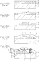
- FIG 13 illustrates a cross-sectional structure of a conventional semiconductor device.
- a lower electrode 2 made of a first platinum film, a capacitive insulating film 3 made of a ferroelectric film and an upper electrode 4 made of a second platinum film are formed in this order on a semiconductor substrate 1 made of silicon.
- the lower electrode 2 , the capacitive insulating film 3 and the upper electrode 4 constitute a capacitor device.
- An interlevel insulating film 5 made of a silicon oxide film, a silicon nitride film or the like is deposited to cover the entire surface of the semiconductor substrate 1 as well as the capacitor device.
- a lower-electrode contact hole 6 and an upper-electrode contact hole 7 are formed through the interlevel insulating film 5 .
- Metal interconnections 8 each consisting of a titanium film 8a , a first titanium nitride film 8b , an aluminum film 8c and a second titanium nitride film 8d , are formed to cover the interlevel insulating film 5 as well as the inner surfaces of the lower-electrode contact hole 6 and the upper-electrode contact hole 7 .
- the first platinum film 2A , the ferroelectric film 3A and the second platinum film 4A are sequentially stacked over the entire surface of the semiconductor substrate 1 . Thereafter, as shown in Figure 14(b) , the second platinum film 4A is selectively etched, thereby forming the upper electrode 4 . Then, in order to recover and stabilize the crystal structure of the ferroelectric film 3A , the ferroelectric film 3A is subjected to a heat treatment within oxygen ambient.
- the ferroelectric film 3A and the first platinum film 2A are selectively etched, thereby forming the capacitive insulating film 3 out of the ferroelectric film 3A and the lower electrode 2 out of the first platinum film 2A . Then, in order to recover and stabilize the crystal structure of the ferroelectric film constituting the capacitive insulating film 3 , the capacitive insulating film 3 is subjected to a heat treatment within oxygen ambient.
- the interlevel insulating film 5 made of a silicon oxide film or a silicon nitride film is deposited over the entire surface of the semiconductor substrate 1 . And the lower-electrode contact hole 6 and the upper-electrode contact hole 7 are formed through the interlevel insulating film 5 . Then, in order to recover and stabilize the crystal structure of the ferroelectric film constituting the capacitive insulating film 3 , the capacitive insulating film 3 is subjected to a heat treatment within oxygen ambient.
- the lower and the upper electrodes 2, 4 are made of platinum, which is hard to react with the ferroelectric film 3A constituting the capacitive insulating film 3 during the heat treatment and exhibits anti-oxidation properties even at a high temperature.
- the titanium film 8a , the first titanium nitride film 8b , the aluminum film 8c and the second titanium nitride film 8d are sequentially deposited to cover the entire surface of the semiconductor substrate 1 as well as the inner surfaces of the lower-electrode contact hole 6 and the upper-electrode contact hole 7 , thereby forming the metal interconnections 8 , each consisting of the titanium film 8a , the first titanium nitride film 8b , the aluminum film 8c and the second titanium nitride film 8d .
- the titanium film 8a functions as an adhesive film for improving the adhesion between the aluminum film 8c and the platinum film constituting the upper electrode 4 .
- the first titanium nitride film 8b functions as a barrier film for preventing aluminum in the aluminum film 8c from diffusing into the capacitive insulating film 3 .
- the second titanium nitride film 8d functions as an anti-reflection film while an upper interlevel insulating film deposited over the metal interconnections 8 is etched.
- the metal interconnections 8 are subjected to a heat treatment.
- the platinum film constituting the upper electrode comes to have column like crystal structure.
- the titanium atoms in the titanium film constituting the metal interconnections adversely pass through the grain boundary of the column like crystals of the platinum film constituting the upper electrode so as to diffuse into the capacitive insulating film.
- the composition of the ferroelectric film or the high dielectric film constituting the capacitive insulating film is varied, the electrical characteristics of the capacitor device are disadvantageously deteriorated.
- the upper electrode is made of platinum but also when the upper electrode is made of iridium, ruthenium, rhodium, palladium or the like that the upper electrode ordinarily has a column like crystal structure.
- the titanium atoms in the titanium film constituting the metal interconnections also adversely pass through the grain boundary of the column like crystals constituting the upper electrode so as to diffuse into the capacitive insulating film.
- the object of the present invention is to prevent titanium atoms in a titanium film from passing through the grain boundary of metal crystals composing the upper electrode of a capacitor device and diffusing into a capacitive insulating film during a heat treatment conducted on metal interconnections, which are formed on the capacitor device and include the titanium film.
- the semiconductor device includes: a substrate; a capacitor device, which is formed on the substrate and includes a capacitive lower electrode, a capacitive insulating film made of an insulating metal oxide film and a capacitive upper electrode; an interlevel insulating film, which is formed on the capacitor device and has an opening reaching the capacitive upper electrode; a metal interconnection, which is formed on the interlevel insulating film so as to be electrically connected to the capacitive upper electrode through the opening and includes a titanium film; and an anti-diffusion film, which is formed between the capacitive upper electrode and the metal interconnection, has conductivity and prevents titanium atoms composing the titanium film of the metal interconnection from passing through the capacitive upper electrode and diffusing into the capacitive insulating film.
- an anti-diffusion film for preventing titanium atoms composing the titanium film of the metal interconnection from passing through the capacitive upper electrode and diffusing into the capacitive insulating film is formed between the capacitive upper electrode and the metal interconnection.
- the titanium atoms in the titanium film do not pass through the grain boundary of metal crystals composing the capacitive upper electrode and do not diffuse into the capacitive insulating film. Accordingly, a semiconductor device including a highly reliable capacitor device can be formed.
- the anti-diffusion film is preferably a metal nitride film or metal oxide film having conductivity.
- the film can prevent the passage of titanium atoms with certainty.
- the anti-diffusion film is a conductive metal oxide film, the conductivity of the film is not damaged even when a heat treatment is conducted within oxygen ambient in order to recover the crystal structure of the ferroelectric film constituting the capacitive insulating film. This is because the metal oxide film has conductivity in the state of an oxide.
- the capacitive insulating film is a ferroelectric film, a highly reliable nonvolatile memory can be obtained.
- the capacitive insulating film is a high dielectric film, a highly reliable dynamic memory can be obtained.
- the titanium film is preferably an adhesive layer, formed as a lowermost layer of the metal interconnection, for improving adhesion between the metal interconnection and the upper electrode, and the anti-diffusion film is preferably a titanium nitride film.
- the titanium film is an adhesive layer, the adhesion between the metal interconnection and the upper electrode can be improved.
- the anti-diffusion film is a titanium nitride film, then no by-product is formed during the deposition of the anti-diffusion film.
- titanium in the titanium film diffuses toward the anti-diffusion film over a certain distance, the nature of the anti-diffusion film is not changed and the characteristics of the capacitor device are stabilized.
- the capacitive upper electrode preferably has a crystal structure including a grain boundary.
- the titanium atoms are more likely to pass through the capacitive upper electrode, the titanium atoms do not diffuse into the capacitive insulating film because the atoms are prevented by the anti-diffusion film from reaching the capacitive upper electrode.
- a first method for fabricating a semiconductor device includes the steps of: forming a capacitor device, including a capacitive lower electrode, a capacitive insulating film made of an insulating metal oxide film and a capacitive upper electrode, on a substrate; forming an interlevel insulating film, having a contact hole reaching the capacitive upper electrode, on the capacitor device; depositing a conductive film, preventing the passage of titanium atoms therethrough, so as to cover the entire surface of the interlevel insulating film as well as the contact hole; patterning the conductive film such that at least a part of the conductive film located inside the contact hole is left, thereby forming an anti-diffusion film out of the conductive film; and forming, on the interlevel insulating film, a metal interconnection including a titanium film such that the metal interconnection is electrically connected to the capacitive upper electrode via the anti-diffusion film.
- a conductive film preventing the passage of titanium atoms, is deposited over an interlevel insulating film formed on the capacitor device and including a contact hole. Then, the conductive film is patterned, thereby leaving the part of the conductive film located inside the contact hole.
- the anti-diffusion film for preventing the titanium atoms from passing through the capacitive upper electrode and diffusing into the capacitive insulating film can be formed between the upper electrode of the capacitor device and the metal interconnection with certainty.
- a second method for fabricating a semiconductor device includes the steps of: forming a capacitor device, including a capacitive lower electrode, a capacitive insulating film made of an insulating metal oxide film and a capacitive upper electrode, on a substrate; forming an interlevel insulating film, having a contact hole reaching the capacitive upper electrode, on the capacitor device; forming, on the interlevel insulating film, a resist pattern having an opening at a site corresponding to the contact hole; depositing a conductive film, preventing the passage of titanium atoms therethrough, so as to cover the entire surface of the resist pattern; lifting off the conductive film together with the resist pattern such that a part of the conductive film located inside the contact hole is left, thereby forming an anti-diffusion film out of the conductive film; and forming, on the interlevel insulating film, a metal interconnection including a titanium film such that the metal interconnection is electrically connected to the capacitive upper electrode via the anti-diffusion film.
- a resist pattern having an opening at a site corresponding to a contact hole is formed on the interlevel insulating film formed on the capacitor device and including the contact hole, and a conductive film, preventing the passage of titanium atoms therethrough, is deposited thereon.
- the anti-diffusion film for preventing the titanium atoms from passing through the capacitive upper electrode and diffusing into the capacitive insulating film can be formed between the upper electrode of the capacitor device and the metal interconnection with certainty.
- a third method for fabricating a semiconductor device includes the steps of: sequentially stacking a first metal film, an insulating metal oxide film, a second metal film and a conductive film, preventing the passage of titanium atoms therethrough, on a substrate; patterning the second metal film and the conductive film by using the same etching mask, thereby forming a capacitive upper electrode out of the second metal film and an anti-diffusion film out of the conductive film; patterning the insulating metal oxide film to form a capacitive insulating film and patterning the first metal film to form a capacitive lower electrode; forming an interlevel insulating film, having a contact hole reaching the capacitive upper electrode, over a capacitor device constituted by the capacitive lower electrode, the capacitive insulating film and the capacitive upper electrode; and forming, on the interlevel insulating film, a metal interconnection including a titanium film such that the metal interconnection is electrically connected to the capacitive upper electrode via the anti-d
- the second metal film and the conductive film are patterned first, thereby forming a capacitive upper electrode and an anti-diffusion film. Then, a metal interconnection including a titanium film is formed over the interlevel insulating film having a contact hole.
- the anti-diffusion film for preventing the titanium atoms from passing through the capacitive upper electrode and diffusing into the capacitive insulating film can be formed between the upper electrode of the capacitor device and the metal interconnection with certainty.
- a fourth method for fabricating a semiconductor device includes the steps of: forming a capacitive lower electrode and a capacitive insulating film made of an insulating metal oxide film on a substrate; depositing an interlevel insulating film so as to cover the substrate as well as the capacitive insulating film; forming a resist pattern over the interlevel insulating film, the resist pattern having an opening over a region where a capacitive upper electrode is to be formed; etching the interlevel insulating film by using the resist pattern as a mask, thereby forming an upper electrode forming opening through the interlevel insulating film; sequentially depositing a metal film and a conductive film preventing the passage of titanium atoms therethrough so as to cover the entire surface of the resist pattern as well as the upper electrode forming opening; lifting off the metal film and the conductive film together with the resist pattern such that part of the metal film and part of the conductive film, which are located in the upper electrode forming opening, are left, thereby forming the capacitive
- the interlevel insulating film is etched by using, as a mask, a resist pattern including an opening over the region where the capacitive upper electrode is to be formed, thereby forming an upper electrode forming opening through the interlevel insulating film. Then, a metal film and a conductive film preventing the passage of titanium atoms therethrough are deposited, and a metal interconnection including a titanium film is formed thereon.
- the anti-diffusion film for preventing the titanium atoms from passing through the capacitive upper electrode and diffusing into the capacitive insulating film can be formed between the upper electrode of the capacitor device and the metal interconnection with certainty.
- the semiconductor device of the present invention can be fabricated with certainty.
- the conductive film is preferably a metal nitride film or metal oxide film having conductivity.
- the capacitive insulating film is preferably a ferroelectric film or a high dielectric film.
- the titanium film is preferably an adhesive layer, formed as a lowermost layer of the metal interconnection, for improving adhesion between the metal interconnection and the capacitive upper electrode, and the anti-diffusion film is preferably a titanium nitride film.
- the capacitive upper electrode preferably has a crystal structure including a grain boundary.
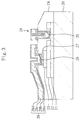
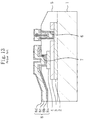
- Figure 1 illustrates a cross-sectional structure of the semiconductor device in the first embodiment.
- a lower electrode 11 made of a first platinum film
- a capacitive insulating film 12 made of an insulating metal oxide film such as a ferroelectric film or a high dielectric film
- an upper electrode 13 made of a second platinum film
- the lower electrode 11 , the capacitive insulating film 12 and the upper electrode 13 constitute a capacitor device.
- the size of the lower electrode 11 is larger than that of the upper electrode 13 such that a metal interconnection can be extended upward to pass by the sides of the upper electrode 13 and be electrically connected to the lower electrode 11 .
- a lower-electrode contact hole 15 and an upper-electrode contact hole 16 are formed through the interlevel insulating film 14 .
- the first embodiment is characterized by including an anti-diffusion conductive film 17 made of a conductive metal nitride film (e.g., a titanium nitride film) on the inner bottom surface and inner wall surfaces of the upper-electrode contact hole 16 and on a part of the interlevel insulating film 14 surrounding the upper-electrode contact hole 16 .
- a conductive metal nitride film e.g., a titanium nitride film
- Metal interconnections 18 are formed over the interlevel insulating film 14 as well as the inner surfaces of the lower-electrode contact hole 15 and the upper-electrode contact hole 16 .
- one of the metal interconnections 18 is electrically connected to the lower electrode 11 directly inside the lower-electrode contact hole 15 .
- the other metal interconnection 18 is electrically connected to the upper electrode 13 via the anti-diffusion conductive film 17 inside the upper-electrode contact hole 16 .
- the titanium film 18a functions as an adhesive layer for improving the adhesion between the aluminum film 18c and the lower electrode 11 and between the aluminum film 18c and the upper electrode 13 .
- the first titanium nitride film 18b functions as a barrier layer for preventing aluminum in the aluminum film 18c from diffusing into the capacitive insulating film 12 .
- the second titanium nitride film 18d functions as an anti-reflection film while an upper interlevel insulating film to be deposited on the metal interconnections 18 is etched.
- the first platinum film 11A , the ferroelectric film 12A and the second platinum film 13A are sequentially stacked over the entire surface of the semiconductor substrate 10 .
- the second platinum film 13A is selectively etched, thereby forming the upper electrode 13 .
- the ferroelectric film 12A and the first platinum film 11A are selectively etched, thereby forming the capacitive insulating film 12 out of the ferroelectric film 12A and the lower electrode 11 out of the first platinum film 11A .
- the ferroelectric film 12A and the first platinum film 11A are preferably etched by using the same mask, because mask misalignment can be prevented by doing so.
- the ferroelectric film 12A and the first platinum film 11A may be etched separately by using respectively different masks.
- the capacitive insulating film 12 is selectively etched in order to form a region from which a metal interconnection to be electrically connected to the lower electrode 11 is extended upward. Subsequently, in order to recover and stabilize the crystal structure of the ferroelectric film constituting the capacitive insulating film 12 , the capacitive insulating film 12 is subjected to a heat treatment within oxygen ambient.
- the interlevel insulating film 14 made of a silicon oxide film is deposited over the entire surface of the semiconductor substrate 10 . And the interlevel insulating film 14 is selectively etched, thereby forming the lower-electrode contact hole 15 and the upper-electrode contact hole 16 . Then, in order to recover and stabilize the crystal structure of the ferroelectric film constituting the capacitive insulating film 12 , the capacitive insulating film 12 is subjected to a heat treatment within oxygen ambient.
- the titanium nitride film 17A is deposited so as to cover the entire surface of the semiconductor substrate 10 as well as the inner surfaces of the lower-electrode contact hole 15 and the upper-electrode contact hole 16 . Then, a resist pattern 19 having an opening over the upper-electrode contact hole 16 and the surrounding region thereof is formed over the titanium nitride film 17A .
- the titanium nitride film 17A is etched by using the resist pattern 19 as a mask, thereby forming the anti-diffusion conductive film 17 out of the titanium nitride film 17A so as to cover the inner bottom surface and inner wall surfaces of the upper-electrode contact hole 16 and part of the upper surface of the interlevel insulating film 14 surrounding the upper-electrode contact hole 16 .
- the metal interconnections 18 are formed over the anti-diffusion conductive film 17 and the interlevel insulating film 14 .
- the titanium film 18a functions as an adhesive layer for improving the adhesion between the aluminum film 18c and the lower electrode 11 and between the aluminum film 18c and the upper electrode 13 .
- the first titanium nitride film 18b functions as a barrier layer for preventing aluminum in the aluminum film 18c from diffusing into the capacitive insulating film 12.
- the second titanium nitride film 18d functions as an anti-reflection film while an upper interlevel insulating film to be deposited over the metal interconnections 18 is etched.
- the metal interconnections 18 are subjected to a heat treatment.
- the inner bottom surface and inner wall surfaces of the upper-electrode contact hole 16 and the part of the upper surface of the interlevel insulating film 14 surrounding the upper-electrode contact hole 16 are covered with the anti-diffusion conductive film 17 made of the titanium nitride film 17A including no grain boundaries and having a dense structure.
- the titanium atoms in the titanium film 18a constituting the metal interconnections 18 do not pass through the anti-diffusion conductive film 17 . Accordingly, during the heat treatment conducted on the metal interconnections 18 , it is possible to prevent the titanium atoms in the titanium film 18a from passing through the grain boundaries of metal crystals composing the upper electrode 13 and diffusing into the capacitive insulating film 12 .
- a semiconductor device including a highly reliable capacitor device can be formed.
- the inner surfaces of the upper-electrode contact hole 16 but also the part of the upper surface of the interlevel insulating film 14 surrounding the upper-electrode contact hole 16 are covered with the anti-diffusion conductive film 17 .
- the inner bottom surface of the upper-electrode contact hole 16 can be covered with the anti-diffusion conductive film 17 with certainty.
- Table 1 shows in comparison the characteristics of the capacitor device in the semiconductor device of the first embodiment and the characteristics of a capacitor device in a conventional semiconductor device.
- the breakdown voltage of the capacitor device is 40 V, which is twice as high as that of the conventional capacitor device.
- the data retention time of the capacitor device of the first embodiment is 10 years, which is ten times as long as that of the conventional capacitor device.
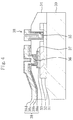
- FIG. 2 illustrates a cross-sectional structure of the semiconductor device in the second embodiment.
- a lower electrode 21 made of a first platinum film a capacitive insulating film 22 made of an insulating metal oxide film such as a ferroelectric film or a high dielectric film, and an upper electrode 23 made of a second platinum film are sequentially formed on a semiconductor substrate 20 made of silicon.
- the lower electrode 21 , the capacitive insulating film 22 and the upper electrode 23 constitute a capacitor device.
- a lower-electrode contact hole 25 and an upper-electrode contact hole 26 are formed through the interlevel insulating film 24 .
- the second embodiment is characterized in that an anti-diffusion conductive film 27 made of a titanium nitride film is filled in the upper-electrode contact hole 26 .
- Metal interconnections 28 are formed so as to cover the interlevel insulating film 24 as well as the inner surfaces of the lower-electrode contact hole 25 .
- one of the metal interconnections 28 is electrically connected to the lower electrode 21 directly inside the lower-electrode contact hole 25 .
- the other metal interconnection 28 is electrically connected to the upper electrode 23 via the anti-diffusion conductive film 27 above the upper-electrode contact hole 26 .
- the latter metal interconnection 28 is electrically connected to the upper electrode 23 without being bent in the vertical direction.
- the latter metal interconnection 28 can be electrically connected to the upper electrode 23 with more certainty.
- Figure 3 illustrates a cross-sectional structure of the semiconductor device in the variation of the second embodiment. Only the difference between the second embodiment and this variation will be described below.
- the variation of the second embodiment is characterized in that the anti-diffusion conductive film 27 made of a titanium nitride film, for example, is deposited only in the lower part inside the upper-electrode contact hole 26 .
- part of the metal interconnection 28 consisting of the titanium film 28a , the first titanium nitride film 28b , the aluminum film 28c and the second titanium nitride film 28d is located inside the upper-electrode contact hole 26 .
- one of the metal interconnections 28 is electrically connected to the lower electrode 21 directly inside the lower-electrode contact hole 25 .
- the other metal interconnection 28 is electrically connected to the upper electrode 23 via the anti-diffusion conductive film 27 inside the upper-electrode contact hole 26 .
- the first platinum film 21A , the ferroelectric film 22A and the second platinum film 23A are sequentially stacked over the entire surface of the semiconductor substrate 20 .
- the second platinum film 23A is selectively etched, thereby forming the upper electrode 23 .
- the ferroelectric film 22A and the first platinum film 21A are selectively etched, thereby forming the capacitive insulating film 22 out of the ferroelectric film 22A and the lower electrode 21 out of the first platinum film 21A .
- the capacitive insulating film 22 is selectively etched in order to form a region from which a metal interconnection to be electrically connected to the lower electrode 21 is extended upward.
- the capacitive insulating film 22 is subjected to a heat treatment within oxygen ambient.
- the interlevel insulating film 24 made of a silicon oxide film is deposited over the entire surface of the semiconductor substrate 20 . And the interlevel insulating film 24 is selectively etched, thereby forming the lower-electrode contact hole 25 and the upper-electrode contact hole 26 . Then, in order to recover and stabilize the crystal structure of the ferroelectric film constituting the capacitive insulating film 22 , the capacitive insulating film 22 is subjected to a heat treatment within oxygen ambient.
- a resist pattern 29 having an opening in a region corresponding to the upper-electrode contact hole 26 is formed over the interlevel insulating film 24 and the titanium nitride film 27A is deposited over the entire surface of the semiconductor substrate 20 .
- the resist pattern 29 is removed and the titanium nitride film 27A deposited on the resist pattern 29 is lifted off, thereby forming the anti-diffusion conductive film 27 out of the titanium nitride film 27A so as to fill in only the inside of the upper-electrode contact hole 26 .
- the metal interconnections 28 are formed over the anti-diffusion conductive film 27 and the interlevel insulating film 24 .
- the metal interconnections 28 are subjected to a heat treatment.
- the anti-diffusion conductive film 27 made of the titanium nitride film 27A including no grain boundaries and having a dense structure is formed inside the upper-electrode contact hole 26 .
- the titanium atoms in the titanium film 28a constituting the metal interconnections 28 do not pass through the anti-diffusion conductive film 27 .
- a semiconductor device including a highly reliable capacitor device can be formed.
- the metal interconnection 28 is not bent over the upper-electrode contact hole 26 .
- the contact between the metal interconnection 28 and the upper electrode 23 is satisfactory.
- Table 2 shows in comparison the characteristics of the capacitor device in the semiconductor device of the second embodiment and the characteristics of a capacitor device in a conventional semiconductor device.
- the breakdown voltage of the capacitor device is 40 V, which is twice as high as that of the conventional capacitor device.
- the data retention time of the capacitor device of the second embodiment is 10 years, which is ten times as long as that of the conventional capacitor device.
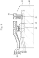
- FIG 4 illustrates a cross-sectional structure of the semiconductor device in the third embodiment.
- a lower electrode 31 made of a first platinum film, a capacitive insulating film 32 made of an insulating metal oxide film such as a ferroelectric film or a high dielectric film, and an upper electrode 33 made of a second platinum film are sequentially formed on a semiconductor substrate 30 made of silicon.
- the lower electrode 31 , the capacitive insulating film 32 and the upper electrode 33 constitute a capacitor device.
- a lower-electrode contact hole 35 and an upper-electrode contact hole 36 are formed through the interlevel insulating film 34 .
- the third embodiment is characterized in that an anti-diffusion conductive film 37 made of a titanium nitride film having the same planar shape as that of the upper electrode 33 is formed on the upper electrode 33 .
- Metal interconnections 38 are formed to cover the interlevel insulating film 34 as well as the inner surfaces of the lower-electrode contact hole 35 and the upper-electrode contact hole 36 .
- one of the metal interconnections 38 is electrically connected to the lower electrode 31 directly inside the lower-electrode contact hole 35 .
- the other metal interconnection 38 is electrically connected to the upper electrode 33 at the bottom of the upper-electrode contact hole 36 via the anti-diffusion conductive film 37 .
- the first platinum film 31A , the ferroelectric film 32A , the second platinum film 33A and the titanium nitride film 37A are sequentially stacked over the entire surface of the semiconductor substrate 30 .
- the titanium nitride film 37A and the second platinum film 33A are patterned by using the same etching mask, thereby forming the anti-diffusion conductive film 37 out of the titanium nitride film 37A and the upper electrode 33 out of the second platinum film 33A .
- the ferroelectric film 32A is subjected to a heat treatment within oxygen ambient.
- the ferroelectric film 32A and the first platinum film 31A are patterned, thereby forming the capacitive insulating film 32 out of the ferroelectric film 32A and the lower electrode 31 out of the first platinum film 31A .
- the capacitive insulating film 32 is selectively etched in order to form a region from which a metal interconnection to be electrically connected to the lower electrode 31 is extended upward.
- the capacitive insulating film 32 is subjected to a heat treatment within oxygen ambient.
- the interlevel insulating film 34 made of a silicon oxide film is deposited over the entire surface of the semiconductor substrate 30 . And the interlevel insulating film 34 is selectively etched, thereby forming the lower-electrode contact hole 35 and the upper-electrode contact hole 36 . Then, in order to recover and stabilize the crystal structure of the ferroelectric film constituting the capacitive insulating film 32 , the capacitive insulating film 32 is subjected to a heat treatment within oxygen ambient.
- the metal interconnections 38 are formed over the anti-diffusion conductive film 37 and the interlevel insulating film 34 . Then, in order to further improve the adhesion between the titanium film 38a constituting the metal interconnections 38 and the interlevel insulating film 34 , the metal interconnections 38 are subjected to a heat treatment.
- the anti-diffusion conductive film 37 made of the titanium nitride film 37A including no grain boundaries and having a dense structure is formed under the bottom of the upper-electrode contact hole 36 .
- the titanium atoms in the titanium film 38a constituting the metal interconnection 38 do not pass through the anti-diffusion conductive film 37 .
- a semiconductor device including a highly reliable capacitor device can be formed.
- Table 3 shows in comparison the characteristics of the capacitor device in the semiconductor device of the third embodiment and the characteristics of a capacitor device in a conventional semiconductor device.
- the breakdown voltage of the capacitor device is 40 V, which is twice as high as that of the conventional capacitor device.
- the data retention time of the capacitor device of the third embodiment is 10 years, which is ten times as long as that of the conventional capacitor device.
- FIG. 5 illustrates a cross-sectional structure of the semiconductor device in the fourth embodiment.
- a lower electrode 41 made of a first platinum film a capacitive insulating film 42 made of an insulating metal oxide film such as a ferroelectric film or a high dielectric film, and an upper electrode 43 made of a second platinum film are sequentially formed on a semiconductor substrate 40 made of silicon.
- the lower electrode 41 , the capacitive insulating film 42 and the upper electrode 43 constitute a capacitor device.
- An interlevel insulating film 44 made of a silicon oxide film, a silicon nitride film or the like, is deposited to cover the entire surface of the semiconductor substrate 40 as well as the capacitor device.
- a lower-electrode contact hole 45 and an upper-electrode contact hole 46 are formed through the interlevel insulating film 44 .
- the fourth embodiment is characterized in that an anti-diffusion conductive film 47 made of a titanium nitride film, for example, is deposited so as to fill in only the lower part inside the lower-electrode contact hole 45 and the lower part inside the upper-electrode contact hole 46 .
- Metal interconnections 48 each consisting of a titanium film 48a , a first titanium nitride film 48b , an aluminum film 48c and a second titanium nitride film 48d , are formed to cover the interlevel insulating film 44 as well as the inner surfaces of the lower-electrode contact hole 45 and the upper-electrode contact hole 46 .
- one of the metal interconnections 48 is electrically connected to the lower electrode 41 via the anti-diffusion conductive film 47 inside the lower-electrode contact hole 45 .
- the other metal interconnection 48 is electrically connected to the upper electrode 43 via the anti-diffusion conductive film 47 inside the upper-electrode contact hole 46 .
- the first platinum film 41A and the ferroelectric film 42A are sequentially stacked over the entire surface of the semiconductor substrate 40 .
- the ferroelectric film 42A and the first platinum film 41A are selectively etched, thereby forming the capacitive insulating film 42 out of the ferroelectric film 42A and the lower electrode 41 out of the first platinum film 41A .
- the capacitive insulating film 42 is selectively etched in order to form a region from which a metal interconnection to be electrically connected to the lower electrode 41 is extended upward.
- the capacitive insulating film 42 is subjected to a heat treatment within oxygen ambient.
- the interlevel insulating film 44 is deposited over the entire surface of the semiconductor substrate 40 .
- a resist pattern 49 having openings over the respective regions where the lower-electrode contact hole and the upper-electrode contact hole are to be formed, is formed over the interlevel insulating film 44 .
- the interlevel insulating film 44 is patterned by using the resist pattern 49 as an etching mask, thereby forming the lower-electrode contact hole 45 and the upper-electrode contact hole 46 through the interlevel insulating film 44 .
- the second platinum film 43A and the titanium nitride film 47A are sequentially deposited to cover the entire surface including the inner surfaces of the lower-electrode contact hole 45 and the upper-electrode contact hole 46 .
- the resist pattern 49 is removed and the second platinum film 43A and the titanium nitride film 47A deposited on the resist pattern 49 are lifted off, thereby leaving the second platinum film 43A inside the lower-electrode contact hole 45 and forming the anti-diffusion conductive film 47 out of the titanium nitride film 47A thereon. Also, inside the upper-electrode contact hole 46 , the upper electrode 43 is formed out of the second platinum film 43A and the anti-diffusion conductive film 47 is formed out of the titanium nitride film 47A .
- the metal interconnections 48 are formed over the anti-diffusion conductive film 47 and the interlevel insulating film 44 .
- the metal interconnections 48 are subjected to a heat treatment.
- the anti-diffusion conductive film 47 made of the titanium nitride film 47A including no grain boundaries and having a dense structure is formed inside the upper-electrode contact hole 46 .
- the titanium atoms in the titanium film 48a constituting the metal interconnections 48 do not pass through the anti-diffusion conductive film 47 . Accordingly, during the heat treatment conducted on the metal interconnections 48 , it is possible to prevent the titanium atoms in the titanium film 48a from passing through the grain boundaries of metal crystals composing the upper electrode 43 and diffusing into the capacitive insulating film 42 .
- a semiconductor device including a highly reliable capacitor device can be formed.
- Table 4 shows in comparison the characteristics of the capacitor device in the semiconductor device of the fourth embodiment and the characteristics of a capacitor device in a conventional semiconductor device.
- the breakdown voltage of the capacitor device is 40 V, which is twice as high as that of the conventional capacitor device.
- the data retention time of the capacitor device of the fourth embodiment is 10 years, which is ten times as long as that of the conventional capacitor device.
- a titanium nitride film is used as the anti-diffusion conductive film 17, 27, 37, 47 .
- metal films, metal nitride films and metal oxide films include no grain boundaries and have a dense structure, these films also prevent the passage of titanium atoms in the titanium film composing the metal interconnections 18, 28, 38, 48, in the same way as the titanium nitride film.
- the conductivity of the metal oxide film is not damaged even when a heat treatment is conducted within oxygen ambient in order to recover and stabilize the crystal structure of the ferroelectric film constituting the capacitive insulating film 12, 22, 32, 42. This is because the metal oxide film has conductivity in the state of an oxide.
- a multi-layer structure including at least two types of films selected from the metal films, the metal nitride films and the metal oxide films may be used as the anti-diffusion conductive film 17, 27, 37, 47.
- a multi-layer film including a platinum film and an iridium oxide film instead of the platinum film, may be used as the lower electrode 11, 21, 31, 41 and/or the upper electrode 13, 23, 33, 43.
- a plurality of upper electrodes 33, 43 and a plurality of anti-diffusion conductive films 37, 47 may be alternately stacked.
- a stable upper electrode which is very less likely to be deformed because of thermal expansion, can be formed.
- a perovskite ferroelectric film made of barium titanate, lead titanate zirconate or the like, or a bismuth layer shaped perovskite ferroelectric film made of SrBi 2 Ta 2 O 9 or the like may be used as the ferroelectric film constituting the capacitive insulating film 12, 22, 32, 42 .
- the capacitor device may be applied to a dynamic RAM.
- a silicon nitride film or a silicon oxynitride film instead of the silicon oxide film, may be used as the interlevel insulating film 14, 24, 34, 44 .
- the semiconductor substrate 10, 20, 30, 40 may be an insulating substrate (such as a glass substrate), a conductive substrate or a semiconductor substrate on which transistors or the like are formed.
Abstract
Description


Claims (13)
- A semiconductor device comprising:a substrate;a capacitor device, which is formed on the substrate and includes a capacitive lower electrode, a capacitive insulating film made of an insulating metal oxide film and a capacitive upper electrode;an interlevel insulating film, which is formed over the capacitor device and has an opening reaching the capacitive upper electrode;a metal interconnection, which is formed on the interlevel insulating film so as to be electrically connected to the capacitive upper electrode through the opening and includes a titanium film; andan anti-diffusion film, which is formed between the capacitive upper electrode and the metal interconnection, has conductivity and prevents titanium atoms, composing the titanium film of the metal interconnection, from passing through the capacitive upper electrode and diffusing into the capacitive insulating film.
- The semiconductor device of Claim 1, characterized in that the anti-diffusion film is a metal nitride film or metal oxide film having conductivity.
- The semiconductor device of Claim 1, characterized in that the capacitive insulating film is a ferroelectric film or a high dielectric film.
- The semiconductor device of Claim 1, characterized in that the titanium film is an adhesive layer, formed as a lowermost layer of the metal interconnection, for improving adhesion between the metal interconnection and the upper electrode,
and wherein the anti-diffusion film is a titanium nitride film. - The semiconductor device of Claim 1, characterized in that the capacitive upper electrode has a crystal structure including a grain boundary.
- A method for fabricating a semiconductor device, comprising the steps of:forming a capacitor device including a capacitive lower electrode, a capacitive insulating film made of an insulating metal oxide film and a capacitive upper electrode on a substrate;forming an interlevel insulating film, having a contact hole reaching the capacitive upper electrode, over the capacitor device;depositing a conductive film preventing the passage of titanium atoms therethrough so as to cover the entire surface of the interlevel insulating film as well as the contact hole;patterning the conductive film such that at least a part of the conductive film located inside the contact hole is left, thereby forming an anti-diffusion film out of the conductive film; andforming, on the interlevel insulating film, a metal interconnection including a titanium film such that the metal interconnection is electrically connected to the capacitive upper electrode via the anti-diffusion film.
- A method for fabricating a semiconductor device, comprising the steps of:forming a capacitor device including a capacitive lower electrode, a capacitive insulating film made of an insulating metal oxide film and a capacitive upper electrode on a substrate;forming an interlevel insulating film, having a contact hole reaching the capacitive upper electrode, on the capacitor device;forming, on the interlevel insulating film, a resist pattern having an opening at a site corresponding to the contact hole;depositing a conductive film preventing the passage of titanium atoms therethrough so as to cover the entire surface of the resist pattern;lifting off the conductive film together with the resist pattern such that a part of the conductive film located inside the contact hole is left, thereby forming an anti-diffusion film out of the conductive film; andforming, on the interlevel insulating film, a metal interconnection including a titanium film such that the metal interconnection is electrically connected to the capacitive upper electrode via the anti-diffusion film.
- A method for fabricating a semiconductor device, comprising the steps of:sequentially stacking a first metal film, an insulating metal oxide film, a second metal film and a conductive film, which prevents the passage of titanium atoms therethrough, on a substrate;patterning the second metal film and the conductive film by using the same etching mask, thereby forming a capacitive upper electrode out of the second metal film and an anti-diffusion film out of the conductive film;patterning the insulating metal oxide film to form a capacitive insulating film and patterning the first metal film to form a capacitive lower electrode;forming an interlevel insulating film, having a contact hole reaching the capacitive upper electrode, over a capacitor device constituted by the capacitive lower electrode, the capacitive insulating film and the capacitive upper electrode; andforming, on the interlevel insulating film, a metal interconnection including a titanium film such that the metal interconnection is electrically connected to the capacitive upper electrode via the anti-diffusion film.
- A method for fabricating a semiconductor device, comprising the steps of:forming a capacitive lower electrode and a capacitive insulating film made of an insulating metal oxide film on a substrate;depositing an interlevel insulating film so as to cover the substrate as well as the capacitive insulating film;forming a resist pattern over the interlevel insulating film, the resist pattern having an opening over a region where a capacitive upper electrode is to be formed;etching the interlevel insulating film by using the resist pattern as a mask, thereby forming an upper electrode forming opening through the interlevel insulating film;sequentially depositing a metal film and a conductive film preventing the passage of titanium atoms therethrough so as to cover the entire surface of the resist pattern as well as the upper electrode forming opening;lifting off the metal film and the conductive film together with the resist pattern such that part of the metal film and part of the conductive film, which are located in the upper electrode forming opening, are left, thereby forming the capacitive upper electrode out of the metal film and an anti-diffusion film out of the conductive film; andforming, on the interlevel insulating film, a metal interconnection including a titanium film such that the metal interconnection is electrically connected to the capacitive upper electrode via the anti-diffusion film.
- The method for fabricating a semiconductor device of Claims 6 to 9, characterized in that the conductive film is a metal nitride film or metal oxide film having conductivity.
- The method for fabricating a semiconductor device of Claims 6 to 9, characterized in that the capacitive insulating film is a ferroelectric film or a high dielectric film.
- The method for fabricating a semiconductor device of Claims 6 to 9, characterized in that the titanium film is an adhesive layer, formed as a lowermost layer of the metal interconnection, for improving adhesion between the metal interconnection and the capacitive upper electrode,
and wherein the anti-diffusion film is a titanium nitride film. - The method for fabricating a semiconductor device of Claims 6 to 9, wherein the capacitive upper electrode has a crystal structure including a grain boundary.
Applications Claiming Priority (6)
| Application Number | Priority Date | Filing Date | Title |
|---|---|---|---|
| JP198118/97 | 1997-07-24 | ||
| JP19811997 | 1997-07-24 | ||
| JP19811897 | 1997-07-24 | ||
| JP19811997 | 1997-07-24 | ||
| JP19811897 | 1997-07-24 | ||
| JP198119/97 | 1997-07-24 |
Publications (2)
| Publication Number | Publication Date |
|---|---|
| EP0893832A2 true EP0893832A2 (en) | 1999-01-27 |
| EP0893832A3 EP0893832A3 (en) | 1999-11-03 |
Family
ID=26510773
Family Applications (1)
| Application Number | Title | Priority Date | Filing Date |
|---|---|---|---|
| EP98113701A Withdrawn EP0893832A3 (en) | 1997-07-24 | 1998-07-22 | Semiconductor device including a capacitor device and method for fabricating the same |
Country Status (6)
| Country | Link |
|---|---|
| US (3) | US6239462B1 (en) |
| EP (1) | EP0893832A3 (en) |
| KR (1) | KR100568385B1 (en) |
| CN (1) | CN1173403C (en) |
| SG (1) | SG74643A1 (en) |
| TW (1) | TW395037B (en) |
Families Citing this family (20)
| Publication number | Priority date | Publication date | Assignee | Title |
|---|---|---|---|---|
| US6052271A (en) * | 1994-01-13 | 2000-04-18 | Rohm Co., Ltd. | Ferroelectric capacitor including an iridium oxide layer in the lower electrode |
| JP3517876B2 (en) * | 1998-10-14 | 2004-04-12 | セイコーエプソン株式会社 | Ferroelectric thin film element manufacturing method, ink jet recording head, and ink jet printer |
| JP3217326B2 (en) * | 1999-03-19 | 2001-10-09 | 富士通株式会社 | Ferroelectric memory with electromagnetic shielding structure |
| KR100349642B1 (en) * | 1999-06-28 | 2002-08-22 | 주식회사 하이닉스반도체 | Ferroelectric random access memory device and method for forming the same |
| KR100305680B1 (en) * | 1999-08-26 | 2001-11-01 | 윤종용 | method for fabricating capacitor of semiconductor integrated circuit |
| KR100604662B1 (en) * | 2000-06-30 | 2006-07-25 | 주식회사 하이닉스반도체 | Semiconductor device capable of improving adhesion characteristic between upper electrode and interlayer insulating layer and method for forming the same |
| KR100599432B1 (en) * | 2000-06-30 | 2006-07-14 | 주식회사 하이닉스반도체 | Method for forming metal wire of FeRAM |
| JP4008651B2 (en) * | 2000-10-31 | 2007-11-14 | 株式会社東芝 | Semiconductor device and manufacturing method thereof |
| US6750113B2 (en) * | 2001-01-17 | 2004-06-15 | International Business Machines Corporation | Metal-insulator-metal capacitor in copper |
| US6613641B1 (en) * | 2001-01-17 | 2003-09-02 | International Business Machines Corporation | Production of metal insulator metal (MIM) structures using anodizing process |
| US20020138417A1 (en) * | 2001-03-20 | 2002-09-26 | David Lawrence | Risk management clearinghouse |
| JP2003152165A (en) * | 2001-11-15 | 2003-05-23 | Fujitsu Ltd | Semiconductor device and manufacturing method thereof |
| KR100533971B1 (en) * | 2002-12-12 | 2005-12-07 | 주식회사 하이닉스반도체 | Method of manufacturing capacitor for semiconductor device |
| JP4049119B2 (en) * | 2004-03-26 | 2008-02-20 | セイコーエプソン株式会社 | Method for manufacturing ferroelectric memory device |
| US20070075348A1 (en) * | 2005-09-30 | 2007-04-05 | Texas Instrument Incorporated | High density, high Q capacitor on top of a protective layer |
| US20080137262A1 (en) * | 2006-12-12 | 2008-06-12 | Texas Instruments Inc. | Methods and systems for capacitors |
| US8395196B2 (en) | 2010-11-16 | 2013-03-12 | International Business Machines Corporation | Hydrogen barrier liner for ferro-electric random access memory (FRAM) chip |
| TWI536607B (en) * | 2013-11-11 | 2016-06-01 | 隆達電子股份有限公司 | An electrode structure |
| CN109216360B (en) | 2017-07-07 | 2021-01-12 | 联华电子股份有限公司 | Semiconductor memory device with a plurality of memory cells |
| US11532698B2 (en) * | 2019-09-11 | 2022-12-20 | Taiwan Semiconductor Manufacturing Company, Ltd. | Diffusion barrier layer in top electrode to increase break down voltage |
Citations (8)
| Publication number | Priority date | Publication date | Assignee | Title |
|---|---|---|---|---|
| EP0404295A1 (en) * | 1989-06-20 | 1990-12-27 | Ramtron International Corporation | Method for fabricatinf integrated circuit capacitors |
| EP0448151A1 (en) * | 1990-03-16 | 1991-09-25 | Koninklijke Philips Electronics N.V. | Method of manufacturing a semiconductor device comprising capacitors which form memory elements and comprise a ferroelectric dielectric material |
| EP0557937A1 (en) * | 1992-02-25 | 1993-09-01 | Ramtron International Corporation | Ozone gas processing for ferroelectric memory circuits |
| EP0574275A1 (en) * | 1992-06-12 | 1993-12-15 | Matsushita Electronics Corporation | Semiconductor device having capacitor and manufacturing method thereof |
| US5475248A (en) * | 1990-09-28 | 1995-12-12 | Ramtron International Corporation | Semiconductor device with a conductive reaction-preventing film |
| US5581436A (en) * | 1994-08-01 | 1996-12-03 | Texas Instruments Incorporated | High-dielectric-constant material electrodes comprising thin platinum layers |
| DE19636054A1 (en) * | 1995-09-08 | 1997-03-13 | Toshiba Kawasaki Kk | Semiconductor device, e.g. DRAM |
| EP0766319A2 (en) * | 1995-09-29 | 1997-04-02 | Sony Corporation | Capacitor having ferroelectric film for nonvolatile memory cell, and method of manufacturing the same |
Family Cites Families (21)
| Publication number | Priority date | Publication date | Assignee | Title |
|---|---|---|---|---|
| DE69213094T2 (en) | 1991-05-08 | 1997-03-06 | Philips Electronics Nv | Method for producing a semiconductor arrangement with a capacitor with a ferroelectric dielectric and semiconductor arrangement with such a capacitor |
| EP0516031A1 (en) * | 1991-05-29 | 1992-12-02 | Ramtron International Corporation | Stacked ferroelectric memory cell and method |
| US5216572A (en) * | 1992-03-19 | 1993-06-01 | Ramtron International Corporation | Structure and method for increasing the dielectric constant of integrated ferroelectric capacitors |
| JPH06120072A (en) | 1992-10-02 | 1994-04-28 | Matsushita Electron Corp | Capacitive element |
| JP2550852B2 (en) | 1993-04-12 | 1996-11-06 | 日本電気株式会社 | Method of manufacturing thin film capacitor |
| JPH07111318A (en) * | 1993-10-12 | 1995-04-25 | Olympus Optical Co Ltd | Ferroelectric substance memory |
| JP2875733B2 (en) | 1994-02-15 | 1999-03-31 | 松下電子工業株式会社 | Method for manufacturing semiconductor device |
| JP3045928B2 (en) * | 1994-06-28 | 2000-05-29 | 松下電子工業株式会社 | Semiconductor device and manufacturing method thereof |
| JPH0945877A (en) | 1995-07-31 | 1997-02-14 | Matsushita Electron Corp | Manufacture of capacitor element |
| JPH08236719A (en) | 1995-03-01 | 1996-09-13 | Hitachi Ltd | Platinum thin film and semiconductor device, and method of their fabrication |
| JP2645811B2 (en) | 1995-03-20 | 1997-08-25 | エルジイ・セミコン・カンパニイ・リミテッド | Method for forming electrode of semiconductor device having diffusion barrier function |
| JP2751864B2 (en) | 1995-04-14 | 1998-05-18 | 日本電気株式会社 | Oxygen diffusion barrier electrode and its manufacturing method |
| JP3526651B2 (en) | 1995-04-28 | 2004-05-17 | ローム株式会社 | Semiconductor device and wiring method |
| US6022669A (en) * | 1995-05-02 | 2000-02-08 | Symetrix Corporation | Method of fabricating an integrated circuit using self-patterned thin films |
| US6004839A (en) * | 1996-01-17 | 1999-12-21 | Nec Corporation | Semiconductor device with conductive plugs |
| US5716875A (en) * | 1996-03-01 | 1998-02-10 | Motorola, Inc. | Method for making a ferroelectric device |
| KR100234361B1 (en) * | 1996-06-17 | 1999-12-15 | 윤종용 | Semiconductor memory and its fabrication method having high dielectronic capacitor |
| EP0837504A3 (en) * | 1996-08-20 | 1999-01-07 | Ramtron International Corporation | Partially or completely encapsulated ferroelectric device |
| US5920453A (en) * | 1996-08-20 | 1999-07-06 | Ramtron International Corporation | Completely encapsulated top electrode of a ferroelectric capacitor |
| JPH1079481A (en) * | 1996-09-05 | 1998-03-24 | Mitsubishi Electric Corp | Conductive layer connecting structure and its manufacture |
| JP3319994B2 (en) * | 1997-09-29 | 2002-09-03 | シャープ株式会社 | Semiconductor storage element |
-
1998
- 1998-07-22 SG SG1998002514A patent/SG74643A1/en unknown
- 1998-07-22 EP EP98113701A patent/EP0893832A3/en not_active Withdrawn
- 1998-07-23 US US09/120,893 patent/US6239462B1/en not_active Expired - Lifetime
- 1998-07-24 KR KR1019980029915A patent/KR100568385B1/en not_active IP Right Cessation
- 1998-07-24 TW TW087112092A patent/TW395037B/en not_active IP Right Cessation
- 1998-07-24 CN CNB981034209A patent/CN1173403C/en not_active Expired - Fee Related
-
2001
- 2001-03-05 US US09/797,987 patent/US6809000B2/en not_active Expired - Lifetime
-
2004
- 2004-09-28 US US10/950,532 patent/US20050045990A1/en not_active Abandoned
Patent Citations (8)
| Publication number | Priority date | Publication date | Assignee | Title |
|---|---|---|---|---|
| EP0404295A1 (en) * | 1989-06-20 | 1990-12-27 | Ramtron International Corporation | Method for fabricatinf integrated circuit capacitors |
| EP0448151A1 (en) * | 1990-03-16 | 1991-09-25 | Koninklijke Philips Electronics N.V. | Method of manufacturing a semiconductor device comprising capacitors which form memory elements and comprise a ferroelectric dielectric material |
| US5475248A (en) * | 1990-09-28 | 1995-12-12 | Ramtron International Corporation | Semiconductor device with a conductive reaction-preventing film |
| EP0557937A1 (en) * | 1992-02-25 | 1993-09-01 | Ramtron International Corporation | Ozone gas processing for ferroelectric memory circuits |
| EP0574275A1 (en) * | 1992-06-12 | 1993-12-15 | Matsushita Electronics Corporation | Semiconductor device having capacitor and manufacturing method thereof |
| US5581436A (en) * | 1994-08-01 | 1996-12-03 | Texas Instruments Incorporated | High-dielectric-constant material electrodes comprising thin platinum layers |
| DE19636054A1 (en) * | 1995-09-08 | 1997-03-13 | Toshiba Kawasaki Kk | Semiconductor device, e.g. DRAM |
| EP0766319A2 (en) * | 1995-09-29 | 1997-04-02 | Sony Corporation | Capacitor having ferroelectric film for nonvolatile memory cell, and method of manufacturing the same |
Also Published As
| Publication number | Publication date |
|---|---|
| KR100568385B1 (en) | 2007-04-25 |
| CN1207587A (en) | 1999-02-10 |
| KR19990014173A (en) | 1999-02-25 |
| EP0893832A3 (en) | 1999-11-03 |
| US20050045990A1 (en) | 2005-03-03 |
| SG74643A1 (en) | 2000-08-22 |
| US20010020709A1 (en) | 2001-09-13 |
| TW395037B (en) | 2000-06-21 |
| US6239462B1 (en) | 2001-05-29 |
| CN1173403C (en) | 2004-10-27 |
| US6809000B2 (en) | 2004-10-26 |
Similar Documents
| Publication | Publication Date | Title |
|---|---|---|
| EP0893832A2 (en) | Semiconductor device including a capacitor device and method for fabricating the same | |
| KR100190111B1 (en) | Fabricating method for capacitor in semiconductor device | |
| US5330931A (en) | Method of making a capacitor for an integrated circuit | |
| JP4372437B2 (en) | Ferroelectric memory device using via etching stop film and method of manufacturing the same | |
| US5914851A (en) | Isolated sidewall capacitor | |
| JPH07142597A (en) | Semiconductor memory device and manufacture thereof | |
| JP2000269455A (en) | Semiconductor device and its manufacture | |
| US5585998A (en) | Isolated sidewall capacitor with dual dielectric | |
| JP4475919B2 (en) | Decoupling capacitor and manufacturing method thereof | |
| US7531862B2 (en) | Semiconductor device having ferroelectric substance capacitor | |
| KR20060135494A (en) | Semiconductor device and method for fabricating the same | |
| EP0750354A2 (en) | Semiconductor device having capacitor | |
| JP2003068993A (en) | Semiconductor device and its manufacturing method | |
| JPH11145422A (en) | Semiconductor device | |
| JP3496576B2 (en) | Semiconductor device | |
| JP3193973B2 (en) | Capacitive element and method of manufacturing the same | |
| JP2926050B2 (en) | Semiconductor device and manufacturing method thereof | |
| US6605505B2 (en) | Process for producing an integrated semiconductor memory configuration | |
| KR100326253B1 (en) | Method for forming capacitor in semiconductor device | |
| KR100587662B1 (en) | Capacitor of semicon ductor device and method for fabricating the same | |
| JPH10173143A (en) | Capacitor of semiconductor element and its manufacture | |
| JPH09275193A (en) | Semiconductor storage device | |
| EP0978881A2 (en) | Ferroelectric capacitor and its manufacturing method | |
| EP0721664B1 (en) | Structure and method of making a capacitor for an integrated circuit | |
| US20010045591A1 (en) | Semiconductor device and method of manufacturing the same |
Legal Events
| Date | Code | Title | Description |
|---|---|---|---|
| PUAI | Public reference made under article 153(3) epc to a published international application that has entered the european phase |
Free format text: ORIGINAL CODE: 0009012 |
|
| AK | Designated contracting states |
Kind code of ref document: A2 Designated state(s): DE FR GB IT NL |
|
| AX | Request for extension of the european patent |
Free format text: AL;LT;LV;MK;RO;SI |
|
| PUAL | Search report despatched |
Free format text: ORIGINAL CODE: 0009013 |
|
| AK | Designated contracting states |
Kind code of ref document: A3 Designated state(s): AT BE CH CY DE DK ES FI FR GB GR IE IT LI LU MC NL PT SE |
|
| AX | Request for extension of the european patent |
Free format text: AL;LT;LV;MK;RO;SI |
|
| 17P | Request for examination filed |
Effective date: 19991223 |
|
| AKX | Designation fees paid |
Free format text: DE FR GB IT NL |
|
| RAP1 | Party data changed (applicant data changed or rights of an application transferred) |
Owner name: MATSUSHITA ELECTRIC INDUSTRIAL CO., LTD. |
|
| 17Q | First examination report despatched |
Effective date: 20060828 |
|
| RAP1 | Party data changed (applicant data changed or rights of an application transferred) |
Owner name: PANASONIC CORPORATION |
|
| STAA | Information on the status of an ep patent application or granted ep patent |
Free format text: STATUS: THE APPLICATION IS DEEMED TO BE WITHDRAWN |
|
| 18D | Application deemed to be withdrawn |
Effective date: 20091107 |