US5750419A - Process for forming a semiconductor device having a ferroelectric capacitor - Google Patents
Process for forming a semiconductor device having a ferroelectric capacitor Download PDFInfo
- Publication number
- US5750419A US5750419A US08/803,789 US80378997A US5750419A US 5750419 A US5750419 A US 5750419A US 80378997 A US80378997 A US 80378997A US 5750419 A US5750419 A US 5750419A
- Authority
- US
- United States
- Prior art keywords
- forming
- dielectric layer
- tension
- compressive
- tensile
- Prior art date
- Legal status (The legal status is an assumption and is not a legal conclusion. Google has not performed a legal analysis and makes no representation as to the accuracy of the status listed.)
- Expired - Lifetime
Links
Images
Classifications
-
- H—ELECTRICITY
- H10—SEMICONDUCTOR DEVICES; ELECTRIC SOLID-STATE DEVICES NOT OTHERWISE PROVIDED FOR
- H10B—ELECTRONIC MEMORY DEVICES
- H10B53/00—Ferroelectric RAM [FeRAM] devices comprising ferroelectric memory capacitors
-
- H—ELECTRICITY
- H10—SEMICONDUCTOR DEVICES; ELECTRIC SOLID-STATE DEVICES NOT OTHERWISE PROVIDED FOR
- H10D—INORGANIC ELECTRIC SEMICONDUCTOR DEVICES
- H10D84/00—Integrated devices formed in or on semiconductor substrates that comprise only semiconducting layers, e.g. on Si wafers or on GaAs-on-Si wafers
- H10D84/01—Manufacture or treatment
- H10D84/0123—Integrating together multiple components covered by H10D12/00 or H10D30/00, e.g. integrating multiple IGBTs
- H10D84/0126—Integrating together multiple components covered by H10D12/00 or H10D30/00, e.g. integrating multiple IGBTs the components including insulated gates, e.g. IGFETs
- H10D84/0151—Manufacturing their isolation regions
-
- H—ELECTRICITY
- H10—SEMICONDUCTOR DEVICES; ELECTRIC SOLID-STATE DEVICES NOT OTHERWISE PROVIDED FOR
- H10B—ELECTRONIC MEMORY DEVICES
- H10B53/00—Ferroelectric RAM [FeRAM] devices comprising ferroelectric memory capacitors
- H10B53/30—Ferroelectric RAM [FeRAM] devices comprising ferroelectric memory capacitors characterised by the memory core region
-
- H—ELECTRICITY
- H10—SEMICONDUCTOR DEVICES; ELECTRIC SOLID-STATE DEVICES NOT OTHERWISE PROVIDED FOR
- H10D—INORGANIC ELECTRIC SEMICONDUCTOR DEVICES
- H10D84/00—Integrated devices formed in or on semiconductor substrates that comprise only semiconducting layers, e.g. on Si wafers or on GaAs-on-Si wafers
- H10D84/01—Manufacture or treatment
- H10D84/0123—Integrating together multiple components covered by H10D12/00 or H10D30/00, e.g. integrating multiple IGBTs
- H10D84/0126—Integrating together multiple components covered by H10D12/00 or H10D30/00, e.g. integrating multiple IGBTs the components including insulated gates, e.g. IGFETs
- H10D84/0144—Manufacturing their gate insulating layers
Definitions
- This invention relates in general to processes for forming semiconductor devices, and more particularly, to processes for forming semiconductor devices having ferroelectric capacitors.
- Ferroelectric nonvolatile memories are gaining acceptance as an alternative to traditional floating gate nonvolatile memories.
- the ferroelectric nonvolatile memories are capable of retaining data after electrical fields are removed.
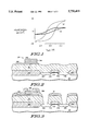
- the ferroelectric capacitor within a ferroelectric nonvolatile memory (FENVM) cell has a hysterisis curve 12 as illustrated in FIG. 1.
- Hysterisis curve represents an essentially ideal curve.
- P NV nonvolatile polarization
- a need also exists for achieving this solution without the use of complicated processing steps or the use of exotic materials.
- FIG. 1 includes a plot of polarization versus applied voltage for an ideal hysterisis curve and a hysterisis generally seen after forming a substantially completed device (prior art);
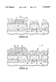
- FIG. 2 includes an illustration of a cross-sectional view of a portion of a semiconductor substrate after forming a ferroelectric capacitor
- FIG. 3 includes an illustration of the substrate of FIG. 2 after forming a patterned interlevel dielectric layer in accordance with an embodiment of the present invention
- FIG. 4 includes an illustration of a cross-sectional view of the substrate of FIG. 3 after forming interconnects
- FIG. 5 includes an illustration of a cross-sectional view of the substrate of FIG. 4 after forming a passivation layer in accordance with an embodiment of the present invention.
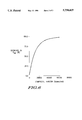
- FIG. 6 includes a plot of the decrease of nonvolatile polarization is plotted as a function of composite tension for films within a FENVM cell.
- One or more dielectric layers are formed over a ferroelectric capacitor of a FENVM cell, where the composite tension within the dielectric layers overlying the ferroelectric capacitor is kept relatively low. By keeping the tension relatively low, the nonvolatile polarization of the FENVM cell is maintained during back end processing steps of a fabrication process.
- the present invention is better understood with the description of the embodiments below.
- FIG. 2 includes an illustration of a semiconductor device substrate 20 after forming a ferroelectric capacitor 24. More specifically, the semiconductor device substrate 20 includes field isolation regions 202 and doped regions 204 that are formed within the substrate. As used in this specification, the semiconductor device substrate 20 includes a monocrystalline semiconductor wafer, a semiconductor-on-insulating wafer, or any other substrate used to form semiconductor devices.
- the field isolation regions 202 are formed using a selective oxidation process or in a trench isolation process.
- the doped regions 204 are heavily n-type regions that are source/drain regions for the FENVM cell.
- a gate dielectric layer 212 is formed over the substrate 20 and a gate electrode 214 is formed over the gate dielectric layer 212.
- the transistor is an n-channel MOS transistor. In other embodiments, a p-channel transistor or a bipolar transistor could be used. Insulating side wall spacers 216 are formed adjacent to the gate electrode 214.
- a first interlevel dielectric (ILD) layer 22 is then formed over all the substrate 20 as illustrated in FIG. 2.
- a ferroelectric capacitor 24 is formed over the first ILD layer 22.
- the ferroelectric capacitor 24 includes a first electrode 242, a ferroelectric dielectric layer 244, and a second electrode 246.
- the ferroelectric capacitor 24 is formed using conventional methods.
- a second ILD layer 32 is then formed over the ferroelectric capacitor 24 as illustrated in FIG. 3.
- the interlevel dielectric layer is typically formed of plasma tetraethylorthosilicate (plasma TEOS).
- plasma TEOS plasma tetraethylorthosilicate
- Contact openings are formed through the second ILD layer 32 to the lower electrode 242, the second electrode 246, and the doped regions 204.
- the etch sequence is performed using conventional methods.
- Interconnects 42 are formed over the semiconductor device substrate 20 as illustrated in FIG. 4.
- the interconnects 42 include aluminum, copper, or the like. Referring to FIG. 4, the interconnect near the right-hand side of the FIG. 4 is a bit line contact, the interconnect near the left-hand side of FIG. 4 is a drive line contact, and the middle interconnect is a conductive strap for the storage node and electrically connects one of the doped regions 204 to the second electrode 246 of the ferroelectric capacitor 24.
- a passivation layer 52 which is a dielectric layer covering the uppermost interconnect level of a semiconductor device, is formed over the interconnects 42 and the exposed portions of the interlevel dielectric layer 32.
- the passivation layer includes a lower tensile film 522 and an upper compressive film 524.
- the tensile film 522 is phosphosilicate glass (PSG)
- the compressive film 524 is silicon oxynitride.
- composite tension is the sum of the tensions within the individual dielectric layers including any film(s) within each dielectric layer.
- Tension is approximated using unpatterned silicon wafers. Stress, which has units of force per area, is measured at approximately room temperature after depositing a layer or film on the unpatterned silicon wafer. The stress is either tensile or compressive and is typically expressed in units of dynes per square centimeter. Tension, which has units of force per length and is typically expressed in units of dynes per centimeter, for a layer or film is a product of the stress times the thickness of the layer or film itself. Composite tension is the sum of the tensions within the individual layers or films.
- the composite tension should be no greater than approximately 2 ⁇ 10 4 dynes per centimeter (regardless whether the composite tension is tensile or compressive) or cause a decrease in P NV more than 75 percent from the initial P NV , which is the P NV of the ferroelectric capacitor after formation but before depositing any layers over the second electrode 246. Further, the tension within each layer should also be kept also below 2 ⁇ 10 4 dynes per centimeter.
- the tensions within each of the films can be higher than the 2 ⁇ 10 4 dynes per centimeter.
- the composite stress of the tensile film 522 and the compressive film 524 is no greater than 2 ⁇ 10 4 dynes per centimeter.
- the second ILD layer 32 can have a stress that is higher than 10 9 dynes per square centimeter.
- the interlevel dielectric layer could have a stress as high as 10 9 dynes per square centimeter and yet have a thickness of 1000 angstroms.
- the tension within the second ILD layer 32 that overlies the ferroelectric capacitor 24 is approximately 10 4 dynes per centimeter, which is lower than the 2 ⁇ 10 4 dynes per centimeter limit.
- the second ILD layer 32 should have a thickness less than 2000 angstroms to keep the tension below the limit.
- passivation layers have thicknesses of at least 6000 angstroms and usually more than 1.0 micron. If the passivation layer 52 has the same stress as the second ILD layer 32, the tension within the passivation layer 52 would exceed the limit. Therefore, high stress layers can be tolerated if their thicknesses are kept thin enough, but thicker layers will more strongly contribute to composite tension.
- the dual-film passivation layer 52 is tailored to reduce stress on the ferroelectric capacitor 24. Although the tension within each of the tensile and compressive films 522 and 524 may exceed 30 the tension limits, the composite tension within passivation layer 52 is within the composite tension limit because the tension within each film within the passivation layer 52 at least partially cancel out each other.
- most of the layers that include a combination of films, such as passivation layer 52, should have the tensile film underlying the compressive film because of a potential for the tensile film to absorb moisture, which can change the tension of the tensile film.
- a plurality of different films can form a single layer.
- a diffusion barrier is generally formed over the copper to prevent copper from diffusing into oxide.
- the diffusion barrier is typically a compressive film.
- the ferroelectric capacitor may be formed as a planar, vertically oriented ferroelectric capacitor within a trench.
- vertically oriented means that the capacitor plates are essentially perpendicular to the primary surface of the substrate.
- a trench is formed within a substrate.
- a dielectric layer having a vertical edge is formed within the trench of the substrate.
- the ferroelectric capacitor is formed near that vertical edge.
- lateral tension within the dielectric layer can compress the electrodes of the ferroelectric capacitor similar to a vise, thereby potentially causing the decreased P NV similar to the embodiment described in FIGS. 2 through 5.
- the dielectric layer within the trench should be formed such that its tension is no greater than 2 ⁇ 10 4 dynes per centimeter.
Landscapes
- Semiconductor Memories (AREA)
- Non-Volatile Memory (AREA)
Abstract
Description
Claims (23)
Priority Applications (4)
| Application Number | Priority Date | Filing Date | Title |
|---|---|---|---|
| US08/803,789 US5750419A (en) | 1997-02-24 | 1997-02-24 | Process for forming a semiconductor device having a ferroelectric capacitor |
| TW086118680A TW365044B (en) | 1997-02-24 | 1997-12-11 | Process for forming a semiconductor device |
| KR1019970078539A KR19980070271A (en) | 1997-02-24 | 1997-12-30 | Semiconductor device formation method |
| JP05884298A JP4086951B2 (en) | 1997-02-24 | 1998-02-24 | Method for forming a semiconductor device |
Applications Claiming Priority (1)
| Application Number | Priority Date | Filing Date | Title |
|---|---|---|---|
| US08/803,789 US5750419A (en) | 1997-02-24 | 1997-02-24 | Process for forming a semiconductor device having a ferroelectric capacitor |
Publications (1)
| Publication Number | Publication Date |
|---|---|
| US5750419A true US5750419A (en) | 1998-05-12 |
Family
ID=25187428
Family Applications (1)
| Application Number | Title | Priority Date | Filing Date |
|---|---|---|---|
| US08/803,789 Expired - Lifetime US5750419A (en) | 1997-02-24 | 1997-02-24 | Process for forming a semiconductor device having a ferroelectric capacitor |
Country Status (4)
| Country | Link |
|---|---|
| US (1) | US5750419A (en) |
| JP (1) | JP4086951B2 (en) |
| KR (1) | KR19980070271A (en) |
| TW (1) | TW365044B (en) |
Cited By (24)
| Publication number | Priority date | Publication date | Assignee | Title |
|---|---|---|---|---|
| GB2336468A (en) * | 1998-04-18 | 1999-10-20 | Samsung Electronics Co Ltd | Method for fabricating a ferroelectric memory device |
| US6022774A (en) * | 1997-03-19 | 2000-02-08 | Fujitsu Limited | Method for production of semiconductor device |
| EP0996160A1 (en) * | 1998-10-12 | 2000-04-26 | STMicroelectronics S.r.l. | Contact structure for a semiconductor device |
| US6080617A (en) * | 1992-06-12 | 2000-06-27 | Matsushita Electric Industrial Co., Ltd. | Semiconductor device having capacitor and manufacturing method thereof |
| US6153463A (en) * | 1999-07-09 | 2000-11-28 | Macronix International Co., Ltd. | Triple plate capacitor and method for manufacturing |
| US6171899B1 (en) * | 1999-03-12 | 2001-01-09 | United Microelectronics Corp. | Method for fabricating a capacitor |
| US6190926B1 (en) * | 1996-10-08 | 2001-02-20 | Ramtron International Corporation | Yield enhancement technique for integrated circuit processing to reduce effects of undesired dielectric moisture retention and subsequent hydrogen out-diffusion |
| US20020047111A1 (en) * | 1997-10-24 | 2002-04-25 | Yuji Judai | Semiconductor device having a ferroelectric capacitor with tensile stress properties |
| US6379977B1 (en) * | 1998-10-01 | 2002-04-30 | Hyundai Electronics Industries Co., Ltd. | Method of manufacturing ferroelectric memory device |
| US20020056861A1 (en) * | 1997-06-24 | 2002-05-16 | Yoshihisa Nagano | Semiconductor device and method for fabricating the same |
| KR100365715B1 (en) * | 1998-11-30 | 2002-12-26 | 닛뽕덴끼 가부시끼가이샤 | Ferroelectric memory device having a protective layer and manufacturing method thereof |
| US6579727B1 (en) | 1999-11-10 | 2003-06-17 | Stmicroelectronics S.R.L. | Process for selectively sealing ferroelectric capacitive elements incorporated in semiconductor integrated non-volatile memory cells |
| US6633060B2 (en) | 2000-11-17 | 2003-10-14 | Stmicroelectronics S.R.L. | Contact structure for a ferroelectric memory device |
| US20040077168A1 (en) * | 1997-07-16 | 2004-04-22 | Hidetoshi Ishida | Etchant and method for fabricating a semiconductor device using the same |
| US6734565B2 (en) | 2001-04-19 | 2004-05-11 | Stmicroelectronics S.R.L. | Contact structure for an integrated semiconductor device |
| US20040212041A1 (en) * | 2002-06-28 | 2004-10-28 | Fujitsu Limited | Semiconductor device and method of manufacturing the same |
| US20050009209A1 (en) * | 1999-11-10 | 2005-01-13 | Stmicroelectronics S.R.L. | Process for selectively sealing ferroelectric capactive elements incorporated in semiconductor integrated non-volatile memory cells |
| US20060214205A1 (en) * | 2005-03-28 | 2006-09-28 | Fujitsu Limited | Thin-film capacitor element and semiconductor device |
| US20070232014A1 (en) * | 2006-04-03 | 2007-10-04 | Honeywell International Inc. | Method of fabricating a planar MIM capacitor |
| US8723654B2 (en) | 2010-07-09 | 2014-05-13 | Cypress Semiconductor Corporation | Interrupt generation and acknowledgment for RFID |
| US8941218B1 (en) * | 2013-08-13 | 2015-01-27 | Avago Technologies General Ip (Singapore) Pte. Ltd. | Passivation for group III-V semiconductor devices having a plated metal layer over an interlayer dielectric layer |
| US9092582B2 (en) | 2010-07-09 | 2015-07-28 | Cypress Semiconductor Corporation | Low power, low pin count interface for an RFID transponder |
| US9846664B2 (en) | 2010-07-09 | 2017-12-19 | Cypress Semiconductor Corporation | RFID interface and interrupt |
| US12132044B2 (en) * | 2019-03-11 | 2024-10-29 | Samsung Electronics Co., Ltd. | Semiconductor device including an upper contact in contact with a side surface of an upper gate structure |
Citations (14)
| Publication number | Priority date | Publication date | Assignee | Title |
|---|---|---|---|---|
| US4091407A (en) * | 1976-11-01 | 1978-05-23 | Rca Corporation | Combination glass/low temperature deposited Siw Nx Hy O.sub.z |
| US4091406A (en) * | 1976-11-01 | 1978-05-23 | Rca Corporation | Combination glass/low temperature deposited Siw Nx Hy O.sub.z |
| US4097889A (en) * | 1976-11-01 | 1978-06-27 | Rca Corporation | Combination glass/low temperature deposited Siw Nx Hy O.sub.z |
| JPS5873124A (en) * | 1981-10-26 | 1983-05-02 | Fujitsu Ltd | Semiconductor device |
| US4446194A (en) * | 1982-06-21 | 1984-05-01 | Motorola, Inc. | Dual layer passivation |
| US4620986A (en) * | 1984-11-09 | 1986-11-04 | Intel Corporation | MOS rear end processing |
| US4625227A (en) * | 1980-09-01 | 1986-11-25 | Hitachi, Ltd | Resin molded type semiconductor device having a conductor film |
| US4733289A (en) * | 1980-04-25 | 1988-03-22 | Hitachi, Ltd. | Resin-molded semiconductor device using polyimide and nitride films for the passivation film |
| US5046043A (en) * | 1987-10-08 | 1991-09-03 | National Semiconductor Corporation | Ferroelectric capacitor and memory cell including barrier and isolation layers |
| US5327012A (en) * | 1990-03-27 | 1994-07-05 | Matsushita Electric Industrial Co., Ltd. | Semiconductor device having a double-layer interconnection structure |
| US5401680A (en) * | 1992-02-18 | 1995-03-28 | National Semiconductor Corporation | Method for forming a ceramic oxide capacitor having barrier layers |
| US5439840A (en) * | 1993-08-02 | 1995-08-08 | Motorola, Inc. | Method of forming a nonvolatile random access memory capacitor cell having a metal-oxide dielectric |
| US5583077A (en) * | 1995-04-04 | 1996-12-10 | Taiwan Semiconductor Manufacturing Company Ltd | Integrated dual layer passivation process to suppress stress-induced metal voids |
| US5624864A (en) * | 1993-08-05 | 1997-04-29 | Matsushita Electronics Corporation | Semiconductor device having capacitor and manufacturing method thereof |
-
1997
- 1997-02-24 US US08/803,789 patent/US5750419A/en not_active Expired - Lifetime
- 1997-12-11 TW TW086118680A patent/TW365044B/en not_active IP Right Cessation
- 1997-12-30 KR KR1019970078539A patent/KR19980070271A/en not_active Withdrawn
-
1998
- 1998-02-24 JP JP05884298A patent/JP4086951B2/en not_active Expired - Lifetime
Patent Citations (14)
| Publication number | Priority date | Publication date | Assignee | Title |
|---|---|---|---|---|
| US4091406A (en) * | 1976-11-01 | 1978-05-23 | Rca Corporation | Combination glass/low temperature deposited Siw Nx Hy O.sub.z |
| US4097889A (en) * | 1976-11-01 | 1978-06-27 | Rca Corporation | Combination glass/low temperature deposited Siw Nx Hy O.sub.z |
| US4091407A (en) * | 1976-11-01 | 1978-05-23 | Rca Corporation | Combination glass/low temperature deposited Siw Nx Hy O.sub.z |
| US4733289A (en) * | 1980-04-25 | 1988-03-22 | Hitachi, Ltd. | Resin-molded semiconductor device using polyimide and nitride films for the passivation film |
| US4625227A (en) * | 1980-09-01 | 1986-11-25 | Hitachi, Ltd | Resin molded type semiconductor device having a conductor film |
| JPS5873124A (en) * | 1981-10-26 | 1983-05-02 | Fujitsu Ltd | Semiconductor device |
| US4446194A (en) * | 1982-06-21 | 1984-05-01 | Motorola, Inc. | Dual layer passivation |
| US4620986A (en) * | 1984-11-09 | 1986-11-04 | Intel Corporation | MOS rear end processing |
| US5046043A (en) * | 1987-10-08 | 1991-09-03 | National Semiconductor Corporation | Ferroelectric capacitor and memory cell including barrier and isolation layers |
| US5327012A (en) * | 1990-03-27 | 1994-07-05 | Matsushita Electric Industrial Co., Ltd. | Semiconductor device having a double-layer interconnection structure |
| US5401680A (en) * | 1992-02-18 | 1995-03-28 | National Semiconductor Corporation | Method for forming a ceramic oxide capacitor having barrier layers |
| US5439840A (en) * | 1993-08-02 | 1995-08-08 | Motorola, Inc. | Method of forming a nonvolatile random access memory capacitor cell having a metal-oxide dielectric |
| US5624864A (en) * | 1993-08-05 | 1997-04-29 | Matsushita Electronics Corporation | Semiconductor device having capacitor and manufacturing method thereof |
| US5583077A (en) * | 1995-04-04 | 1996-12-10 | Taiwan Semiconductor Manufacturing Company Ltd | Integrated dual layer passivation process to suppress stress-induced metal voids |
Non-Patent Citations (3)
| Title |
|---|
| Stanley Wolf Ph.D, "Silicon Processing for the VLSI Era", vol. 2: Process Integration, Lattice Press 1990, Semiconductor Memory Process Integration., pp. 635-638. |
| Stanley Wolf Ph.D, Silicon Processing for the VLSI Era , vol. 2: Process Integration, Lattice Press 1990, Semiconductor Memory Process Integration., pp. 635 638. * |
| Sze, VLSI technology, pp. 116, 119, 123, 1983. * |
Cited By (34)
| Publication number | Priority date | Publication date | Assignee | Title |
|---|---|---|---|---|
| US6080617A (en) * | 1992-06-12 | 2000-06-27 | Matsushita Electric Industrial Co., Ltd. | Semiconductor device having capacitor and manufacturing method thereof |
| US6190926B1 (en) * | 1996-10-08 | 2001-02-20 | Ramtron International Corporation | Yield enhancement technique for integrated circuit processing to reduce effects of undesired dielectric moisture retention and subsequent hydrogen out-diffusion |
| US6022774A (en) * | 1997-03-19 | 2000-02-08 | Fujitsu Limited | Method for production of semiconductor device |
| US20050082638A1 (en) * | 1997-06-24 | 2005-04-21 | Yoshihisa Nagano | Semiconductor device and method for fabricating the same |
| US6849887B2 (en) * | 1997-06-24 | 2005-02-01 | Matsushita Electric Industrial Co., Ltd. | Semiconductor device and method for fabricating the same |
| US20020056861A1 (en) * | 1997-06-24 | 2002-05-16 | Yoshihisa Nagano | Semiconductor device and method for fabricating the same |
| US20040077168A1 (en) * | 1997-07-16 | 2004-04-22 | Hidetoshi Ishida | Etchant and method for fabricating a semiconductor device using the same |
| US20020047111A1 (en) * | 1997-10-24 | 2002-04-25 | Yuji Judai | Semiconductor device having a ferroelectric capacitor with tensile stress properties |
| GB2336468A (en) * | 1998-04-18 | 1999-10-20 | Samsung Electronics Co Ltd | Method for fabricating a ferroelectric memory device |
| US6379977B1 (en) * | 1998-10-01 | 2002-04-30 | Hyundai Electronics Industries Co., Ltd. | Method of manufacturing ferroelectric memory device |
| US6737284B2 (en) | 1998-10-12 | 2004-05-18 | Stmicroelectronics S.R.L. | Contact structure for semiconductor devices and corresponding manufacturing process |
| US6541808B2 (en) | 1998-10-12 | 2003-04-01 | Raffaele Zambrano | Contact structure for semiconductor devices and corresponding manufacturing process |
| US20030082873A1 (en) * | 1998-10-12 | 2003-05-01 | Stmicroelectronics S.R.I. | Contact structure for semiconductor devices and corresponding manufacturing process |
| EP0996160A1 (en) * | 1998-10-12 | 2000-04-26 | STMicroelectronics S.r.l. | Contact structure for a semiconductor device |
| KR100365715B1 (en) * | 1998-11-30 | 2002-12-26 | 닛뽕덴끼 가부시끼가이샤 | Ferroelectric memory device having a protective layer and manufacturing method thereof |
| US6171899B1 (en) * | 1999-03-12 | 2001-01-09 | United Microelectronics Corp. | Method for fabricating a capacitor |
| US6153463A (en) * | 1999-07-09 | 2000-11-28 | Macronix International Co., Ltd. | Triple plate capacitor and method for manufacturing |
| US6579727B1 (en) | 1999-11-10 | 2003-06-17 | Stmicroelectronics S.R.L. | Process for selectively sealing ferroelectric capacitive elements incorporated in semiconductor integrated non-volatile memory cells |
| US20050009209A1 (en) * | 1999-11-10 | 2005-01-13 | Stmicroelectronics S.R.L. | Process for selectively sealing ferroelectric capactive elements incorporated in semiconductor integrated non-volatile memory cells |
| US20040005725A1 (en) * | 2000-11-17 | 2004-01-08 | Stmicroelectronics S.R.L. | Method of forming a contact structure and a ferroelectric memory device |
| US6633060B2 (en) | 2000-11-17 | 2003-10-14 | Stmicroelectronics S.R.L. | Contact structure for a ferroelectric memory device |
| US6878982B2 (en) | 2000-11-17 | 2005-04-12 | Stmicroelectronics S.R.L. | Method of forming a contact structure and a ferroelectric memory device |
| US20040175927A1 (en) * | 2001-04-19 | 2004-09-09 | Stmicroelectronics S.R.I. | Contact structure for an integrated semiconductor device |
| US6734565B2 (en) | 2001-04-19 | 2004-05-11 | Stmicroelectronics S.R.L. | Contact structure for an integrated semiconductor device |
| US7052985B2 (en) | 2001-04-19 | 2006-05-30 | Stmicroelectronics S.R.L. | Contact structure for an integrated semiconductor device |
| US20040212041A1 (en) * | 2002-06-28 | 2004-10-28 | Fujitsu Limited | Semiconductor device and method of manufacturing the same |
| US20060214205A1 (en) * | 2005-03-28 | 2006-09-28 | Fujitsu Limited | Thin-film capacitor element and semiconductor device |
| US20070232014A1 (en) * | 2006-04-03 | 2007-10-04 | Honeywell International Inc. | Method of fabricating a planar MIM capacitor |
| US8723654B2 (en) | 2010-07-09 | 2014-05-13 | Cypress Semiconductor Corporation | Interrupt generation and acknowledgment for RFID |
| US9092582B2 (en) | 2010-07-09 | 2015-07-28 | Cypress Semiconductor Corporation | Low power, low pin count interface for an RFID transponder |
| US9846664B2 (en) | 2010-07-09 | 2017-12-19 | Cypress Semiconductor Corporation | RFID interface and interrupt |
| US8941218B1 (en) * | 2013-08-13 | 2015-01-27 | Avago Technologies General Ip (Singapore) Pte. Ltd. | Passivation for group III-V semiconductor devices having a plated metal layer over an interlayer dielectric layer |
| US20150048484A1 (en) * | 2013-08-13 | 2015-02-19 | Avago Technologies General Ip (Singapore) Pte. Ltd. | Passivation for Group III-V Semiconductor Devices Having a Plated Metal Layer over an Interlayer Dielectric Layer |
| US12132044B2 (en) * | 2019-03-11 | 2024-10-29 | Samsung Electronics Co., Ltd. | Semiconductor device including an upper contact in contact with a side surface of an upper gate structure |
Also Published As
| Publication number | Publication date |
|---|---|
| JPH10270655A (en) | 1998-10-09 |
| TW365044B (en) | 1999-07-21 |
| JP4086951B2 (en) | 2008-05-14 |
| KR19980070271A (en) | 1998-10-26 |
Similar Documents
| Publication | Publication Date | Title |
|---|---|---|
| US5750419A (en) | Process for forming a semiconductor device having a ferroelectric capacitor | |
| US11903191B2 (en) | Embedded flash memory device with floating gate embedded in a substrate | |
| US7060552B2 (en) | Memory device with hydrogen-blocked ferroelectric capacitor | |
| US5728595A (en) | Method of fabricating a self-aligned contact hole for a semiconductor device | |
| US6982453B2 (en) | Semicondutor device having ferroelectric capacitor and hydrogen barrier film and manufacturing method thereof | |
| US6150184A (en) | Method of fabricating partially or completely encapsulated top electrode of a ferroelectric capacitor | |
| US6462371B1 (en) | Films doped with carbon for use in integrated circuit technology | |
| US20010001488A1 (en) | Completely encapsulated top electrode of a ferroelectric capacitor using a lead-enhanced encapsulation layer | |
| JPH0737988A (en) | Method for manufacturing semiconductor integrated circuit device | |
| US20050090023A1 (en) | Method of forming ferroelectric memory cell | |
| US5518947A (en) | Method of forming a semiconductor memory device having silicon nitride overlying only in peripheral circuit area | |
| US6486506B1 (en) | Flash memory with less susceptibility to charge gain and charge loss | |
| US6908868B2 (en) | Gas passivation on nitride encapsulated devices | |
| US6228701B1 (en) | Apparatus and method for minimizing diffusion in stacked capacitors formed on silicon plugs | |
| US6232194B1 (en) | Silicon nitride capped poly resistor with SAC process | |
| US6967368B2 (en) | Ferro-electric memory device and method of manufacturing the same | |
| US6858442B2 (en) | Ferroelectric memory integrated circuit with improved reliability | |
| US6933549B2 (en) | Barrier material | |
| US20060214218A1 (en) | Semiconductor device and method of fabricating the same | |
| JPH1187651A (en) | Semiconductor integrated circuit device and method of manufacturing the same | |
| TWI893358B (en) | Integrated chip and method of forming the same | |
| JP2820065B2 (en) | Method for manufacturing semiconductor device | |
| JPH10294432A (en) | Ferroelectric capacitor, ferroelectric nonvolatile memory device, and ferroelectric device | |
| JPH10321719A (en) | Semiconductor integrated circuit device and method of manufacturing the same | |
| US6974989B1 (en) | Structure and method for protecting memory cells from UV radiation damage and UV radiation-induced charging during backend processing |
Legal Events
| Date | Code | Title | Description |
|---|---|---|---|
| STCF | Information on status: patent grant |
Free format text: PATENTED CASE |
|
| CC | Certificate of correction | ||
| FPAY | Fee payment |
Year of fee payment: 4 |
|
| AS | Assignment |
Owner name: FREESCALE SEMICONDUCTOR, INC., TEXAS Free format text: ASSIGNMENT OF ASSIGNORS INTEREST;ASSIGNOR:MOTOROLA, INC.;REEL/FRAME:015698/0657 Effective date: 20040404 Owner name: FREESCALE SEMICONDUCTOR, INC.,TEXAS Free format text: ASSIGNMENT OF ASSIGNORS INTEREST;ASSIGNOR:MOTOROLA, INC.;REEL/FRAME:015698/0657 Effective date: 20040404 |
|
| FPAY | Fee payment |
Year of fee payment: 8 |
|
| AS | Assignment |
Owner name: CITIBANK, N.A. AS COLLATERAL AGENT, NEW YORK Free format text: SECURITY AGREEMENT;ASSIGNORS:FREESCALE SEMICONDUCTOR, INC.;FREESCALE ACQUISITION CORPORATION;FREESCALE ACQUISITION HOLDINGS CORP.;AND OTHERS;REEL/FRAME:018855/0129 Effective date: 20061201 Owner name: CITIBANK, N.A. AS COLLATERAL AGENT,NEW YORK Free format text: SECURITY AGREEMENT;ASSIGNORS:FREESCALE SEMICONDUCTOR, INC.;FREESCALE ACQUISITION CORPORATION;FREESCALE ACQUISITION HOLDINGS CORP.;AND OTHERS;REEL/FRAME:018855/0129 Effective date: 20061201 |
|
| FPAY | Fee payment |
Year of fee payment: 12 |
|
| AS | Assignment |
Owner name: CITIBANK, N.A., AS COLLATERAL AGENT,NEW YORK Free format text: SECURITY AGREEMENT;ASSIGNOR:FREESCALE SEMICONDUCTOR, INC.;REEL/FRAME:024397/0001 Effective date: 20100413 Owner name: CITIBANK, N.A., AS COLLATERAL AGENT, NEW YORK Free format text: SECURITY AGREEMENT;ASSIGNOR:FREESCALE SEMICONDUCTOR, INC.;REEL/FRAME:024397/0001 Effective date: 20100413 |
|
| AS | Assignment |
Owner name: CITIBANK, N.A., AS NOTES COLLATERAL AGENT, NEW YORK Free format text: SECURITY AGREEMENT;ASSIGNOR:FREESCALE SEMICONDUCTOR, INC.;REEL/FRAME:030633/0424 Effective date: 20130521 Owner name: CITIBANK, N.A., AS NOTES COLLATERAL AGENT, NEW YOR Free format text: SECURITY AGREEMENT;ASSIGNOR:FREESCALE SEMICONDUCTOR, INC.;REEL/FRAME:030633/0424 Effective date: 20130521 |
|
| AS | Assignment |
Owner name: CITIBANK, N.A., AS NOTES COLLATERAL AGENT, NEW YORK Free format text: SECURITY AGREEMENT;ASSIGNOR:FREESCALE SEMICONDUCTOR, INC.;REEL/FRAME:031591/0266 Effective date: 20131101 Owner name: CITIBANK, N.A., AS NOTES COLLATERAL AGENT, NEW YOR Free format text: SECURITY AGREEMENT;ASSIGNOR:FREESCALE SEMICONDUCTOR, INC.;REEL/FRAME:031591/0266 Effective date: 20131101 |
|
| AS | Assignment |
Owner name: FREESCALE SEMICONDUCTOR, INC., TEXAS Free format text: PATENT RELEASE;ASSIGNOR:CITIBANK, N.A., AS COLLATERAL AGENT;REEL/FRAME:037354/0225 Effective date: 20151207 Owner name: FREESCALE SEMICONDUCTOR, INC., TEXAS Free format text: PATENT RELEASE;ASSIGNOR:CITIBANK, N.A., AS COLLATERAL AGENT;REEL/FRAME:037356/0143 Effective date: 20151207 Owner name: FREESCALE SEMICONDUCTOR, INC., TEXAS Free format text: PATENT RELEASE;ASSIGNOR:CITIBANK, N.A., AS COLLATERAL AGENT;REEL/FRAME:037356/0553 Effective date: 20151207 |
|
| AS | Assignment |
Owner name: MORGAN STANLEY SENIOR FUNDING, INC., MARYLAND Free format text: ASSIGNMENT AND ASSUMPTION OF SECURITY INTEREST IN PATENTS;ASSIGNOR:CITIBANK, N.A.;REEL/FRAME:037486/0517 Effective date: 20151207 |
|
| AS | Assignment |
Owner name: MORGAN STANLEY SENIOR FUNDING, INC., MARYLAND Free format text: ASSIGNMENT AND ASSUMPTION OF SECURITY INTEREST IN PATENTS;ASSIGNOR:CITIBANK, N.A.;REEL/FRAME:037518/0292 Effective date: 20151207 |
|
| AS | Assignment |
Owner name: MORGAN STANLEY SENIOR FUNDING, INC., MARYLAND Free format text: SUPPLEMENT TO THE SECURITY AGREEMENT;ASSIGNOR:FREESCALE SEMICONDUCTOR, INC.;REEL/FRAME:039138/0001 Effective date: 20160525 |
|
| AS | Assignment |
Owner name: NXP, B.V., F/K/A FREESCALE SEMICONDUCTOR, INC., NETHERLANDS Free format text: RELEASE BY SECURED PARTY;ASSIGNOR:MORGAN STANLEY SENIOR FUNDING, INC.;REEL/FRAME:040925/0001 Effective date: 20160912 Owner name: NXP, B.V., F/K/A FREESCALE SEMICONDUCTOR, INC., NE Free format text: RELEASE BY SECURED PARTY;ASSIGNOR:MORGAN STANLEY SENIOR FUNDING, INC.;REEL/FRAME:040925/0001 Effective date: 20160912 |
|
| AS | Assignment |
Owner name: NXP B.V., NETHERLANDS Free format text: RELEASE BY SECURED PARTY;ASSIGNOR:MORGAN STANLEY SENIOR FUNDING, INC.;REEL/FRAME:040928/0001 Effective date: 20160622 |
|
| AS | Assignment |
Owner name: NXP USA, INC., TEXAS Free format text: CHANGE OF NAME;ASSIGNOR:FREESCALE SEMICONDUCTOR INC.;REEL/FRAME:040652/0180 Effective date: 20161107 |
|
| AS | Assignment |
Owner name: NXP USA, INC., TEXAS Free format text: CORRECTIVE ASSIGNMENT TO CORRECT THE NATURE OF CONVEYANCE LISTED CHANGE OF NAME SHOULD BE MERGER AND CHANGE PREVIOUSLY RECORDED AT REEL: 040652 FRAME: 0180. ASSIGNOR(S) HEREBY CONFIRMS THE MERGER AND CHANGE OF NAME;ASSIGNOR:FREESCALE SEMICONDUCTOR INC.;REEL/FRAME:041354/0148 Effective date: 20161107 |
|
| AS | Assignment |
Owner name: MORGAN STANLEY SENIOR FUNDING, INC., MARYLAND Free format text: CORRECTIVE ASSIGNMENT TO CORRECT THE REMOVE PATENTS 8108266 AND 8062324 AND REPLACE THEM WITH 6108266 AND 8060324 PREVIOUSLY RECORDED ON REEL 037518 FRAME 0292. ASSIGNOR(S) HEREBY CONFIRMS THE ASSIGNMENT AND ASSUMPTION OF SECURITY INTEREST IN PATENTS;ASSIGNOR:CITIBANK, N.A.;REEL/FRAME:041703/0536 Effective date: 20151207 |
|
| AS | Assignment |
Owner name: SHENZHEN XINGUODU TECHNOLOGY CO., LTD., CHINA Free format text: CORRECTIVE ASSIGNMENT TO CORRECT THE TO CORRECT THE APPLICATION NO. FROM 13,883,290 TO 13,833,290 PREVIOUSLY RECORDED ON REEL 041703 FRAME 0536. ASSIGNOR(S) HEREBY CONFIRMS THE THE ASSIGNMENT AND ASSUMPTION OF SECURITYINTEREST IN PATENTS.;ASSIGNOR:MORGAN STANLEY SENIOR FUNDING, INC.;REEL/FRAME:048734/0001 Effective date: 20190217 Owner name: SHENZHEN XINGUODU TECHNOLOGY CO., LTD., CHINA Free format text: CORRECTIVE ASSIGNMENT TO CORRECT THE TO CORRECT THE APPLICATION NO. FROM 13,883,290 TO 13,833,290 PREVIOUSLY RECORDED ON REEL 041703 FRAME 0536. ASSIGNOR(S) HEREBY CONFIRMS THE THE ASSIGNMENT AND ASSUMPTION OF SECURITY INTEREST IN PATENTS.;ASSIGNOR:MORGAN STANLEY SENIOR FUNDING, INC.;REEL/FRAME:048734/0001 Effective date: 20190217 |
|
| AS | Assignment |
Owner name: NXP B.V., NETHERLANDS Free format text: RELEASE BY SECURED PARTY;ASSIGNOR:MORGAN STANLEY SENIOR FUNDING, INC.;REEL/FRAME:050744/0097 Effective date: 20190903 |
|
| AS | Assignment |
Owner name: MORGAN STANLEY SENIOR FUNDING, INC., MARYLAND Free format text: CORRECTIVE ASSIGNMENT TO CORRECT THE REMOVE APPLICATION11759915 AND REPLACE IT WITH APPLICATION 11759935 PREVIOUSLY RECORDED ON REEL 037486 FRAME 0517. ASSIGNOR(S) HEREBY CONFIRMS THE ASSIGNMENT AND ASSUMPTION OF SECURITYINTEREST IN PATENTS;ASSIGNOR:CITIBANK, N.A.;REEL/FRAME:053547/0421 Effective date: 20151207 Owner name: MORGAN STANLEY SENIOR FUNDING, INC., MARYLAND Free format text: CORRECTIVE ASSIGNMENT TO CORRECT THE REMOVE APPLICATION 11759915 AND REPLACE IT WITH APPLICATION 11759935 PREVIOUSLY RECORDED ON REEL 037486 FRAME 0517. ASSIGNOR(S) HEREBY CONFIRMS THE ASSIGNMENT AND ASSUMPTION OF SECURITY INTEREST IN PATENTS;ASSIGNOR:CITIBANK, N.A.;REEL/FRAME:053547/0421 Effective date: 20151207 |
|
| AS | Assignment |
Owner name: NXP B.V., NETHERLANDS Free format text: CORRECTIVE ASSIGNMENT TO CORRECT THE REMOVEAPPLICATION 11759915 AND REPLACE IT WITH APPLICATION11759935 PREVIOUSLY RECORDED ON REEL 040928 FRAME 0001. ASSIGNOR(S) HEREBY CONFIRMS THE RELEASE OF SECURITYINTEREST;ASSIGNOR:MORGAN STANLEY SENIOR FUNDING, INC.;REEL/FRAME:052915/0001 Effective date: 20160622 Owner name: NXP B.V., NETHERLANDS Free format text: CORRECTIVE ASSIGNMENT TO CORRECT THE REMOVE APPLICATION 11759915 AND REPLACE IT WITH APPLICATION 11759935 PREVIOUSLY RECORDED ON REEL 040928 FRAME 0001. ASSIGNOR(S) HEREBY CONFIRMS THE RELEASE OF SECURITY INTEREST;ASSIGNOR:MORGAN STANLEY SENIOR FUNDING, INC.;REEL/FRAME:052915/0001 Effective date: 20160622 |
|
| AS | Assignment |
Owner name: NXP, B.V. F/K/A FREESCALE SEMICONDUCTOR, INC., NETHERLANDS Free format text: CORRECTIVE ASSIGNMENT TO CORRECT THE REMOVEAPPLICATION 11759915 AND REPLACE IT WITH APPLICATION11759935 PREVIOUSLY RECORDED ON REEL 040925 FRAME 0001. ASSIGNOR(S) HEREBY CONFIRMS THE RELEASE OF SECURITYINTEREST;ASSIGNOR:MORGAN STANLEY SENIOR FUNDING, INC.;REEL/FRAME:052917/0001 Effective date: 20160912 Owner name: NXP, B.V. F/K/A FREESCALE SEMICONDUCTOR, INC., NETHERLANDS Free format text: CORRECTIVE ASSIGNMENT TO CORRECT THE REMOVE APPLICATION 11759915 AND REPLACE IT WITH APPLICATION 11759935 PREVIOUSLY RECORDED ON REEL 040925 FRAME 0001. ASSIGNOR(S) HEREBY CONFIRMS THE RELEASE OF SECURITY INTEREST;ASSIGNOR:MORGAN STANLEY SENIOR FUNDING, INC.;REEL/FRAME:052917/0001 Effective date: 20160912 |