EP0784346A2 - Ladungsübertragungsanordnung und Verwendung in einem Festkörperbildaufnahmegerät - Google Patents
Ladungsübertragungsanordnung und Verwendung in einem Festkörperbildaufnahmegerät Download PDFInfo
- Publication number
- EP0784346A2 EP0784346A2 EP97400040A EP97400040A EP0784346A2 EP 0784346 A2 EP0784346 A2 EP 0784346A2 EP 97400040 A EP97400040 A EP 97400040A EP 97400040 A EP97400040 A EP 97400040A EP 0784346 A2 EP0784346 A2 EP 0784346A2
- Authority
- EP
- European Patent Office
- Prior art keywords
- gate electrodes
- transfer
- groups
- group
- clock
- Prior art date
- Legal status (The legal status is an assumption and is not a legal conclusion. Google has not performed a legal analysis and makes no representation as to the accuracy of the status listed.)
- Withdrawn
Links
- 238000003384 imaging method Methods 0.000 title claims abstract description 22
- 238000009792 diffusion process Methods 0.000 claims description 5
- 150000002500 ions Chemical class 0.000 claims description 5
- 239000000758 substrate Substances 0.000 claims description 5
- 239000007943 implant Substances 0.000 claims 1
- 108091006146 Channels Proteins 0.000 abstract description 11
- 102000004129 N-Type Calcium Channels Human genes 0.000 abstract description 6
- 108090000699 N-Type Calcium Channels Proteins 0.000 abstract description 6
- 238000010438 heat treatment Methods 0.000 abstract description 5
- 230000003071 parasitic effect Effects 0.000 abstract description 5
- 230000003247 decreasing effect Effects 0.000 abstract description 4
- 238000010586 diagram Methods 0.000 description 10
- 238000001444 catalytic combustion detection Methods 0.000 description 8
- 230000003111 delayed effect Effects 0.000 description 4
- 238000000034 method Methods 0.000 description 4
- 230000004048 modification Effects 0.000 description 3
- 238000012986 modification Methods 0.000 description 3
- 230000008859 change Effects 0.000 description 2
- 229910021420 polycrystalline silicon Inorganic materials 0.000 description 2
- 229920005591 polysilicon Polymers 0.000 description 2
- 239000004065 semiconductor Substances 0.000 description 2
- 239000003990 capacitor Substances 0.000 description 1
- 230000000694 effects Effects 0.000 description 1
- 230000002708 enhancing effect Effects 0.000 description 1
- 238000012423 maintenance Methods 0.000 description 1
- 239000011159 matrix material Substances 0.000 description 1
- 230000000630 rising effect Effects 0.000 description 1
- 239000007787 solid Substances 0.000 description 1
- 230000007704 transition Effects 0.000 description 1
Images


Classifications
-
- H—ELECTRICITY
- H01—ELECTRIC ELEMENTS
- H01L—SEMICONDUCTOR DEVICES NOT COVERED BY CLASS H10
- H01L27/00—Devices consisting of a plurality of semiconductor or other solid-state components formed in or on a common substrate
- H01L27/14—Devices consisting of a plurality of semiconductor or other solid-state components formed in or on a common substrate including semiconductor components sensitive to infrared radiation, light, electromagnetic radiation of shorter wavelength or corpuscular radiation and specially adapted either for the conversion of the energy of such radiation into electrical energy or for the control of electrical energy by such radiation
- H01L27/144—Devices controlled by radiation
- H01L27/146—Imager structures
- H01L27/148—Charge coupled imagers
- H01L27/14831—Area CCD imagers
Definitions
- the present invention relates generally to a charge transfer device and a solid state imaging apparatus using this device. More particularly, the invention relates to a charge transfer device using a high-frequency clock of 10 MHz or higher as a transfer clock. The invention also relates to a solid-state imaging apparatus using this device as a horizontal transfer register.
- Fig. 7 is a sectional view of a conventional horizontal transfer register for use in a CCD-type solid-state imaging apparatus.
- an N-type channel 73 is formed on the obverse surface of an N-type semiconductor substrate 71 across a P-type well 72.
- First-layer and second-layer gate electrodes 74 and 75 formed of polysilicon or the like are repeatedly disposed in an alternating sequence above the N-type channel 73 through a gate insulating film (not shown).
- N - -ions are implanted under the gate electrodes 75 so as to form a storage region and a transfer region under the gate electrodes 74 and 75, respectively.
- Two-phase horizontal transfer clocks H ⁇ 1 and H ⁇ 2, as shown in Fig. 8, are alternately applied to the pairs of gate electrodes 74 and 75.
- the potential statuses at the timings t 1 through t 3 of applying these horizontal transfer clocks H ⁇ 1 and H ⁇ 2 to the gate electrodes 74 and 75 are illustrated in Fig. 9.
- the potential well under the gate electrodes 74 and 75 to which the clock H ⁇ 2 is applied becomes deeper, and more particularly, the portion below the gate electrode 74 (the storage region) has a larger potential than the portion below the gate electrode 75 (the transfer region), thereby causing signal charges to accumulate under the gate electrode 74 to which the clock H ⁇ 2 is applied.
- the horizontal transfer clock H ⁇ 1 is changed to the "H" level, while the horizontal transfer clock H ⁇ 2 undergoes a transition to the "L" level.
- the potential well of the gate electrodes 74 and 75 supplied with the clock H ⁇ 1 becomes even deeper, while the potential well of the gate electrodes 74 and 75 with the clock H ⁇ 2 becomes even shallower.
- the potential well under the gate electrode 74 having the clock H ⁇ 2 is shallower than the potential well under the gate electrode 75 supplied with the clock H ⁇ 1.
- the potential well under the gate electrode 74 to which the clock H ⁇ 1 is applied is deeper than the potential well under the gate electrode supplied with the clock H ⁇ 1.
- the above-described two-phase horizontal transfer register requires two-phase horizontal transfer clocks H ⁇ 1 and H ⁇ 2 in order to transfer signal charges.
- a large number of clocks disadvantageously increases power consumption, the amount of heating and the number of terminals.
- the storage region and the transfer region are required to be formed separately, which requires an extra process step, thereby increasing the number of process steps.
- signal charges can accumulate only under the gate electrodes 74 (the storage region) supplied with either of the horizontal transfer clocks H ⁇ 1 and H ⁇ 2 at the "H" level. This limits the region in which signal charges can accumulate to approximately one-fourth of the overall transfer length of the horizontal transfer register.
- a charge transfer device comprising: three groups of gate electrodes repeatedly disposed in an alternating sequence in the transfer direction above a transfer channel; first means for fixing the potential under one group of gate electrodes among the three groups of gate electrodes substantially at an intermediate level positioned between the maximum level and the minimum level of the respective potentials under the remaining two groups of gate electrodes to which transfer clocks are supplied; second means for supplying a single-phase transfer clock to one of the remaining two groups of gate electrodes; and third means for supplying the other group of gate electrodes with a transfer clock produced by delaying the single-phase transfer clock by a predetermined delay time.
- a solid-state imaging apparatus using a charge transfer device as a transfer register comprising: three groups of gate electrodes repeatedly disposed in an alternating sequence in the transfer direction above a transfer channel; first means for fixing the potential under one group of gate electrodes among the three groups of gate electrodes substantially at an intermediate level positioned between the maximum level and the minimum level of the respective potentials under the remaining two groups of gate electrodes to which transfer clocks are supplied; second means for supplying a single-phase transfer clock to one of the remaining two groups of gate electrodes; and third means for supplying the other group of gate electrodes with a transfer clock produced by delaying the single-phase transfer clock by a predetermined delay time.
- a charge transfer device comprising: three groups of gate electrodes repeatedly disposed in an alternating sequence in the transfer direction above a transfer channel; means for applying a predetermined bias voltage to one group of the three groups of gate electrodes; and means for supplying a single-phase transfer clock to one of the remaining two groups of gate electrodes and for supplying the other group of gate electrodes with a transfer clock generated by delaying the single-phase transfer clock by a predetermined delay time.
- a solid-state imaging apparatus comprising an imaging section including a plurality of photoelectric transducers for converting incident light into signal charges, and a charge transfer section for transferring the signal charges read from the plurality of photoelectric transducers, the charge transfer section comprising: three groups of gate electrodes repeatedly disposed in an alternating sequence in the transfer direction above a transfer channel; means for applying a predetermined bias voltage to one group of the three groups of gate electrodes; and means for supplying a single-phase transfer clock to one of the remaining two groups of gate electrodes and for supplying the other group of gate electrodes with a transfer clock generated by delaying the single-phase transfer clock by a predetermined delay time.
- a predetermined bias voltage is applied to one group of the three groups of electrodes.
- the bias voltage is determined so that the potential under the above group of electrodes can be maintained substantially at an intermediate level between the maximum level and the minimum level of the respective potentials under the remaining two groups of electrodes.
- a single-phase transfer clock supplied from the exterior of the device is directly fed to one of the remaining groups of electrodes, while a transfer clock produced by delaying the above single-phase transfer clock by a predetermined delay time is supplied to the other group of electrodes.
- three-phase transfer driving can be implemented while only requiring the single-phase transfer clock supplied from the exterior of the device.
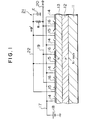
- an N-type channel 13 is formed on the obverse surface of an N-type semiconductor substrate 11 across a P-type well 12.
- a gate insulating film (not shown) in an alternating sequence in the charge transfer direction are, for example, three groups of gate electrodes, i.e., the first, second and third groups, indicated by 14, 15 and 16.
- These three groups of gate electrodes 14, 15 and 16 are constructed of polysilicon or the like in the form of two layers. More specifically, in the three groups of gate electrodes 14, 15 and 16 arranged in an alternating sequence, adjacent gate electrodes are alternately determined as first-layer and second-layer electrodes regardless of the electrode group.
- This two-layer structure is similar to a known type of two-phase driving electrode structure.
- the first group of gate electrodes 14 are interconnected to each other by means of wiring 17 through which a predetermined DC bias voltage is applied to the first gate electrodes 14 from a DC power supply 18.
- the DC bias voltage is set to approximately one half of the peak voltage of the transfer clock H ⁇ .
- the third group of gate electrodes 16 are interconnected to each other by means of wiring 19 through which the transfer clock H ⁇ , as illustrated in Fig. 2, supplied from the exterior of the device via a clock terminal 20 is fed to the third group of gate electrodes 16.
- a delay circuit 21 formed of an integrating circuit having a resistor R and a capacitor C is provided to delay the transfer clock H ⁇ by a predetermined delay time.
- the waveform of the delayed transfer clock H ⁇ ' is shown in Fig. 2.
- the second group of gate electrodes 15 are also interconnected to each other by means of wiring 22 through which the delayed transfer clock H ⁇ ' is supplied to the second group of gate electrodes 15.
- the delay time produced by the delay circuit 21 will now be explained. If the clock frequency of the transfer clock H ⁇ is set to, for example, 14 MHz, a clock cycle completes in approximately 70 ns, and approximately 10 ns is required, as shown in Fig. 2, for the rising of the transfer clock H ⁇ . It is thus proved that the delay time of the delay circuit 21 can be suitably set to approximately 20 ns.
- the transfer clock H ⁇ is changed to the "H" level, and thus, the potential well under the third group of gate electrodes 16 becomes the deepest, thereby transferring the signal charges accumulated under the first group of gate electrodes 14 to the third group of gate electrodes 16.
- both the transfer clock H ⁇ and the delayed transfer clock H ⁇ ' are changed to the "H" levels, thereby causing the potential well under the second group of gate electrodes 15 to be at the deepest level, which is equal to the level of the potential well under the third group of gate electrodes 16.
- the transfer clock H ⁇ is caused to change to the "L" level, while the transfer clock H ⁇ ' still remains at an intermediate level. Accordingly, the potential well under the third group of gate electrodes 16 becomes the shallowest, and in contrast, the potential well under the second group of gate electrodes 15 is caused to be substantially at the same level as the potential well under the first group of gate electrodes 14. As a result, the signal charges under the second and third groups of gate electrodes 15 and 16 are transferred to the first and second gate electrodes 14 and 15 and are equally distributed therein.
- the transfer clock H ⁇ ' is caused to change to the "L" level, which changes the potential well under the second group of gate electrodes 15 to be the shallowest, which is equal to the level of the potential well under the third group of gate electrodes 16.
- the afore-described operation can be repeated to transfer signal charges in the leftward direction in Fig. 3 without mixing adjacent signal charges.
- the three groups (first, second and third) of electrodes 14, 15 and 16 are repeatedly disposed in an alternating sequence above the N-type channel (transfer channel) 13.
- a predetermined DC bias voltage is applied to one group of electrodes, i.e., the first group of electrodes 14, while a single-phase transfer clock H ⁇ supplied from the exterior of the device is fed to one of the remaining groups of electrodes, i.e., the third group of electrodes 16, and the transfer clock H ⁇ ' produced by delaying the transfer clock H ⁇ is applied to the other group of electrodes, i.e., the second group of electrodes 15.
- three-phase transfer driving can be implemented while using only the single-phase transfer clock H ⁇ supplied from the exterior of the device.
- the single-phase transfer clock H ⁇ is used to achieve three-phase signal transfer driving, thereby making it possible to reduce the number of terminals by one and also to decrease power consumption, the heating amount and parasitic emissions over conventional two-phase driving. Further, it is not necessary to separately form the storage region and the transfer region in the transfer channel, which is required for a two-phase driving horizontal transfer register of a known type, thereby reducing the number of process steps. Additionally, the signal charge storage region can be enlarged to one third of the overall transfer length, which is conventionally restricted to one fourth of the overall transfer length of the known two-phase driving type. This can further increase the amount of charges to be handled, which is useful for charge transfer devices with a restricted channel width due to limitations of the chip size.
- a DC bias voltage is applied to the first group of gate electrodes 14 from the DC power supply 18 so that the potential well under the first group of gate electrodes 14 can be maintained substantially at an intermediate level between the maximum level and the minimum level of the potential wells of the second and third groups of gate electrodes 15 and 16.
- the maintenance of the potential well under the first group of gate electrodes 14 substantially at an intermediate level between the maximum and minimum levels of the potential wells of the second and third groups of gate electrodes 15 and 16 may also be achieved, as illustrated in Fig. 4, by the following means.
- High-concentration N-type ions are implanted into the obverse surface of the substrate under the first gate electrodes 14 so as to form N + -type diffusion regions 23.
- a ground level may be applied to the first group of gate electrodes 14, so that the potential well under the first gate electrodes 14 can be maintained substantially at an intermediate level between the maximum level and the minimum level of the potential wells under the second and third groups of gate electrodes 15 and 16.
- low-concentration N-type ions may be implanted into part of a portion under the first group of gate electrodes 14 adjacent to the backward end in the transfer direction so as to form N - -type diffusion regions 24, thereby producing a potential gradient tilting downward in a step-like form in the transfer direction for the potential wells under the first group of gate electrodes 14 serving as the storage regions.
- concentration of the N-type ions to be implanted may be variously changed as required in the transfer direction to increase the number of potential steps so that the potential gradient can be ideally continuous, thereby enhancing a more smooth transfer operation of signal charges.
- the delay circuit 21 is not mandatory. Any circuit configuration may be employed as long as it can supply a desired delay time to a single-phase transfer clock H ⁇ .
- the transfer clock H ⁇ ' is generated within the device by the use of the delay circuit 21. However, it may be separately applied from the exterior of the device, though the effect of a reduced number of terminals is eliminated. In this case, the phase relationship between the two-phase transfer clocks H ⁇ and H ⁇ ' can be changed to set a desired signal-charge transfer direction.
- the charge transfer device constructed in accordance with this embodiment can be suitably employed as, for example, a horizontal transfer register for use in a CCD-type solid-state imaging apparatus using a high-frequency horizontal transfer clock.
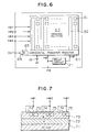
- FIG. 6 is a schematic diagram illustrating an embodiment of a CCD-type solid-state imaging apparatus using the charge transfer device of the present invention as a horizontal transfer register.
- an imaging section 63 comprises a plurality of photoelectric transducers 61 disposed in a matrix form in the vertical and horizontal directions for accumulating signal charges according to the quantity of incident light; and a plurality of vertical transfer registers 62 each disposed adjacent to a vertical array of photoelectric transducers 61, for vertically transferring the signal charges read from the corresponding array of photoelectric transducers 61.
- the photoelectric transducers 61 are formed of, for example, P-N junction photodiodes, while the vertical transfer registers 62 are comprised of CCDs.
- the signal charges accumulated in the photoelectric transducers 61 are read to the corresponding vertical transfer registers 62 via readout gates (not shown).
- the vertical transfer registers 62 are driven to transfer the signal charges by, for example, four-phase vertical transfer clocks V ⁇ 1 through V ⁇ 4.
- the signal charges read out to the vertical transfer registers 62 are sequentially transferred in the vertical direction by an amount of signal charges corresponding to one scanning line during part of the horizontal blanking period.
- Disposed below the imaging section 63 as viewed in Fig. 6 is a horizontal transfer register 64 for sequentially transferring signal charges by an amount associated with one line from the plurality of vertical transfer registers 62.
- This horizontal transfer register 64 is also formed of a CCD.
- the afore-described charge transfer device is used as the horizontal transfer register 64.
- the three groups (first, second and third) of gate electrodes 14, 15 and 16 are repeatedly disposed as transfer electrodes in an alternating sequence.
- a predetermined DC bias voltage is applied to the first group of gate electrodes 14 from the DC power supply 18, while the single-phase horizontal transfer clock H ⁇ fed from the exterior of the device is directly supplied to the third group of gate electrodes 16, and the horizontal transfer clock H ⁇ ' generated by delaying the clock H ⁇ in the delay circuit 21 by a predetermined delay time is supplied to the second group of gate electrodes 15.
- a charge detecting section 65 which is constructed of, for example, a floating diffusion amplifier, is disposed at the forward end of the horizontal transfer register 64 in the transfer direction.
- the horizontally-transferred signal charges are sequentially converted into signal voltages in the charge detecting section 65.
- the signal voltage is amplified in an output amplifier 66 and is then sent to the exterior of the device as an CCD output in accordance with the amount of incident light from a subject.
- the charge transfer device constructed in accordance with the present invention is employed as the horizontal transfer register 64 for use in the CCD solid-state imaging apparatus, thereby requiring only the single- phase horizontal transfer clock H ⁇ . Accordingly, this can decrease the number of terminals of the CCD solid-state imaging apparatus and also reduce power consumption, the heating amount and parasitic emissions. Additionally, the signal charge storage region can be enlarged to one third of the overall transfer length of the horizontal transfer register 64, thereby enabling an increase in the amount of charges to be handled.
- the charge transfer device of the present invention is applicable not only to a horizontal transfer register for use in a CCD solid-state imaging apparatus, but also to a charge transfer section in a CCD delay device or in a CCD linear sensor.
- the invention can be suitably used as a charge transfer section using a high-frequency transfer clock of 10 MHz or higher.
- Three groups of electrodes are repeatedly arranged in an alternating sequence above the transfer channel in the transfer direction.
- a predetermined bias voltage is applied to one group of electrodes, while a single-phase transfer clock provided from the exterior of the device and a transfer clock produced by delaying the single-phase transfer clock are supplied to the remaining two groups of electrodes.
- a single-phase transfer clock provided from the exterior of the device and a transfer clock produced by delaying the single-phase transfer clock are supplied to the remaining two groups of electrodes.
- the signal-charge storage region can be enlarged to one third of the overall transfer length, which is conventionally limited to one fourth of the overall transfer length of a known two-phase driving type of charge transfer device. This can increase the amount of charges to be handled.
Landscapes
- Physics & Mathematics (AREA)
- Engineering & Computer Science (AREA)
- Power Engineering (AREA)
- Electromagnetism (AREA)
- Condensed Matter Physics & Semiconductors (AREA)
- General Physics & Mathematics (AREA)
- Computer Hardware Design (AREA)
- Microelectronics & Electronic Packaging (AREA)
- Solid State Image Pick-Up Elements (AREA)
- Transforming Light Signals Into Electric Signals (AREA)
Applications Claiming Priority (2)
| Application Number | Priority Date | Filing Date | Title |
|---|---|---|---|
| JP1414/96 | 1996-01-09 | ||
| JP8001414A JPH09191101A (ja) | 1996-01-09 | 1996-01-09 | 電荷転送装置およびこれを用いた固体撮像装置 |
Publications (2)
| Publication Number | Publication Date |
|---|---|
| EP0784346A2 true EP0784346A2 (de) | 1997-07-16 |
| EP0784346A3 EP0784346A3 (de) | 1998-10-21 |
Family
ID=11500831
Family Applications (1)
| Application Number | Title | Priority Date | Filing Date |
|---|---|---|---|
| EP97400040A Withdrawn EP0784346A3 (de) | 1996-01-09 | 1997-01-09 | Ladungsübertragungsanordnung und Verwendung in einem Festkörperbildaufnahmegerät |
Country Status (4)
| Country | Link |
|---|---|
| US (1) | US5760430A (de) |
| EP (1) | EP0784346A3 (de) |
| JP (1) | JPH09191101A (de) |
| KR (1) | KR970060518A (de) |
Families Citing this family (7)
| Publication number | Priority date | Publication date | Assignee | Title |
|---|---|---|---|---|
| KR100259086B1 (ko) * | 1997-06-05 | 2000-06-15 | 김영환 | 고체촬상소자 및 이의 제조방법 |
| US6608647B1 (en) * | 1997-06-24 | 2003-08-19 | Cognex Corporation | Methods and apparatus for charge coupled device image acquisition with independent integration and readout |
| KR100332949B1 (ko) | 2000-05-23 | 2002-04-20 | 윤종용 | 전자 줌 기능에 적합한 고체 촬상 소자 |
| JP3804447B2 (ja) | 2000-12-20 | 2006-08-02 | セイコーエプソン株式会社 | 画像読み取り装置 |
| US20050029553A1 (en) * | 2003-08-04 | 2005-02-10 | Jaroslav Hynecek | Clocked barrier virtual phase charge coupled device image sensor |
| US7003068B2 (en) * | 2004-06-21 | 2006-02-21 | Kenet, Inc. | Device for subtracting or adding a constant amount of charge in a charge-coupled device at high operating frequencies |
| JP2020141029A (ja) * | 2019-02-27 | 2020-09-03 | 株式会社東芝 | 固体撮像装置 |
Family Cites Families (6)
| Publication number | Priority date | Publication date | Assignee | Title |
|---|---|---|---|---|
| US4047216A (en) * | 1974-04-03 | 1977-09-06 | Rockwell International Corporation | High speed low capacitance charge coupled device in silicon-sapphire |
| NL7709916A (nl) * | 1977-09-09 | 1979-03-13 | Philips Nv | Ladingsgekoppelde inrichting. |
| JPS5453830A (en) * | 1977-10-06 | 1979-04-27 | Toshiba Corp | Solide image pickup device |
| US4610019A (en) * | 1984-10-24 | 1986-09-02 | The United States Of America As Represented By The Secretary Of The Air Force | Energizing arrangement for charge coupled device control electrodes |
| JPH04373274A (ja) * | 1991-06-21 | 1992-12-25 | Sony Corp | Ccd固体撮像素子 |
| JPH06314706A (ja) * | 1993-04-30 | 1994-11-08 | Nec Corp | 電荷転送装置、その駆動方法およびその製造方法 |
-
1996
- 1996-01-09 JP JP8001414A patent/JPH09191101A/ja active Pending
- 1996-12-10 KR KR1019960063792A patent/KR970060518A/ko not_active Application Discontinuation
-
1997
- 1997-01-07 US US08/779,889 patent/US5760430A/en not_active Expired - Fee Related
- 1997-01-09 EP EP97400040A patent/EP0784346A3/de not_active Withdrawn
Non-Patent Citations (1)
| Title |
|---|
| None |
Also Published As
| Publication number | Publication date |
|---|---|
| EP0784346A3 (de) | 1998-10-21 |
| KR970060518A (ko) | 1997-08-12 |
| US5760430A (en) | 1998-06-02 |
| JPH09191101A (ja) | 1997-07-22 |
Similar Documents
| Publication | Publication Date | Title |
|---|---|---|
| US4774586A (en) | Interline type charge transfer imaging device | |
| EP0313322B1 (de) | Halbleiterbildsensor mit mehrfachen horizontalen Transferabschnitten | |
| US4750042A (en) | Solid state image pickup element with dual horizontal transfer sections | |
| US5040071A (en) | Image sensor having multiple horizontal shift registers | |
| US6445414B1 (en) | Solid-state image pickup device having vertical overflow drain and resistive gate charge transfer device and method of controlling thereof | |
| US4794279A (en) | A solid state imaging device which applies two separate storage voltages for the signal charges so as to reduce the smear level and the dark current | |
| US5757427A (en) | Image pick-up apparatus having a charge coupled device with multiple electrodes, a buffer layer located below some of the electrodes | |
| KR930002818B1 (ko) | Ccd 영상소자 | |
| KR900005875B1 (ko) | 고체 촬성 소자 | |
| US20040109075A1 (en) | CCD image sensor | |
| EP0663763B1 (de) | CCD-Bildsensor mit verringerter Übersprechung zwischen Photodioden | |
| US5760430A (en) | Charge transfer device and solid-state imaging apparatus using the same device | |
| US6034366A (en) | Color linear CCD image device and driving method | |
| US5589698A (en) | Solid state imaging device having sliding potential gradient | |
| US7184083B2 (en) | Solid state image pickup apparatus of low power consumption and its driving method | |
| JPS60119182A (ja) | 固体撮像素子 | |
| US4721989A (en) | CCD with transfer channel at lower potential than supply channel | |
| US20050173736A1 (en) | Solid-state imaging apparatus and charge transfer apparatus | |
| JP2820019B2 (ja) | 固体撮像素子 | |
| JPH0681280B2 (ja) | 電荷結合素子の駆動法 | |
| JP3677932B2 (ja) | 電荷転送装置およびこれを用いた固体撮像装置 | |
| JP2907841B2 (ja) | ラインセンサ | |
| JPS60244068A (ja) | 埋込みチヤネル電荷結合素子 | |
| JPH06326928A (ja) | 固体撮像装置および固体撮像装置の駆動方法 | |
| KR0151181B1 (ko) | 씨씨디 영상소자의 구조 |
Legal Events
| Date | Code | Title | Description |
|---|---|---|---|
| PUAI | Public reference made under article 153(3) epc to a published international application that has entered the european phase |
Free format text: ORIGINAL CODE: 0009012 |
|
| AK | Designated contracting states |
Kind code of ref document: A2 Designated state(s): DE FR GB |
|
| PUAL | Search report despatched |
Free format text: ORIGINAL CODE: 0009013 |
|
| AK | Designated contracting states |
Kind code of ref document: A3 Designated state(s): DE FR GB |
|
| 17P | Request for examination filed |
Effective date: 19990408 |
|
| RAP1 | Party data changed (applicant data changed or rights of an application transferred) |
Owner name: SONY CORPORATION |
|
| STAA | Information on the status of an ep patent application or granted ep patent |
Free format text: STATUS: THE APPLICATION IS DEEMED TO BE WITHDRAWN |
|
| 18D | Application deemed to be withdrawn |
Effective date: 20030909 |