EP0777290A1 - Nichtreziproke Doppelband-Schaltungsanordnung mit zwei nichtreziproken Schaltungselementen zum Betrieb in unterschiedlichen Frequenzbändern - Google Patents
Nichtreziproke Doppelband-Schaltungsanordnung mit zwei nichtreziproken Schaltungselementen zum Betrieb in unterschiedlichen Frequenzbändern Download PDFInfo
- Publication number
- EP0777290A1 EP0777290A1 EP96118934A EP96118934A EP0777290A1 EP 0777290 A1 EP0777290 A1 EP 0777290A1 EP 96118934 A EP96118934 A EP 96118934A EP 96118934 A EP96118934 A EP 96118934A EP 0777290 A1 EP0777290 A1 EP 0777290A1
- Authority
- EP
- European Patent Office
- Prior art keywords
- nonreversible circuit
- nonreversible
- plate
- dual
- ground conductor
- Prior art date
- Legal status (The legal status is an assumption and is not a legal conclusion. Google has not performed a legal analysis and makes no representation as to the accuracy of the status listed.)
- Withdrawn
Links
- 239000004020 conductor Substances 0.000 claims abstract description 75
- 229910000859 α-Fe Inorganic materials 0.000 claims abstract description 40
- 230000004907 flux Effects 0.000 claims description 4
- 239000007769 metal material Substances 0.000 description 6
- 238000007747 plating Methods 0.000 description 5
- 238000005476 soldering Methods 0.000 description 5
- PXHVJJICTQNCMI-UHFFFAOYSA-N Nickel Chemical compound [Ni] PXHVJJICTQNCMI-UHFFFAOYSA-N 0.000 description 4
- 230000005540 biological transmission Effects 0.000 description 3
- RYGMFSIKBFXOCR-UHFFFAOYSA-N Copper Chemical compound [Cu] RYGMFSIKBFXOCR-UHFFFAOYSA-N 0.000 description 2
- XEEYBQQBJWHFJM-UHFFFAOYSA-N Iron Chemical compound [Fe] XEEYBQQBJWHFJM-UHFFFAOYSA-N 0.000 description 2
- 229910052802 copper Inorganic materials 0.000 description 2
- 239000010949 copper Substances 0.000 description 2
- -1 for example Substances 0.000 description 2
- 238000004519 manufacturing process Methods 0.000 description 2
- 239000002184 metal Substances 0.000 description 2
- 229910052751 metal Inorganic materials 0.000 description 2
- 229910052759 nickel Inorganic materials 0.000 description 2
- 238000005516 engineering process Methods 0.000 description 1
- 229910052742 iron Inorganic materials 0.000 description 1
- 125000006850 spacer group Chemical group 0.000 description 1
Images


Classifications
-
- H—ELECTRICITY
- H01—ELECTRIC ELEMENTS
- H01P—WAVEGUIDES; RESONATORS, LINES, OR OTHER DEVICES OF THE WAVEGUIDE TYPE
- H01P1/00—Auxiliary devices
- H01P1/32—Non-reciprocal transmission devices
- H01P1/38—Circulators
- H01P1/383—Junction circulators, e.g. Y-circulators
- H01P1/387—Strip line circulators
Definitions
- This invention relates to a nonreversible circuit device for use in a terminal unit for transmission and reception in a radio communication system and, in particular, to a dual-band nonreversible circuit device operable in two different frequency bands specific to two different radio communication systems.
- the terminal unit typically includes a transmitter-receiver branching circuit for connecting a reception amplifier and a transmission amplifier to a common antenna and for isolating them from each other.
- the transmitter-receiver branching circuit generally includes those components relatively large in size.
- the transmitter-receiver branching circuit comprises a nonreversible circuit device.
- a nonreversible circuit device there is known a distributed-constant nonreversible circuit device comprising a magnet for generating a magnetic field, a set of center conductors, each serving as a signal path, a ferrite plate for providing the signal path with a unidirectional characteristic, and a ground conductor plate.
- An improved nonreversible circuit device comprising two sets of center conductors arranged in a single magnetic circuit is disclosed, for example, in Japanese Unexamined Patent Publications Nos. 58-85609 (85609/1983) (Reference 1) and 4-345201 (345201/1992) (Reference 2).
- the two sets of center conductors are connected in cascade with each other in one-to-one correspondence and grounded in the single magnetic circuit so as to increase an inductance without increasing the size of the device.
- a small-sized high-performance nonreversible circuit device is obtained.
- the two sets of center conductors are connected in parallel with each other in one-to-one correspondence and grounded in the single magnetic circuit so as to decrease an inductance component and a d.c. resistance in a high-frequency region without increasing the size of the device.
- a small-sized nonreversible circuit device excellent in high-frequency characteristic is obtained.
- the single terminal unit includes two transmitter-receiver branching circuits corresponding to the different frequencies.
- each of the transmitter-receiver branching circuits includes those components relatively large in size as described in the foregoing. As a result, the terminal unit inevitably becomes bulky as a whole.
- the terminal unit is desired to be small in size and light in weight even in case where the terminal unit is used in common in the two different radio communication systems.
- the nonreversible circuit device described in each of References 1 and 2 is operable at the single operation frequency. Therefore, for use in the two different radio communication systems of the two different frequencies, the terminal unit must include two nonreversible circuit devices corresponding to the two different frequencies. Thus, the nonreversible circuit device described in each of References 1 and 2 can not contribute to the reduction in size and weight of the terminal unit.
- a dual-band nonreversible circuit device comprising two nonreversible circuit elements contained in a single housing.
- Each of the two nonreversible circuit elements comprises a ferrite plate, a set of center conductors, a magnet, and a ground electrode.
- the housing provides a magnetic circuit for a magnetic flux from the magnet to provide a magnetic field within the housing.
- the two nonreversible circuit elements are operable for different frequency bands within the single magnetic housing.
- the dual-band nonreversible circuit device according to this invention is reduced in size and weight by adopting one of the following characteristics.
- the two nonreversible circuit elements operating within the single magnetic housing use a single ground electrode in common.
- the ground electrode forms a boundary between the two nonreversible circuit elements.
- the two nonreversible circuit elements operating within the single magnetic housing use a single magnet in common.
- the magnet forms a boundary between the two nonreversible circuit elements.
- each of the nonreversible circuit elements is a circulator element or an isolator element.
- Each of the preferred embodiments is directed to a dual-band circulator device comprising two circulator elements arranged in a single housing to be operable at different frequencies.
- a dual-band circulator device according to a first embodiment will be described.
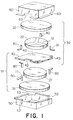
- first and second ferrite plates 21 and 22 and first and second center conductors 11 and 12 used in the dual-band circulator device according to this embodiment.
- the first ferrite plate 21 of a disk shape has a primary surface (lower surface in Fig. 1) provided with the first center conductor 11 and a secondary surface (upper surface in Fig. 1) opposite to the primary surface.
- the first center conductor 11 is formed on the primary surface by plating to radially outwardly extend from the center of the primary surface in three directions angularly spaced by 120°.
- the first center conductor 11 is extended onto a side surface of the first ferrite plate 21 to form extended ends.
- the secondary surface of the first ferrite plate 21 is subjected to plating, for example, nickel plating, in order to facilitate soldering as will later be described.
- the second ferrite plate 22 has a primary surface (upper surface in Fig. 1) provided with the second center conductor 12 and a secondary surface (lower surface in Fig. 1) subjected to plating.
- the second center conductor 12 has extended ends to be connected to input/output terminals 81 which will later be described.
- the dual-band circulator device has a structure which will presently be described.
- a first permanent magnet 31 is stacked on a lower magnetic yoke 50 having notches 53.
- the first ferrite plate 21 is superposed so that the primary surface having the first center conductor 11 is brought into contact with the first permanent magnet 31.
- a ground conductor plate 40 having notches 43 is stacked on the first ferrite plate 21 so that the secondary surface of the first ferrite plate 21 is brought into contact with one surface of the ground conductor plate 40, namely, a lower surface in Fig. 1.
- the secondary surface of the first ferrite plate 21 is fixed by soldering to the lower surface of the ground conductor plate 40.
- the second ferrite plate 22 is stacked so that the secondary surface of the second ferrite plate 22 is brought into contact with the other surface of the ground conductor plate 40, namely, an upper surface in Fig. 1.
- the secondary surface of the second ferrite plate 22 is fixed by soldering to the upper surface of the ground conductor plate 40.
- a second permanent magnet 32 is superposed so that the primary surface having the second center conductor 12 is brought into contact with the second permanent magnet 32.
- an upper magnetic yoke 60 having notches 63 is stacked.
- a combination of the lower and the upper magnetic yokes 50 and 60 serves as a single housing which encloses the first permanent magnet 31, the first ferrite plate 21 with the first center conductor 11, the ground conductor plate 40, the second ferrite plate 22 with the second center conductor 12, and the second permanent magnet 32.
- Each of the lower and the upper magnetic yokes 50 and 60 is made of a magnetic metal material so as to form a magnetic circuit for the magnetic flux from the first and the second permanent magnets 31 and 32 to thereby form a magnetic field within the single housing.
- the ground conductor plate 40 is made of a nonmagnetic metal material, for example, copper.
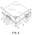
- the ground conductor plate 40 is held between opening edges of the lower and the upper magnetic yokes 50 and 60 and is fixedly supported thereby.
- the input/output terminals 80 and 81 of metal are connected to the extended ends of the first and the second center conductors 11 and 12, respectively.
- the input/output terminals 80 and 81 outwardly protrude through the notches 53 and 63 of the lower and the upper magnetic yokes 50 and 60, respectively.
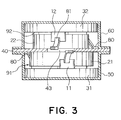
- a combination of the first permanent magnet 31, the first ferrite plate 21, the first center conductor 11, and the ground conductor plate 40 forms a first circulator element 91.
- a combination of the second permanent magnet 32, the second ferrite plate 22, the second center conductor 12, and the ground conductor plate 40 forms a second circulator element 92.
- the first and the second circulator elements 91 and 92 are designed to be operable in different frequency bands having center frequencies f A and f B , respectively.
- the dual-band circulator device according to this embodiment can be mounted in an area equal to that required for a single circulator device.
- the two circulator elements use the single ground conductor plate in common.
- the dual-band circulator device is reduced in height as compared with a simple stack of two separate circulator devices including two ground conductor plates.
- the number of parts is reduced so that the production cost is saved as compared with manufacture of two circulator devices including two ground conductor plates.
- the magnetic field is generated by the two permanent magnets, namely, the first and the second permanent magnets 31 and 32. It is noted here that the two permanent magnets can be replaced by a single permanent magnet as far as a magnetic field of a required level is generated. In this structure, however, either one of the first and the second center conductors 11 and 12 is brought into direct contact with a corresponding one of the lower and the upper magnetic yokes 50 and 60. Such direct contact must be avoided in any appropriate manner, for example, by the use of a spacer.
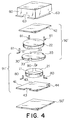
- the dual-band circulator device in this embodiment is similar in structure to the first embodiment except that the first and the second permanent magnets 31 and 32 are replaced by a single permanent magnet 30 and that the ground conductor plate 40 is replaced by first and second ground conductor plates 41 and 42. Similar parts are designated by like reference numerals.
- the first ground conductor plate 41 having notches 44 is stacked on a lower magnetic yoke 50'.
- the first ferrite plate 21 is superposed so that the secondary surface of the first ferrite plate 21 is brought into contact with the first ground conductor plate 41.
- the secondary surface of the first ferrite plate 21 is fixed by soldering to the first ground conductor plate 41.
- a permanent magnet 30 having notches 33 is stacked so that the primary surface of the first ferrite plate 21 with the first center conductor 11 is brought into contact with one surface of the permanent magnet 30, namely, a lower surface in Fig. 4.
- the second ferrite plate 22 is superposed so that the primary surface with the second center conductor 12 is brought into contact with the permanent magnet 30.
- the second ground conductor plate 42 is stacked so that the secondary surface of the second ferrite plate 22 is brought into contact with the second ground conductor plate 42.
- the secondary surface of the second ferrite plate 22 is fixed by soldering to the second ground conductor plate 42.
- the upper magnetic yoke 60 having the notches 63 is stacked.
- a combination of the lower and the upper magnetic yokes 50' and 60 serves as a single housing which encloses the first ground conductor plate 41, the first ferrite plate 21 with the first center conductor 11, the permanent magnet 30, the second ferrite plate 22 with the second center conductor 12, and the second ground conductor plate 42.
- Each of the lower and the upper magnetic yokes 50' and 60 is made of a magnetic metal material so as to form a magnetic circuit for the magnetic flux of the permanent magnet 30.
- each of the first and the second ground conductor plates 41 and 42 is made of a nonmagnetic metal material, for example, copper.
- the lower and the upper magnetic yokes 50' and 60 hold and support the first ground conductor plate 41 therebetween.
- the input/output terminals 80 of metal are connected to the extended ends of the first center conductor 11.
- the input/output terminals 81 are connected to the extended ends of the second center conductor 12.
- the input/output terminals 80 and 81 outwardly protrude through the notches 63 of the upper magnetic yoke 60.
- the input/output terminals 81 connected to the second center conductor 12 are longer than the input/output terminals 80 connected to the first center conductor 11 so as to outwardly protrude through the notches 63 of the upper magnetic yoke 60.
- a combination of the permanent magnet 30, the first ferrite plate 21, the first center conductor 11, and the first ground conductor plate 41 forms a first circulator element 91'.
- a combination of the permanent magnet 30, the second ferrite plate 22, the second center conductor 12, and the second ground conductor plate 42 forms a second circulator element 92'.
- the first and the second circulator elements 91' and 92' are designed to be operable in different frequency bands having different center frequencies.
- the dual-band circulator device of the above-mentioned structure has advantages similar to those described in conjunction with the first embodiment.
- each of the first and the second ground conductor plates 41 and 42 is made of a nonmagnetic metal material. If the first ground conductor plate 41 is made of a magnetic metal material, the first ground conductor plate 41 also serves as the lower magnetic yoke 50'. This makes it possible to further reduce the number of parts.
- the first ground conductor plate 41 may comprise an iron plate subjected to nickel plating for surface protection.
- each of the nonreversible circuit elements is not restricted to the distributed-constant circulator element described in the first and the second embodiments and may be any other appropriate element such as a lumped-constant circulator element.
- Each of the ground conductor plates may comprise a printed board with a ground electrode patterned thereon.
- the input/output terminals may be implemented by any other appropriate structure. For example, use is made of a surface-mounting structure in which an input/output electrode is separately patterned on the printed circuit board.
- the dual-band circulator device in which both of the two nonreversible circuit elements are the circulator elements.
- the circulator element acts as an isolator element if one terminal of the circulator element is terminated to a non-reflective resistance. In this manner, at least one of the two circulator elements of the dual-band circulator device may be transformed into the isolator element.
Landscapes
- Non-Reversible Transmitting Devices (AREA)
Applications Claiming Priority (2)
| Application Number | Priority Date | Filing Date | Title |
|---|---|---|---|
| JP7308650A JPH09148805A (ja) | 1995-11-28 | 1995-11-28 | デュアルバンド非可逆回路装置 |
| JP308650/95 | 1995-11-28 |
Publications (1)
| Publication Number | Publication Date |
|---|---|
| EP0777290A1 true EP0777290A1 (de) | 1997-06-04 |
Family
ID=17983630
Family Applications (1)
| Application Number | Title | Priority Date | Filing Date |
|---|---|---|---|
| EP96118934A Withdrawn EP0777290A1 (de) | 1995-11-28 | 1996-11-26 | Nichtreziproke Doppelband-Schaltungsanordnung mit zwei nichtreziproken Schaltungselementen zum Betrieb in unterschiedlichen Frequenzbändern |
Country Status (3)
| Country | Link |
|---|---|
| US (1) | US5898346A (de) |
| EP (1) | EP0777290A1 (de) |
| JP (1) | JPH09148805A (de) |
Cited By (1)
| Publication number | Priority date | Publication date | Assignee | Title |
|---|---|---|---|---|
| EP1041664A1 (de) * | 1999-03-30 | 2000-10-04 | Tokin Corporation | Nichtreziproke Doppelband-Schaltungsanordnung |
Families Citing this family (13)
| Publication number | Priority date | Publication date | Assignee | Title |
|---|---|---|---|---|
| JP3509762B2 (ja) * | 2001-02-16 | 2004-03-22 | 株式会社村田製作所 | 非可逆回路素子及び通信装置 |
| SE0101042D0 (sv) * | 2001-03-23 | 2001-03-23 | Ericsson Telefon Ab L M | Circulator and network |
| US7002426B2 (en) * | 2003-03-06 | 2006-02-21 | M/A-Com, Inc. | Above resonance isolator/circulator and method of manufacture thereof |
| US20040174224A1 (en) * | 2003-03-06 | 2004-09-09 | James Kingston | Above resonance Isolator/circulator and method of manufacture thereof |
| JP2004343273A (ja) | 2003-05-14 | 2004-12-02 | Alps Electric Co Ltd | 非可逆回路素子 |
| US9136572B2 (en) | 2013-07-26 | 2015-09-15 | Raytheon Company | Dual stripline tile circulator utilizing thick film post-fired substrate stacking |
| KR101601113B1 (ko) * | 2014-08-26 | 2016-03-08 | 홍익대학교 산학협력단 | 비가역 회로 소자 |
| US9899717B2 (en) | 2015-10-13 | 2018-02-20 | Raytheon Company | Stacked low loss stripline circulator |
| JP6705472B2 (ja) * | 2018-06-18 | 2020-06-03 | Tdk株式会社 | 非可逆回路素子及びこれを用いた通信装置 |
| JP6900963B2 (ja) | 2019-03-15 | 2021-07-14 | Tdk株式会社 | 非可逆回路素子及びこれを用いた通信装置 |
| US12418085B2 (en) | 2021-10-21 | 2025-09-16 | Ttm Technologies, Inc. | Circulator design and methods of fabricating the circulator |
| CN118826760B (zh) * | 2024-07-19 | 2025-12-19 | 人天通信集团有限公司 | 多频带通信系统及多频带通信系统构建方法 |
| CN118676566A (zh) * | 2024-07-19 | 2024-09-20 | 人天通信集团有限公司 | 具有双工作频带的铁氧体环形器 |
Citations (7)
| Publication number | Priority date | Publication date | Assignee | Title |
|---|---|---|---|---|
| FR2019690A1 (de) * | 1968-10-02 | 1970-07-03 | Japan Broadcasting Corp | |
| GB1254764A (en) * | 1968-04-02 | 1971-11-24 | Sits Soc It Telecom Siemens | Microwave four-port ferrite circulator |
| US3890582A (en) * | 1973-06-15 | 1975-06-17 | Addington Lab Inc | Floating-ground microwave ferrite isolators |
| JPS5885609A (ja) | 1981-11-18 | 1983-05-23 | Hitachi Metals Ltd | 集中定数型サ−キユレ−タおよびアイソレ−タ |
| JPH0255406A (ja) * | 1988-08-20 | 1990-02-23 | Fujitsu Ltd | サーキュレーター体型ハイブリッド |
| JPH04345201A (ja) | 1991-05-22 | 1992-12-01 | Tdk Corp | 非可逆回路素子用中心導体及び非可逆回路素子 |
| US5185587A (en) * | 1991-06-17 | 1993-02-09 | Renaissance Electronics Corp. | Compact tandem non-reciprocal circuit |
Family Cites Families (3)
| Publication number | Priority date | Publication date | Assignee | Title |
|---|---|---|---|---|
| US3781704A (en) * | 1972-03-30 | 1973-12-25 | Cutler Hammer Inc | High isolation circulator arrangement for low noise reflection type amplifiers |
| US5662754A (en) * | 1992-08-05 | 1997-09-02 | Murata Manufacturing Co., Ltd. | Method of making a high frequency non-reciprocal circuit element |
| JP3239959B2 (ja) * | 1992-08-05 | 2001-12-17 | 株式会社村田製作所 | マイクロ波用非可逆回路素子 |
-
1995
- 1995-11-28 JP JP7308650A patent/JPH09148805A/ja active Pending
-
1996
- 1996-11-26 EP EP96118934A patent/EP0777290A1/de not_active Withdrawn
- 1996-11-26 US US08/756,035 patent/US5898346A/en not_active Expired - Fee Related
Patent Citations (7)
| Publication number | Priority date | Publication date | Assignee | Title |
|---|---|---|---|---|
| GB1254764A (en) * | 1968-04-02 | 1971-11-24 | Sits Soc It Telecom Siemens | Microwave four-port ferrite circulator |
| FR2019690A1 (de) * | 1968-10-02 | 1970-07-03 | Japan Broadcasting Corp | |
| US3890582A (en) * | 1973-06-15 | 1975-06-17 | Addington Lab Inc | Floating-ground microwave ferrite isolators |
| JPS5885609A (ja) | 1981-11-18 | 1983-05-23 | Hitachi Metals Ltd | 集中定数型サ−キユレ−タおよびアイソレ−タ |
| JPH0255406A (ja) * | 1988-08-20 | 1990-02-23 | Fujitsu Ltd | サーキュレーター体型ハイブリッド |
| JPH04345201A (ja) | 1991-05-22 | 1992-12-01 | Tdk Corp | 非可逆回路素子用中心導体及び非可逆回路素子 |
| US5185587A (en) * | 1991-06-17 | 1993-02-09 | Renaissance Electronics Corp. | Compact tandem non-reciprocal circuit |
Non-Patent Citations (1)
| Title |
|---|
| PATENT ABSTRACTS OF JAPAN vol. 14, no. 222 (E - 0926) 10 May 1990 (1990-05-10) * |
Cited By (1)
| Publication number | Priority date | Publication date | Assignee | Title |
|---|---|---|---|---|
| EP1041664A1 (de) * | 1999-03-30 | 2000-10-04 | Tokin Corporation | Nichtreziproke Doppelband-Schaltungsanordnung |
Also Published As
| Publication number | Publication date |
|---|---|
| JPH09148805A (ja) | 1997-06-06 |
| US5898346A (en) | 1999-04-27 |
Similar Documents
| Publication | Publication Date | Title |
|---|---|---|
| US5898346A (en) | Dual-band nonreversible circuit device comprising two nonreversible circuit elements contained in a single housing to be operable in different frequency bands | |
| JP3417370B2 (ja) | 非可逆回路素子及び通信機装置 | |
| US6222425B1 (en) | Nonreciprocal circuit device with a dielectric film between the magnet and substrate | |
| EP0733274A1 (de) | Koaxialverbinder mit impedanzsteuerung | |
| KR980012700A (ko) | 비가역 회로 소자 | |
| EP0682380B1 (de) | Nichtreziprokes Schaltungselement | |
| KR100470311B1 (ko) | 비가역 회로 소자 및 통신장치 | |
| US6522216B2 (en) | Nonreciprocal circuit device and communication apparatus | |
| JP3539351B2 (ja) | 非可逆回路素子の製造方法 | |
| US6531930B2 (en) | Non-reciprocal circuit element having a grounding land between input/output patterns | |
| US6535074B2 (en) | Non-reciprocal circuit element, lumped element type isolator, and mobile communication unit | |
| JPH11239009A (ja) | 非可逆回路素子の広帯域化構造 | |
| JPH1065467A (ja) | フィルタ付き低雑音増幅器 | |
| JP2001094311A (ja) | 非可逆回路素子及び通信機装置 | |
| JP3125918B2 (ja) | アイソレータ | |
| JP4085364B2 (ja) | 非可逆回路素子 | |
| US6573809B1 (en) | Dielectric resonator device, dielectric duplexer, and communication apparatus incorporating same | |
| JPH06204912A (ja) | 送受信端回路装置 | |
| JPH1197911A (ja) | 集中定数型非可逆回路素子 | |
| JP3891437B2 (ja) | 3端子対非可逆素子及びこれを用いた通信装置 | |
| JPH11308013A (ja) | 集中定数型非可逆回路素子 | |
| JP4066333B2 (ja) | 非可逆回路素子 | |
| JPH07212107A (ja) | 非可逆回路素子 | |
| JPH08274511A (ja) | 集中定数型サーキュレータとその使用方法 | |
| JP2003060409A (ja) | ブルートゥース用rfモジュール |
Legal Events
| Date | Code | Title | Description |
|---|---|---|---|
| PUAI | Public reference made under article 153(3) epc to a published international application that has entered the european phase |
Free format text: ORIGINAL CODE: 0009012 |
|
| AK | Designated contracting states |
Kind code of ref document: A1 Designated state(s): DE FR GB |
|
| 17P | Request for examination filed |
Effective date: 19971021 |
|
| 17Q | First examination report despatched |
Effective date: 19980210 |
|
| STAA | Information on the status of an ep patent application or granted ep patent |
Free format text: STATUS: THE APPLICATION IS DEEMED TO BE WITHDRAWN |
|
| 18D | Application deemed to be withdrawn |
Effective date: 19980623 |