EP0773589A2 - Ebene Farbfilteranordnung für CCDs aus Farbstoffen und Beizmittelschichten - Google Patents
Ebene Farbfilteranordnung für CCDs aus Farbstoffen und Beizmittelschichten Download PDFInfo
- Publication number
- EP0773589A2 EP0773589A2 EP96203000A EP96203000A EP0773589A2 EP 0773589 A2 EP0773589 A2 EP 0773589A2 EP 96203000 A EP96203000 A EP 96203000A EP 96203000 A EP96203000 A EP 96203000A EP 0773589 A2 EP0773589 A2 EP 0773589A2
- Authority
- EP
- European Patent Office
- Prior art keywords
- color filter
- filter elements
- layer
- elements
- protective film
- Prior art date
- Legal status (The legal status is an assumption and is not a legal conclusion. Google has not performed a legal analysis and makes no representation as to the accuracy of the status listed.)
- Withdrawn
Links
- 239000000975 dye Substances 0.000 title description 45
- 239000000758 substrate Substances 0.000 claims abstract description 28
- 239000004065 semiconductor Substances 0.000 claims abstract description 27
- 239000000463 material Substances 0.000 claims abstract description 24
- 238000004519 manufacturing process Methods 0.000 claims abstract description 20
- 230000001681 protective effect Effects 0.000 claims description 47
- 238000000034 method Methods 0.000 claims description 39
- 238000005498 polishing Methods 0.000 claims description 32
- 239000000126 substance Substances 0.000 claims description 31
- 238000009792 diffusion process Methods 0.000 claims description 22
- 230000004888 barrier function Effects 0.000 claims description 20
- 238000000151 deposition Methods 0.000 claims description 20
- 239000007787 solid Substances 0.000 claims description 13
- 238000000059 patterning Methods 0.000 claims description 12
- 238000005530 etching Methods 0.000 claims description 9
- 238000001228 spectrum Methods 0.000 claims description 2
- 239000010410 layer Substances 0.000 description 148
- 229920002120 photoresistant polymer Polymers 0.000 description 25
- 239000011241 protective layer Substances 0.000 description 17
- 230000003595 spectral effect Effects 0.000 description 14
- 239000004642 Polyimide Substances 0.000 description 13
- 229920001721 polyimide Polymers 0.000 description 13
- 238000003491 array Methods 0.000 description 10
- 150000004767 nitrides Chemical class 0.000 description 10
- 230000005540 biological transmission Effects 0.000 description 9
- 238000004043 dyeing Methods 0.000 description 8
- 239000000049 pigment Substances 0.000 description 8
- 238000001429 visible spectrum Methods 0.000 description 8
- 238000000576 coating method Methods 0.000 description 7
- 239000011248 coating agent Substances 0.000 description 6
- 239000003086 colorant Substances 0.000 description 6
- 230000008020 evaporation Effects 0.000 description 6
- 238000001704 evaporation Methods 0.000 description 6
- 238000001020 plasma etching Methods 0.000 description 6
- 230000003287 optical effect Effects 0.000 description 5
- 239000002002 slurry Substances 0.000 description 5
- VYPSYNLAJGMNEJ-UHFFFAOYSA-N Silicium dioxide Chemical compound O=[Si]=O VYPSYNLAJGMNEJ-UHFFFAOYSA-N 0.000 description 4
- 239000002356 single layer Substances 0.000 description 4
- QVGXLLKOCUKJST-UHFFFAOYSA-N atomic oxygen Chemical compound [O] QVGXLLKOCUKJST-UHFFFAOYSA-N 0.000 description 3
- 210000004027 cell Anatomy 0.000 description 3
- 238000001312 dry etching Methods 0.000 description 3
- 230000000694 effects Effects 0.000 description 3
- TWNQGVIAIRXVLR-UHFFFAOYSA-N oxo(oxoalumanyloxy)alumane Chemical compound O=[Al]O[Al]=O TWNQGVIAIRXVLR-UHFFFAOYSA-N 0.000 description 3
- 239000001301 oxygen Substances 0.000 description 3
- 229910052760 oxygen Inorganic materials 0.000 description 3
- 229920000642 polymer Polymers 0.000 description 3
- 238000012876 topography Methods 0.000 description 3
- YCKRFDGAMUMZLT-UHFFFAOYSA-N Fluorine atom Chemical compound [F] YCKRFDGAMUMZLT-UHFFFAOYSA-N 0.000 description 2
- 229910052782 aluminium Inorganic materials 0.000 description 2
- 230000008021 deposition Effects 0.000 description 2
- 229910052731 fluorine Inorganic materials 0.000 description 2
- 239000011737 fluorine Substances 0.000 description 2
- 239000011521 glass Substances 0.000 description 2
- 238000001459 lithography Methods 0.000 description 2
- 229910052751 metal Inorganic materials 0.000 description 2
- 239000002184 metal Substances 0.000 description 2
- 239000000377 silicon dioxide Substances 0.000 description 2
- 230000008961 swelling Effects 0.000 description 2
- 206010070834 Sensitisation Diseases 0.000 description 1
- RTAQQCXQSZGOHL-UHFFFAOYSA-N Titanium Chemical compound [Ti] RTAQQCXQSZGOHL-UHFFFAOYSA-N 0.000 description 1
- 229910052770 Uranium Inorganic materials 0.000 description 1
- XAGFODPZIPBFFR-UHFFFAOYSA-N aluminium Chemical compound [Al] XAGFODPZIPBFFR-UHFFFAOYSA-N 0.000 description 1
- 238000013459 approach Methods 0.000 description 1
- 239000008280 blood Substances 0.000 description 1
- 210000004369 blood Anatomy 0.000 description 1
- 210000002421 cell wall Anatomy 0.000 description 1
- 238000005229 chemical vapour deposition Methods 0.000 description 1
- 230000000295 complement effect Effects 0.000 description 1
- 238000004049 embossing Methods 0.000 description 1
- 238000011049 filling Methods 0.000 description 1
- 239000012530 fluid Substances 0.000 description 1
- 239000007789 gas Substances 0.000 description 1
- 150000002500 ions Chemical class 0.000 description 1
- 230000001788 irregular Effects 0.000 description 1
- 238000002955 isolation Methods 0.000 description 1
- 239000007788 liquid Substances 0.000 description 1
- 150000002739 metals Chemical class 0.000 description 1
- 238000002156 mixing Methods 0.000 description 1
- 239000000203 mixture Substances 0.000 description 1
- 239000000178 monomer Substances 0.000 description 1
- 239000011368 organic material Substances 0.000 description 1
- 238000000206 photolithography Methods 0.000 description 1
- 239000002861 polymer material Substances 0.000 description 1
- 238000004886 process control Methods 0.000 description 1
- 229920006395 saturated elastomer Polymers 0.000 description 1
- 230000008313 sensitization Effects 0.000 description 1
- 229910021332 silicide Inorganic materials 0.000 description 1
- 125000006850 spacer group Chemical group 0.000 description 1
- 238000004544 sputter deposition Methods 0.000 description 1
- 229910052715 tantalum Inorganic materials 0.000 description 1
- GUVRBAGPIYLISA-UHFFFAOYSA-N tantalum atom Chemical compound [Ta] GUVRBAGPIYLISA-UHFFFAOYSA-N 0.000 description 1
- 239000010936 titanium Substances 0.000 description 1
- 229910052719 titanium Inorganic materials 0.000 description 1
- WFKWXMTUELFFGS-UHFFFAOYSA-N tungsten Chemical compound [W] WFKWXMTUELFFGS-UHFFFAOYSA-N 0.000 description 1
- 229910052721 tungsten Inorganic materials 0.000 description 1
- 239000010937 tungsten Substances 0.000 description 1
Images


Classifications
-
- H—ELECTRICITY
- H10—SEMICONDUCTOR DEVICES; ELECTRIC SOLID-STATE DEVICES NOT OTHERWISE PROVIDED FOR
- H10F—INORGANIC SEMICONDUCTOR DEVICES SENSITIVE TO INFRARED RADIATION, LIGHT, ELECTROMAGNETIC RADIATION OF SHORTER WAVELENGTH OR CORPUSCULAR RADIATION
- H10F39/00—Integrated devices, or assemblies of multiple devices, comprising at least one element covered by group H10F30/00, e.g. radiation detectors comprising photodiode arrays
- H10F39/011—Manufacture or treatment of image sensors covered by group H10F39/12
- H10F39/024—Manufacture or treatment of image sensors covered by group H10F39/12 of coatings or optical elements
-
- H—ELECTRICITY
- H10—SEMICONDUCTOR DEVICES; ELECTRIC SOLID-STATE DEVICES NOT OTHERWISE PROVIDED FOR
- H10F—INORGANIC SEMICONDUCTOR DEVICES SENSITIVE TO INFRARED RADIATION, LIGHT, ELECTROMAGNETIC RADIATION OF SHORTER WAVELENGTH OR CORPUSCULAR RADIATION
- H10F77/00—Constructional details of devices covered by this subclass
- H10F77/30—Coatings
- H10F77/306—Coatings for devices having potential barriers
- H10F77/331—Coatings for devices having potential barriers for filtering or shielding light, e.g. multicolour filters for photodetectors
-
- H—ELECTRICITY
- H10—SEMICONDUCTOR DEVICES; ELECTRIC SOLID-STATE DEVICES NOT OTHERWISE PROVIDED FOR
- H10F—INORGANIC SEMICONDUCTOR DEVICES SENSITIVE TO INFRARED RADIATION, LIGHT, ELECTROMAGNETIC RADIATION OF SHORTER WAVELENGTH OR CORPUSCULAR RADIATION
- H10F39/00—Integrated devices, or assemblies of multiple devices, comprising at least one element covered by group H10F30/00, e.g. radiation detectors comprising photodiode arrays
- H10F39/80—Constructional details of image sensors
- H10F39/805—Coatings
- H10F39/8053—Colour filters
Definitions
- This invention relates to a solid state color image sensor which include a plurality of color filter elements.
- a solid state imager can be viewed as including a number of laterally offset pixels containing photosensitive regions.
- Arrays of color filter elements transmitting selected portions of the visible spectrum and placed in registration with the pixels of a solid state imager are well known to the art and can take a variety of forms.
- Each color filter element transmits a portion of the color spectrum of incident light into the associated pixel of the imager in order to provide the imager with means of color sensitization.
- All visible image sensors including linear sensors, can utilize color filters whether or not the photosensitive region occupies the entire pixel area.
- the color filter elements are transmissive of a set of primary colors such as red, green and blue or of complementary colors such as cyan, yellow, and magenta and or white.
- Lens arrays integral to the image sensor commonly made by thermal deformation of photolithographically defined polymers, are often employed over color filter arrays to direct light rays through color filter elements to the photosensitive regions.
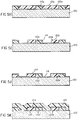
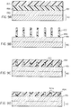
- Fig. 1 shows a single pixel 10 of a typical interline image sensor in registration with color filter elements 24a and 24b partially including a color filter array, lens 22, photodiode 14 formed in semiconductor substrate 12, gate electrode 16, and light shield 18.
- the gate electrode and light shield are typically isolated electrically from one another and from the substrate by isolation oxides not shown.
- a color filter array includes a plurality of color filter elements 24a, 24b, and 24c, typically provided in a pattern of three or more elements each transmitting a different spectral region.
- Photodiode 14, semiconductor substrate 12, gate electrode 16, and light shield 18 form semiconductor portion 40 of the imager.
- the prior art image sensor with a pixel shown in Fig. 1 has a partially planarizing layer 20a for offsetting the color filter element 24a from photodiodes 14.
- the partially planarizing layer includes an organic spacer layer spin coated to achieve some degree of planarization in order to provide simpler processing conditions for deposition of the color filter array, such as the color filter arrays described in Nomura, U.S. Pat. No. 5,321,249, typically coated from organic materials.
- Partially planarizing layer 20a enables better process control of the thickness of the color filter elements, essential in controlling the spectral transmission characteristics.
- the use and limitations of such planarizing layers in optically active solid state image sensors is taught by McColgin, U.S. Pat. No. 4,553,153 for a polymerizable monomer.
- Upper planarizing layer 20b in Fig. 1 is typically used to space lens 22 away from photodiode 14 and partially compensates for irregular topography of conventional color filter elements.
- prior art color filter arrays suffer to some degree from lack of planarity, due to both lack of planarity of the substrate on which they are formed (region 60 of Fig. 1 and of Fig. 2A and 2B) and lack of planarity of the color filter elements relative to one another (region 62 of Fig. 1 and of Fig. 2A and 2B).
- Lack of planarity of the substrate produces variations in the thickness of the color filter element materials coated on the substrates, which in turn causes local differences in the optical transmission characteristics within each element.
- Lack of planarity between color filter elements region 62 of Fig. 1 and of Fig.
- 4,387,146 disclose the confinement of dyes in cells, but the means of fabrication using organic cell structures with thick cell walls formed photolithographically or by embossing has not proven advantageous for small pixel imagers due to the gap between dyed regions, and to the fact that thin walls are prone to distortion when they are not supported by material between them, as is the case for the cells described U.S. Pat. No. 4,387,146 and U.S. Pat. No. 4,307,165. This is particularly true for semiconductor process environments due to the use of fluid baths whose surface tension can distort unsupported thin walls, as is well known in the art.
- an image sensor which includes an integral color filter array, comprising:
- an image sensor which includes an integral color filter array, comprising:
- An advantage of image sensors made in accordance with this invention is that the gap between color filter elements is minimal or vanishes entirely. It is also advantageous that there can be no overlap between color filter elements.
- color filter elements may be self aligned to one another so that mask to mask misalignments do not degrade performance or yield.
- An advantage of this invention is that the surface upon which the color filter array is disposed is rendered optically planar so that light rays are refracted only as expected from an ideal dielectric interface.
- a further advantage is that substantially identical processes may be used to make arrays from a variety of materials.
- a feature of image sensors made in accordance with this invention is that the top surface of the color filter array is entirely planar.
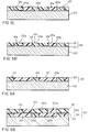
- support layer 100 preferably a spin on glass, is provided over semiconductor portion 40 of an imager, the imager being depicted in Fig. 1. Where like parts correspond, the same numbers are used in these and the remaining figures.
- the thickness of support layer 100 is preferably greater than the height of the topography of semiconductor portion 40, typically between 0.5 and 1.0 micron.
- support layer 100 is rendered optically planar by chemical mechanical polishing, such that incident light rays on surface 101 of support layer 100 are refracted only as expected at an ideal planar dielectric interface.
- Fig. 3A support layer 100, preferably a spin on glass, is provided over semiconductor portion 40 of an imager, the imager being depicted in Fig. 1. Where like parts correspond, the same numbers are used in these and the remaining figures.
- the thickness of support layer 100 is preferably greater than the height of the topography of semiconductor portion 40, typically between 0.5 and 1.0 micron.
- support layer 100 is rendered optically planar by chemical mechanical polishing, such that incident light rays on surface 101 of support
- a first color filter layer 110 with planar surface 111 preferably a dyed polyimide or a pigment or a pigment mixture, is provided uniformly on planar surface 101 of support layer 100.
- First color filter layer 110 may be spin coated, in the preferred case that it is a dyed polyimide, or may be deposited by other means, such as evaporation, in the case that the it is an evaporable pigment.
- first protective film 114 preferably an etch stop to chemical mechanical polishing such as a nitride film of thickness from 100 A to 1000 A, is deposited uniformly on planar surface 101.
- first etching first protective layer 114 and the second etching first color filter layer 110 is used to define first color filter elements 110a with planar surfaces 111a, as shown in Fig. 3D.
- a second color filter layer 120 preferably also a dyed polyimide transmitting a different portion of the visible spectrum from that of first color filter layer 110, is shown deposited with a thickness exceeding that of first color filter layer 110, as depicted in Fig. 3E.
- second color filter layer 120 may be spin coated in the preferred case that it is a dyed polyimide, or it may be deposited by other means, such as evaporation, in the case that the color filter layer is an evaporable pigment. This layer is then removed, preferably by chemical mechanical polishing, using a slurry of aluminum oxide entirely from, over the first color filter elements 110a, thereby forming adjacent second color filter elements 120a (Fig. 3F).
- planar surfaces 121a of second color filter elements 120a are shown substantially coplanar with the surfaces 111a of the first color filter elements 110a. This may be accomplished by extending the time of chemical mechanical polishing slightly beyond that required for the removal of the second color filter layer from over the first color filter elements, while still retaining a planar surface 121a, as is well known in the art of chemical mechanical polishing.
- photoresist 122 is coated and patterned so that the photoresist openings in the photoresist extend from near the middle of second color filter element 120a to just over first color filter element 110a. Then, by using an etch which is selective to first protective layer 114 and to support layer 100, preferably an oxygen containing reactive ion etch, openings 128 (Fig. 3H) in the second color filter elements are provided with their edges self-aligned to first color filter elements 110a by means of protective layer 114. Second color filter elements 120a are thereby shortened to become modified second color filter elements 120b (Fig. 3H) with planar surfaces 121b.
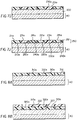
- a third color filter layer 130 also preferably a dyed polyimide transmitting a different portion of the visible spectrum from that of the first or second color filter elements 110a and 120b, with a thickness exceeding that of the coplanar first and second color filter elements.
- Third color filter layer 130 may be spin coated in the preferred case that it is a dyed polyimide, or it may be deposited by other means, such as evaporation, in the case that the color filter layer is an evaporable pigment.
- Color filter layer 130 is then removed, preferably by chemical mechanical polishing, using a slurry of aluminum oxide, entirely from over the first and modified second color filter elements 110a and 120b, thereby forming adjacent third color filter elements 130a with planar surfaces 131a (Fig. 3J). Also shown in Fig. 3J, the remaining portions of first protective layer 114 have been removed, by either dry etching in a fluorine containing atmosphere for the preferred case in which the first protective layer is nitride, or by further use of chemical mechanical polishing, thereby providing planar surfaces 111a, 121a, and 131a of contiguous color filter elements 110a, 120b, and 130a, all having sharply defined lateral boundaries without any regions of vertical overlap.
- Fig. 3G1-3J1 depict a related embodiment of the present invention which may be used to make three element color filter arrays in which two of the three colors do not share adjacent edges, as for the color filter pattern shown in plan view in Fig. 3J1.
- the green color filter element would be the typical choice for the color filter element 110a with planar surface 111a (Fig. 3J) comprising the largest portion of the array surface.
- Fig. 3G1 depicts the structure made in accordance with the previous embodiment (Fig. 3F and 3G) having two color filter elements 110a and 120a.
- Fig. 3F and 3G the structure made in accordance with the previous embodiment having two color filter elements 110a and 120a.
- an entire color filter element 120a is exposed by patterned photoresist 122 and removed by etching, preferably anisotropic reactive ion etching (Fig. 3H1). Then, using the method discussed in the previous embodiment, a third color filter element 130a is formed in the region from which the entire color filter element 120a was removed. In this manner, the color filter array shown in plan view in Fig. 3J1 is constructed in a minimal number of fabrication steps. It is advantageous in this application that the position of all color filter elements is determined solely by the edge locations of the first color filter element and not by subsequent mask to mask alignments.
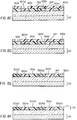
- a method is provided by which a color filter array 150 is made in two planar parts, an upper planar color filter array 156 and a lower planar color filter array 154 (Fig. 4E).
- this method is initially similar to that discussed in association with Fig. 3A to 3F, in which a support layer 100 is provided having planar surface 101 on which is provided first and second color filter elements 110a and 120a, identical to the structure of Fig. 3F.
- Fig. 4A this method is initially similar to that discussed in association with Fig. 3A to 3F, in which a support layer 100 is provided having planar surface 101 on which is provided first and second color filter elements 110a and 120a, identical to the structure of Fig. 3F.
- protective film 114 is shown removed, preferable by dry etching in a fluorine containing atmosphere for the preferred case in which the first protective layer is nitride, or by further use of chemical mechanical polishing, thereby providing planar surfaces 111a, 121a.
- the color filter layers may be spin coated in the preferred case that they are dyed polyimides, or may be deposited by other means, such as evaporation, in the case that they are evaporable pigments.
- a lower planar array surface 155 of lower color filter array 154 is formed, as depicted in Fig. 4A.
- FIG. 4A It is next desired to repeat the process described above (Fig. 4A) to establish an upper planar color filter array 156 with upper planar array surface 157 (Fig. 4E).
- this process is initiated by uniformly providing a second protective film 124, preferably an evaporated nitride, overlying upper planar array surface 151 and by then providing sequentially third color filter layer 130 and third protective layer 134, of materials similar to those discussed in the previous embodiments.
- Third color filter layer 130 and third protective layer 134 are patterned in a manner similar to first color filter layer 110 and first protective layer 114, using conventional photoresist and sequential reactive ion etching, to provide third color filter elements 130a (Fig. 4C) with planar surfaces 131 (Fig. 4C).
- a fourth color filter layer 140 preferably also a polyimide, is shown coated, at least to a thickness equal to that of third color filter element 130a, and planarized by chemical mechanical polishing to remove fourth color filter layer 140 from over third color filter elements 130a to provide fourth color filter elements 140a with top surfaces 141a.
- planarization preferably by dry etching or by chemical mechanical polishing using a silica based slurry, an upper planar array surface 157 is formed, free of third protective film 134, as depicted in Fig. 4E.
- a method of making a color filter array 150 from upper and lower planar color filter arrays 154 and 156 respectively in registration with one another and with the photosensitive regions 14 (Fig. 3A) of imager semiconductor portion 40.
- a choice of spectral characteristics of the overlying color filter elements for example cyan for one layer and magenta for the overlying layer, results in various desired primary color transmissions, in this example blue.
- one of the four color filter elements in this embodiment is selected to be uncolored, serving only to provide a uniform optical index and mechanical planarity for color filter array 150.
- FIG. 5A-5C semiconductor portion 40, comprising photosensitive regions 14, electrodes 16, and lightshields 18 are shown as representative of the typical elements of semiconductor portion 40 of a solid state imager, on which it is desired to provide an integral, planar color filter array.
- this array is made by first providing a support layer 100 (Fig.
- support layer 100 is planarized optically flat, preferably by chemical mechanical polishing, so that light rays directed toward planar surface 101 are refracted as expected from an ideal planar dielectric surface.
- a first color filter layer 110 typically a dyed polyimide, with top surface 111, which transmits a selected portion of the visible spectrum of light incident on the imager.
- First color filter layer 110 may be spin coated in the preferred case that it is a dyed polyimide, or may be deposited by other means, such as evaporation, is the case that the color filter layer is an evaporable material such as a pigment.
- first color filter layer 110 is shown patterned by conventional photolithography using photoresist 112 and etching, preferably by reactive ion etching in an oxygen plasma, to form first color filter element 110a with surfaces 111a, located in registration with the photosensitive region 14 of the imager.
- first protective film 114 preferably a conformally sputtered dielectric film such as oxide or nitride, which covers the top and side surfaces of first color filter element 110a and exposed planar surface 101 which is both a dye diffusion barrier and which can serve additionally as a suitable etch stop for subsequent chemical mechanical polishing.
- a second color filter layer 120 preferably also a dyed polyimide but transmitting a different portion of the visible spectrum from that of first color filter layer 110, is shown deposited with a thickness exceeding that of the first color filter layer 110, as depicted in Fig. 5G.
- Second color filter layer 120 may be spin coated in the preferred case that it is a dyed polyimide, or may be deposited by other means, such as evaporation, in the case that the color filter layer is an evaporable pigment.
- This layer is then removed, preferably by chemical mechanical polishing, using a slurry of aluminum oxide, entirely from over the first color filter elements 110a, thereby forming adjacent second color filter elements 120a (Fig. 5H).
- the surfaces 121a of second color filter elements 120a are shown substantially coplanar with the surfaces 111a of the first color filter elements 110a. This may be accomplished by extending the time of polishing beyond that required for the removal of the second color filter layer over the first color filter elements, while still retaining a planar surface 121, as is well known in the art of chemical mechanical polishing.
- a third color filter element having a spectral transmission characteristic different from that of the other two color filter elements and located adjacent to the other color filter elements but separated form them by a dye diffusion barrier. This is preferable accomplished by etching away a portion of second color element 120a, for example by using a silylated photoresist patterned by conventional lithography and reactive ion etching in an oxygen plasma, thereby forming modified second color filter elements 120b with surfaces 121b (Fig. 5I).
- a second protective film 124 preferably also a conformally deposited nitride or oxide which is additionally a suitable etch stop for subsequent chemical mechanical polishing, is deposited on the exposed top and side surfaces of first and modified second color filter element 110a and 120b and exposed support layer surface 101, as shown in Fig. 5K.
- a third color filter layer 130 is provided (Fig. 5K) to a depth at least the height of the first color filter element 110a, and is removed from over the first and modified second color filter elements 110a and 120b respectively, forming third color filter elements 130a with planar surfaces 131a.
- the surfaces 131a are shown in Fig.
- a planar color filter array 150 with a planar array surface 151 free of protective films 114 and 124, is formed, as depicted in Fig. 5M.
- color filter elements 110a, 120b, and 130a may be obtained, since color filter element 110a has no underlying protective film, color filter element 120b has one underlying protective film (114) , and color filter element 130a has both underlying protective films (114 and 124).
- a planar color filter array is achieved comprised of an upper and lower planar color filter array as disclosed in the discussion of Fig. 4 but including the feature of a dye diffusion barrier separating each color filter element.
- a lower color filter array 154 is shown comprised of color filter elements 110a and 120a separated by protective film 114.
- an upper color filter array 156 is provided in registry with lower color filter array 154.
- a preferred embodiment is described in which the consecutive replacement of color filter elements is used to effect a single layer color filter array with color filter elements separated from one another by dye diffusion barriers and having an arbitrary number of color filter elements all self-aligned, independent of mask to mask alignment tolerances.
- a first color filter layer 210 preferably of a dyed polyimide or other dyed polymer material capable of being etched.
- First color filter layer 210 is shown patterned by conventional lithography, for example by the use of silylated photoresist, in Fig.
- first color filter elements 210a with planar surfaces 211a, in registry with alternate pixels of the underlying semiconductor portion (not shown).
- first protective film 214 preferably comprised of a transparent dielectric such as nitride or oxide.
- a second color filter layer 220 is shown coated and patterned to form second color filter elements 220a (Fig. 7B) with planar surfaces 221a, in a manner similar to that discussed in the previous embodiments.
- the materials of first and second color filter elements 210a and 220a are indicated to be identical, for the purpose of illustrating the nature of the present embodiment. In general, however, the two color filter elements could be chosen to have different spectral characteristics.
- photoresist 222 has been patterned with openings 228 defined within every third color filter element, regardless of the whether the color filter element is a first (210a) or second (220a) color filter element.
- Fig. 7G the color filter elements so selected by openings 228 in photoresist 222 have been removed, regardless of the whether the color filter element is a first or second color filter element.
- An overlap region 223 of photoresist 222 is shown in Fig. 7G and is permitted providing the etch used to remove the color filter elements in openings 228 is substantially selective against photoresist 222 as well as support layer 100.
- the choice of which of the color filter elements of Fig. 7E to replace is totally arbitrary, thereby affording substantial flexibility in the positioning and number of color filter elements desired in the color filter array.
- this method advantageously provides for an arbitrary number of color filter elements all self-aligned, independent of mask to mask alignment tolerances. It is also to be appreciated that although this example is shown in Fig.
- first and second color filter layers 210 and 220 are identical for simplicity of illustrating a final repeat pattern of three distinct color filter elements
- all other choices for the spectral characteristics of the color filter layers are in principal possible as well as the choices of which color filter elements are to be replaced, and such general choices may be desired for certain applications.
- the material chosen for the first two color filter layers may be a sacrificial material picked for other characteristics, such as its ability to be selectively etched, and therefore may be replaced by consequently repeating three times the sequence of steps leading to replacement of one color filter element with another described in Fig. 7F-Fig. 7H in this embodiment.
- Fig. 8A yet another preferred embodiment is described, in which the consecutive dying of mordant materials is used to effect a single layer color filter array with color filter elements separated from one another by dye diffusion barriers and having an arbitrary number of color filter elements all self-aligned independent of mask to mask alignment tolerances.
- This embodiment also advantageously prevents lateral diffusion of the color filter elements during dyeing of the mordant, otherwise a disadvantage of mordant dyeing.
- a structure is formed on a semiconductor portion (not shown) identical to that shown in Fig.
- first and second color filter elements 210a and 220a are replaced by first and second mordant elements 310a and 320a formed from first and second mordant layers 310 and 320, (not shown) by the same fabrication sequence described in association with Fig. 7A-7E.
- the mordant layers 310 and 320 are preferably polymeric materials capable of being dyed subsequently to form color filter elements whose spectral characteristics are determined by the type of dye.
- protective film 314, preferably nitride is formed in a manner identical to protective film 214 by the same fabrication sequence described in association with Fig. 7A-7E.
- photoresist 322 has been defined to provide openings well within every third mordant element, regardless of the whether the mordant element was a first or second mordant element.
- the photoresist is preferably chosen not to imbibe dye when dyeing is performed.
- the structure of Fig. 8B is dyed with a first dye type, for example by being placed in a liquid dye bath, thereby forming color filter elements 310a1 and 320a1, formed respectively from dyeing first and second mordant elements 310a and 320a.
- a first dye type for example by being placed in a liquid dye bath
- FIG. 8D and 8E patterning a photoresist so as to have openings inside every third mordant element and dyeing the thereby selected first and second mordant elements 310a and 320a
- Fig. 8D and 8E to form color filter elements 310a2 and 320a2, formed respectively from dyeing first and second mordant elements 310a and 320a with dye of a second type.
- the process is repeated a third time, as shown in Fig. 8F, to form color filter elements 310a3 and 320a3, formed respectively from dyeing first and second mordant elements 310a and 320a with dye of a third type.
- FIG. 9 another preferred embodiment is shown in which the consecutive dying of mordant materials is used as in the previous embodiment to effect a single layer color filter array with color filter elements separated from on another by dye diffusion barriers but in which the structure shown in Fig. 8A is achieved as shown in Fig. 9A, by first coating upper support layer 494, preferably nitride, on lower support layer 490, preferably oxide, with optically planar front surface 491 made planar by chemical mechanical polishing, then depositing photoresist 412. As in the other embodiments, semiconductive portion 40 underlies upper and lower support layers 494 and 490. Next, photoresist 412 is patterned (Fig.
- mordant layer 410 is fully removed from the remaining portions of upper support layer 494, but this is not always required in cases in which the mordant layer 410 is not too thick, for example less than 1000 ⁇ thick, in regions over the remaining portions of upper support layer 410.
- a structure is provided for the consecutive dying of mordant materials separated from on another by dye diffusion barriers by the steps of first coating and patterning a single mordant layer 410, Fig. 10A, on a support layer 400 and then patterning photoresist 412 with narrow openings (Fig. 10B) which allow the etching of grooves 415 through selected regions of single mordant layer 410.
- protective layer 414 preferably nitride, is deposited in groves 415 and on single mordant layer 410, as shown in Fig. 10C.
- protective layer 414 is removed from over single mordant layer 410 but not from groves 415, preferably by chemical mechanical polishing. Again, the resulting structure is of the form of Fig. 8A as is required to complete the fabrication of the type of color filter array described in association with Fig. 8A.
- Protective layer 414 may also be metallic, for example comprising a metal from the group tungsten, tantalum, and titanium and the silicides of these metals, and aluminum, to act as a light shield as well as a dye diffusion barrier.
- the invention in which at least one of the color filter elements does not substantially absorb light in the visible spectrum.
- the invention in which the surface of the support layer on the semiconductor substrate is optically planar.
- the invention in which at least one of the color filter elements does not substantially absorb light in the visible spectrum.
- the method further including the steps of:
- the method further including the steps of:
- a method of making a solid state image sensor having a color filter array with color filter elements separated by vertical diffusion barriers comprising:
- An image sensor which includes an integral color filter array comprising:
- a method of making a solid state image sensor color filter from dyeable mordant elements separated at all adjacent vertical sidewalls by a protective film which is a dye diffusion barrier comprising:
- a method of making a solid state image sensor color filter from dyeable mordant elements separated at all adjacent vertical sidewalls by a protective film which is a dye diffusion barrier comprising:
- a method of making a solid state image sensor color filter from dyeable mordant elements separated at all adjacent vertical sidewalls by a protective film which is a dye diffusion barrier comprising:
Landscapes
- Solid State Image Pick-Up Elements (AREA)
- Optical Filters (AREA)
- Color Television Image Signal Generators (AREA)
Applications Claiming Priority (2)
| Application Number | Priority Date | Filing Date | Title |
|---|---|---|---|
| US08/554,884 US5708264A (en) | 1995-11-07 | 1995-11-07 | Planar color filter array for CCDs from dyed and mordant layers |
| US554884 | 1995-11-07 |
Publications (2)
| Publication Number | Publication Date |
|---|---|
| EP0773589A2 true EP0773589A2 (de) | 1997-05-14 |
| EP0773589A3 EP0773589A3 (de) | 1997-07-02 |
Family
ID=24215093
Family Applications (1)
| Application Number | Title | Priority Date | Filing Date |
|---|---|---|---|
| EP96203000A Withdrawn EP0773589A3 (de) | 1995-11-07 | 1996-10-28 | Ebene Farbfilteranordnung für CCDs aus Farbstoffen und Beizmittelschichten |
Country Status (3)
| Country | Link |
|---|---|
| US (2) | US5708264A (de) |
| EP (1) | EP0773589A3 (de) |
| JP (1) | JPH09172153A (de) |
Cited By (3)
| Publication number | Priority date | Publication date | Assignee | Title |
|---|---|---|---|---|
| EP0965865A1 (de) * | 1998-05-20 | 1999-12-22 | Eastman Kodak Company | Nanopartikel in Farbfilter-Arrays |
| CN100419951C (zh) * | 2004-04-13 | 2008-09-17 | 台湾积体电路制造股份有限公司 | 形成半导体元件及半导体影像感测器的方法 |
| CN109065641A (zh) * | 2013-12-09 | 2018-12-21 | 太阳能公司 | 使用自对准注入和封盖制造太阳能电池发射极区 |
Families Citing this family (41)
| Publication number | Priority date | Publication date | Assignee | Title |
|---|---|---|---|---|
| JP3308778B2 (ja) * | 1995-09-29 | 2002-07-29 | 株式会社東芝 | 固体撮像装置の製造方法 |
| US5677202A (en) * | 1995-11-20 | 1997-10-14 | Eastman Kodak Company | Method for making planar color filter array for image sensors with embedded color filter arrays |
| US5798542A (en) * | 1996-10-08 | 1998-08-25 | Eastman Kodak Company | Image sensor having ITO electrodes with overlapping color filters for increased sensitivity |
| US5954559A (en) * | 1997-01-13 | 1999-09-21 | Image Quest Technologies, Inc. | Color filter structure and method of making |
| US6057586A (en) * | 1997-09-26 | 2000-05-02 | Intel Corporation | Method and apparatus for employing a light shield to modulate pixel color responsivity |
| US6297071B1 (en) * | 1998-07-22 | 2001-10-02 | Eastman Kodak Company | Method of making planar image sensor color filter arrays |
| US6456793B1 (en) | 2000-08-03 | 2002-09-24 | Eastman Kodak Company | Method and apparatus for a color scannerless range imaging system |
| US20020084407A1 (en) * | 2000-12-28 | 2002-07-04 | Xerox Corporation | Systems and methods for fabricating an electro-optical device used for image sensing |
| JP4092914B2 (ja) * | 2001-01-26 | 2008-05-28 | セイコーエプソン株式会社 | マスクの製造方法、有機エレクトロルミネッセンス装置の製造方法 |
| EP1430281A1 (de) * | 2001-09-11 | 2004-06-23 | LumiLeds Lighting U.S., LLC | Farbsensor |
| US7057654B2 (en) * | 2002-02-26 | 2006-06-06 | Eastman Kodak Company | Four color image sensing apparatus |
| US6800838B2 (en) * | 2002-10-25 | 2004-10-05 | Omnivision International Holding Ltd | Image sensor having reduced stress color filters and method of making |
| US6998207B2 (en) * | 2003-04-03 | 2006-02-14 | Taiwan Semiconductor Manufacturing Co., Ltd. | High performance color filter process for image sensor |
| US7502058B2 (en) * | 2003-06-09 | 2009-03-10 | Micron Technology, Inc. | Imager with tuned color filter |
| KR20050032438A (ko) * | 2003-10-01 | 2005-04-07 | 동부아남반도체 주식회사 | Cmos 이미지 센서 및 그 제조 방법 |
| US7385167B2 (en) * | 2004-07-19 | 2008-06-10 | Micron Technology, Inc. | CMOS front end process compatible low stress light shield |
| CN101095043A (zh) * | 2004-11-16 | 2007-12-26 | 数据色彩控股股份公司 | 设计有集成cie彩色匹配滤波器的比色计的方法 |
| WO2006055682A2 (en) * | 2004-11-17 | 2006-05-26 | Datacolor Holding Ag | Tristimulus colorimeter having integral dye filters |
| US7345764B2 (en) * | 2005-02-07 | 2008-03-18 | Vladimir Bulovic | Apparatus and method for a slim format spectrometer |
| KR100934513B1 (ko) * | 2005-02-10 | 2009-12-29 | 도판 인사츠 가부시키가이샤 | 고체 촬상 소자 및 그 제조 방법 |
| US7580130B2 (en) * | 2005-03-23 | 2009-08-25 | Datacolor Holding Ag | Method for designing a colorimeter having integral illuminant-weighted CIE color-matching filters |
| US7474402B2 (en) * | 2005-03-23 | 2009-01-06 | Datacolor Holding Ag | Reflectance sensor for integral illuminant-weighted CIE color matching filters |
| JP4905760B2 (ja) * | 2005-06-15 | 2012-03-28 | 富士フイルム株式会社 | カラーフィルタの製造方法、カラーフィルタ、固体撮像素子の製造方法およびこれを用いた固体撮像素子 |
| US7808023B2 (en) * | 2005-08-24 | 2010-10-05 | Aptina Imaging Corporation | Method and apparatus providing integrated color pixel with buried sub-wavelength gratings in solid state imagers |
| KR100720468B1 (ko) * | 2005-12-28 | 2007-05-22 | 동부일렉트로닉스 주식회사 | 씨모스 이미지 센서 및 그 제조방법 |
| JP4449936B2 (ja) * | 2006-03-31 | 2010-04-14 | ソニー株式会社 | 撮像装置、カメラシステムおよびその駆動方法 |
| US20070238035A1 (en) * | 2006-04-07 | 2007-10-11 | Micron Technology, Inc. | Method and apparatus defining a color filter array for an image sensor |
| US7799491B2 (en) * | 2006-04-07 | 2010-09-21 | Aptina Imaging Corp. | Color filter array and imaging device containing such color filter array and method of fabrication |
| JP2007294525A (ja) * | 2006-04-21 | 2007-11-08 | Fujifilm Corp | 固体撮像素子の製造方法 |
| KR100766248B1 (ko) * | 2006-07-12 | 2007-10-12 | 동부일렉트로닉스 주식회사 | 이미지 소자 및 이의 제조 방법 |
| US7410822B2 (en) * | 2006-07-20 | 2008-08-12 | United Microelectronics Corp. | Method for forming color filter |
| US8158307B2 (en) * | 2007-02-14 | 2012-04-17 | Fujifilm Corporation | Color filter and method of manufacturing the same, and solid-state image pickup element |
| US20080204580A1 (en) * | 2007-02-28 | 2008-08-28 | Micron Technology, Inc. | Method, apparatus and system providing imaging device with color filter array |
| US20090104545A1 (en) * | 2007-10-22 | 2009-04-23 | Visera Technologies Company Limited | Color filter and fabrication method thereof |
| JP2009198664A (ja) * | 2008-02-20 | 2009-09-03 | Fujifilm Corp | カラーフィルタ及びその製造方法並びに固体撮像素子 |
| CN101588506B (zh) * | 2008-05-22 | 2012-05-30 | 索尼株式会社 | 固体摄像装置及其制造方法以及电子设备 |
| JP4835719B2 (ja) | 2008-05-22 | 2011-12-14 | ソニー株式会社 | 固体撮像装置及び電子機器 |
| US20100208266A1 (en) * | 2009-02-17 | 2010-08-19 | Colman Shannon | Tristimulus colorimeter having integral dye filters |
| US20110119595A1 (en) * | 2009-11-19 | 2011-05-19 | Telegent Systems USA, Inc. | Apparatus and Method for Browser Based Integration of Broadcast Television and Internet Content |
| JP2012074521A (ja) * | 2010-09-28 | 2012-04-12 | Sony Corp | 固体撮像装置の製造方法、固体撮像装置、および電子機器 |
| US10103194B2 (en) * | 2016-09-26 | 2018-10-16 | Omnivision Technologies, Inc. | Self-aligned optical grid on image sensor |
Citations (11)
| Publication number | Priority date | Publication date | Assignee | Title |
|---|---|---|---|---|
| US4081277A (en) | 1976-10-08 | 1978-03-28 | Eastman Kodak Company | Method for making a solid-state color imaging device having an integral color filter and the device |
| US4204866A (en) | 1976-10-08 | 1980-05-27 | Eastman Kodak Company | Solid-state color imaging devices and method for making them |
| US4247799A (en) | 1978-01-30 | 1981-01-27 | Eastman Kodak Company | Color imaging devices and color filter arrays using photo-bleachable dyes |
| US4307165A (en) | 1980-10-02 | 1981-12-22 | Eastman Kodak Company | Plural imaging component microcellular arrays, processes for their fabrication, and electrographic compositions |
| JPS574012A (en) * | 1980-06-09 | 1982-01-09 | Canon Inc | Production of color filter |
| US4315978A (en) | 1980-03-06 | 1982-02-16 | Eastman Kodak Company | Solid-state color imaging device having a color filter array using a photocrosslinkable barrier |
| US4387146A (en) | 1980-09-08 | 1983-06-07 | Eastman Kodak Company | Multicolor filters with nonplanar support elements |
| US4553153A (en) | 1983-10-21 | 1985-11-12 | Eastman Kodak Company | Planarizing layer for semiconductor substrates such as solid state imagers |
| US4764670A (en) | 1986-06-20 | 1988-08-16 | Eastman Kodak Company | Color filter arrays |
| US4876167A (en) | 1987-08-20 | 1989-10-24 | Eastman Kodak Company | Color filter array containing a photocrosslinked polymeric mordant |
| US5321249A (en) | 1991-10-31 | 1994-06-14 | Matsushita Electric Industrial Co., Ltd. | Solid-state imaging device and method of manufacturing the same |
Family Cites Families (12)
| Publication number | Priority date | Publication date | Assignee | Title |
|---|---|---|---|---|
| JPS50147339A (de) * | 1974-05-16 | 1975-11-26 | ||
| JPS556342A (en) * | 1978-06-28 | 1980-01-17 | Fuji Photo Film Co Ltd | Production of multicolor optical filter |
| JPS5687782U (de) * | 1979-12-10 | 1981-07-14 | ||
| NL8103146A (nl) * | 1980-07-03 | 1982-02-01 | Dainippon Screen Mfg | Werkwijze voor het vervaardigen van streepzeven. |
| NL8105071A (nl) * | 1981-11-10 | 1983-06-01 | Philips Nv | Kleurenbeeldopneeminrichting. |
| JPS60247202A (ja) * | 1984-05-23 | 1985-12-06 | Seiko Epson Corp | カラ−フイルタ− |
| NL8700033A (nl) * | 1987-01-09 | 1988-08-01 | Philips Nv | Werkwijze voor het vervaardigen van een halfgeleiderinrichting van het type halfgeleider op isolator. |
| KR920013734A (ko) * | 1990-12-31 | 1992-07-29 | 김광호 | 칼라필터의 제조방법 |
| US5162251A (en) * | 1991-03-18 | 1992-11-10 | Hughes Danbury Optical Systems, Inc. | Method for making thinned charge-coupled devices |
| JP3092869B2 (ja) * | 1991-10-02 | 2000-09-25 | シャープ株式会社 | 多色表示装置の製造方法 |
| JP2863422B2 (ja) * | 1992-10-06 | 1999-03-03 | 松下電子工業株式会社 | 固体撮像装置およびその製造方法 |
| JPH06232379A (ja) * | 1993-02-01 | 1994-08-19 | Sharp Corp | 固体撮像素子 |
-
1995
- 1995-11-07 US US08/554,884 patent/US5708264A/en not_active Expired - Fee Related
-
1996
- 1996-10-28 EP EP96203000A patent/EP0773589A3/de not_active Withdrawn
- 1996-11-05 JP JP8292957A patent/JPH09172153A/ja active Pending
- 1996-12-10 US US08/763,029 patent/US5719074A/en not_active Expired - Fee Related
Patent Citations (11)
| Publication number | Priority date | Publication date | Assignee | Title |
|---|---|---|---|---|
| US4081277A (en) | 1976-10-08 | 1978-03-28 | Eastman Kodak Company | Method for making a solid-state color imaging device having an integral color filter and the device |
| US4204866A (en) | 1976-10-08 | 1980-05-27 | Eastman Kodak Company | Solid-state color imaging devices and method for making them |
| US4247799A (en) | 1978-01-30 | 1981-01-27 | Eastman Kodak Company | Color imaging devices and color filter arrays using photo-bleachable dyes |
| US4315978A (en) | 1980-03-06 | 1982-02-16 | Eastman Kodak Company | Solid-state color imaging device having a color filter array using a photocrosslinkable barrier |
| JPS574012A (en) * | 1980-06-09 | 1982-01-09 | Canon Inc | Production of color filter |
| US4387146A (en) | 1980-09-08 | 1983-06-07 | Eastman Kodak Company | Multicolor filters with nonplanar support elements |
| US4307165A (en) | 1980-10-02 | 1981-12-22 | Eastman Kodak Company | Plural imaging component microcellular arrays, processes for their fabrication, and electrographic compositions |
| US4553153A (en) | 1983-10-21 | 1985-11-12 | Eastman Kodak Company | Planarizing layer for semiconductor substrates such as solid state imagers |
| US4764670A (en) | 1986-06-20 | 1988-08-16 | Eastman Kodak Company | Color filter arrays |
| US4876167A (en) | 1987-08-20 | 1989-10-24 | Eastman Kodak Company | Color filter array containing a photocrosslinked polymeric mordant |
| US5321249A (en) | 1991-10-31 | 1994-06-14 | Matsushita Electric Industrial Co., Ltd. | Solid-state imaging device and method of manufacturing the same |
Non-Patent Citations (1)
| Title |
|---|
| PATENT ABSTRACTS OF JAPAN vol. 006, no. 062 (P - 111) 21 April 1982 (1982-04-21) * |
Cited By (4)
| Publication number | Priority date | Publication date | Assignee | Title |
|---|---|---|---|---|
| EP0965865A1 (de) * | 1998-05-20 | 1999-12-22 | Eastman Kodak Company | Nanopartikel in Farbfilter-Arrays |
| CN100419951C (zh) * | 2004-04-13 | 2008-09-17 | 台湾积体电路制造股份有限公司 | 形成半导体元件及半导体影像感测器的方法 |
| CN109065641A (zh) * | 2013-12-09 | 2018-12-21 | 太阳能公司 | 使用自对准注入和封盖制造太阳能电池发射极区 |
| CN109065641B (zh) * | 2013-12-09 | 2022-05-10 | 太阳能公司 | 使用自对准注入和封盖制造太阳能电池发射极区 |
Also Published As
| Publication number | Publication date |
|---|---|
| US5719074A (en) | 1998-02-17 |
| US5708264A (en) | 1998-01-13 |
| JPH09172153A (ja) | 1997-06-30 |
| EP0773589A3 (de) | 1997-07-02 |
Similar Documents
| Publication | Publication Date | Title |
|---|---|---|
| US5719074A (en) | Method of making a planar color filter array for CCDS from dyed and mordant layers | |
| US5677202A (en) | Method for making planar color filter array for image sensors with embedded color filter arrays | |
| US6297071B1 (en) | Method of making planar image sensor color filter arrays | |
| US5466926A (en) | Colored microlens array and method of manufacturing same | |
| US7989752B2 (en) | Solid-state imaging device and solid-state imaging device manufacturing method | |
| US5605783A (en) | Pattern transfer techniques for fabrication of lenslet arrays for solid state imagers | |
| US7566405B2 (en) | Micro-lenses for CMOS imagers and method for manufacturing micro-lenses | |
| US6211916B1 (en) | Solid state imager with inorganic lens array | |
| US5734190A (en) | Imager having a plurality of cylindrical lenses | |
| US20040080638A1 (en) | CMOS image sensor including photodiodes having different depth accordong to wavelength of light | |
| US5711890A (en) | Method for forming cylindrical lens arrays for solid state imager | |
| EP0124025A2 (de) | Festkörper-Farbbildaufnahmevorrichtung und Herstellungsverfahren | |
| US5824236A (en) | Method for forming inorganic lens array for solid state imager | |
| JP2609339B2 (ja) | カラ−フィルタ−の製造方法 | |
| US20050045805A1 (en) | Solid-state image sensor and a manufacturing method thereof | |
| JP4510613B2 (ja) | 固体撮像装置の製造方法 | |
| US5384231A (en) | Fabricating lens array structures for imaging devices | |
| JP2841037B2 (ja) | Ccd固体撮像素子の製造方法 | |
| JPH11317511A (ja) | 固体撮像装置の製造方法 | |
| CN100405607C (zh) | 具有用脊结构隔开的微透镜的图象传感器及其制造方法 | |
| KR20020052713A (ko) | 칼라필터어레이 형성 방법 | |
| JP2000012814A (ja) | オンチップレンズ付カラー固体撮像素子とその製造方法 | |
| KR20040083173A (ko) | 이미지 소자의 제조 방법 | |
| KR930003614B1 (ko) | 칼라필터의 제조방법 | |
| KR0166807B1 (ko) | 고체촬상 소자의 칼라필터 제조방법 |
Legal Events
| Date | Code | Title | Description |
|---|---|---|---|
| PUAI | Public reference made under article 153(3) epc to a published international application that has entered the european phase |
Free format text: ORIGINAL CODE: 0009012 |
|
| AK | Designated contracting states |
Kind code of ref document: A2 Designated state(s): DE FR GB |
|
| PUAL | Search report despatched |
Free format text: ORIGINAL CODE: 0009013 |
|
| AK | Designated contracting states |
Kind code of ref document: A3 Designated state(s): DE FR GB |
|
| 17P | Request for examination filed |
Effective date: 19971231 |
|
| 17Q | First examination report despatched |
Effective date: 20021128 |
|
| STAA | Information on the status of an ep patent application or granted ep patent |
Free format text: STATUS: THE APPLICATION IS DEEMED TO BE WITHDRAWN |
|
| 18D | Application deemed to be withdrawn |
Effective date: 20030409 |