EP0772225B1 - Filtre a energie electronique - Google Patents
Filtre a energie electronique Download PDFInfo
- Publication number
- EP0772225B1 EP0772225B1 EP95925121A EP95925121A EP0772225B1 EP 0772225 B1 EP0772225 B1 EP 0772225B1 EP 95925121 A EP95925121 A EP 95925121A EP 95925121 A EP95925121 A EP 95925121A EP 0772225 B1 EP0772225 B1 EP 0772225B1
- Authority
- EP
- European Patent Office
- Prior art keywords
- magnetic field
- deflecting
- electrons
- incident
- radius
- Prior art date
- Legal status (The legal status is an assumption and is not a legal conclusion. Google has not performed a legal analysis and makes no representation as to the accuracy of the status listed.)
- Expired - Lifetime
Links
Images


Classifications
-
- H—ELECTRICITY
- H01—ELECTRIC ELEMENTS
- H01J—ELECTRIC DISCHARGE TUBES OR DISCHARGE LAMPS
- H01J37/00—Discharge tubes with provision for introducing objects or material to be exposed to the discharge, e.g. for the purpose of examination or processing thereof
- H01J37/02—Details
- H01J37/04—Arrangements of electrodes and associated parts for generating or controlling the discharge, e.g. electron-optical arrangement, ion-optical arrangement
- H01J37/05—Electron or ion-optical arrangements for separating electrons or ions according to their energy or mass
-
- H—ELECTRICITY
- H01—ELECTRIC ELEMENTS
- H01J—ELECTRIC DISCHARGE TUBES OR DISCHARGE LAMPS
- H01J49/00—Particle spectrometers or separator tubes
- H01J49/44—Energy spectrometers, e.g. alpha-, beta-spectrometers
-
- H—ELECTRICITY
- H01—ELECTRIC ELEMENTS
- H01J—ELECTRIC DISCHARGE TUBES OR DISCHARGE LAMPS
- H01J49/00—Particle spectrometers or separator tubes
- H01J49/44—Energy spectrometers, e.g. alpha-, beta-spectrometers
- H01J49/46—Static spectrometers
-
- H—ELECTRICITY
- H01—ELECTRIC ELEMENTS
- H01J—ELECTRIC DISCHARGE TUBES OR DISCHARGE LAMPS
- H01J49/00—Particle spectrometers or separator tubes
- H01J49/44—Energy spectrometers, e.g. alpha-, beta-spectrometers
- H01J49/46—Static spectrometers
- H01J49/48—Static spectrometers using electrostatic analysers, e.g. cylindrical sector, Wien filter
-
- H—ELECTRICITY
- H01—ELECTRIC ELEMENTS
- H01J—ELECTRIC DISCHARGE TUBES OR DISCHARGE LAMPS
- H01J2237/00—Discharge tubes exposing object to beam, e.g. for analysis treatment, etching, imaging
- H01J2237/05—Arrangements for energy or mass analysis
- H01J2237/055—Arrangements for energy or mass analysis magnetic
-
- H—ELECTRICITY
- H01—ELECTRIC ELEMENTS
- H01J—ELECTRIC DISCHARGE TUBES OR DISCHARGE LAMPS
- H01J2237/00—Discharge tubes exposing object to beam, e.g. for analysis treatment, etching, imaging
- H01J2237/05—Arrangements for energy or mass analysis
- H01J2237/057—Energy or mass filtering
-
- H—ELECTRICITY
- H01—ELECTRIC ELEMENTS
- H01J—ELECTRIC DISCHARGE TUBES OR DISCHARGE LAMPS
- H01J2237/00—Discharge tubes exposing object to beam, e.g. for analysis treatment, etching, imaging
- H01J2237/26—Electron or ion microscopes
- H01J2237/28—Scanning microscopes
- H01J2237/2802—Transmission microscopes
Definitions
- the present invention relates to an electronic energy filter which is arranged to separate only electrons having specific energy from an electron beam and form an image of those electrons.
- the electrons transmitted through a specimen suffer from energy loss that is peculiar to one or more elements composing the specimen.
- the electrons transmitted through the specimen are passed through an energy filter for analyzing energy of those electrons, separating only the electrons suffering from the specific energy loss, and forming an image of the separated electrons.
- the formed image corresponds to a mapping image of one or more specific elements contained in the specimen.
- the use of only the electrons having specific energy for forming an image allows the energy loss of the electrons caused by the thickness of the specimen to be restricted to only specific electrons.
- the resulting image has excellent contrast.
- the omega type energy filter is composed of three electromagnets as shown in Fig. 2.
- the first electromagnet 1 has an opposite deflecting direction to the second and the third electromagnets 2 and 3.
- Incident electrons 4 are traced like an omega ( ⁇ ) and are fired in the same direction as the incident one, for selecting only the electrons having specific energy loss.
- a numeral 5 denotes a crossover point.
- a numeral 6 denotes an inlet image surface.
- a numeral 7 denotes an outlet image surface.
- a numeral 8 denotes an energy dispersion surface.
- the alpha type energy filter is composed of three electromagnets 11, 12 and 13 having the same deflecting direction, as shown in Fig. 3.
- Incident electrons 4 are traced like an alpha ( ⁇ ) and finally outgoes in the same direction as the incident one, for selecting only the electrons that suffer from specific energy loss.
- Another kind of alpha type energy filter is shown in Fig. 4 (Perez, J.P., Sirven, J., Sequela, A., and Lacaze, J.C., Journal de Physique, (Paris), 45, Coll. Cs, 171 to 174 (1984)).
- This energy filter is constructed so that an electromagnet 14 having a deflecting angle of 70° is located as opposed to the other electromagnet 15 having a deflecting angle of 220° with narrow middle space 16, in which those electromagnets yield the corresponding magnetic field intensities.
- an incident electron beam 4 goes around the inside of the filter for analyzing the energy of the electron beam.
- the electron energy filter is required to form an energy dispersion surface and an image surface with a small aberration. That is, the electrons 4 transmitted through the specimen enter at the crossover point 5 formed on a lens into the electron energy filter, pass through the filter and reach the energy dispersion surface 8 where the electrons having the specific energy are converged in the same direction though the electrons having the other energy are dispersed. On the energy dispersion surface 8, hence, the aberration has to be eliminated in order to restrict a lower resolution of the electrons passing through a slit. Moreover, the image formed on an inlet image surface 6 before the electron energy filter is required to be similarly formed on an outlet image surface point 7. Hence, the aberration has to be reduced to a minimum for suppressing the distortion of the image as much as possible.
- a convergence condition of the electron optical system provided in the electron energy filter arranged to use a fanlike electromagnet may be calculated by using a calculation program of an ion optical system used for designing a mass spectrometer.
- the convergence characteristic up to a three degrees, which considers the effect of an end magnetic field, can be precisely calculated by the calculation program TRIO that is completed by Matuo, Matuda, et al. (T. Matsuo, H. Matusda, Y. Fujita and H. Wollnik; Mass Spectroscopy, Vol. 24, No.1, March 1976)
- the electron optical system of the aforementioned conventional electron energy filter does not make sufficient allowance for the effect of the end magnetic field.
- the image point formed after the passage of the electrons through the electron energy filter is required to make the energy dispersion disappear, converge the image in two directions, and have the magnifications of the images kept at a value of 1.
- the electron optical system does not completely meet these conditions.
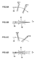
- the y-directional convergence is given by the oblique passage of charged particles in the inlet and the outlet end magnetic fields of the fanlike magnetic field. That is, when the angles formed between the vertical plane to the electron beam 30 and the ends of the electromagnets 31 and 32 have the relations of EP11 and EP12 as shown in Fig. 5A (where the angles EP11 and EP12 have positive signs), the electron beam 30 is converted in the y direction as shown in Fig. 5B.
- the angles formed between the vertical plane to the electron beam 30 and the ends of the electromagnets 31 and 32 have the relations of EP21 and EP22 as shown in Fig. 5C (where the angles EP21 and EP22 have negative signs), the electron beam 30 is dispersed in the y direction as shown in Fig. 5D.
- the distortion and the aberration of the image may be reduced to a minimum.
- the secondary aberration may be represented as follows.
- x 2 Xx 1 + A ⁇ 1 + D ⁇ 1 + XXx 1 2 + XAx 1 ⁇ 1 + AA ⁇ 1 2 + XDx 1 ⁇ 1 + AD ⁇ 1 ⁇ 1 + DD ⁇ 1 2 + YYy 1 2 + YBy 1 ⁇ 1 + BB ⁇ 1 2
- y 2 Yy 1 + B ⁇ 1 + YXy 1 x 1 + YAy 1 ⁇ 1 + YDy 1 ⁇ 1 + BX ⁇ 1 x 1 + BA ⁇ 1 ⁇ 1 + BD ⁇ 1 ⁇ 1
- x is a beam width in the direction of the energy dispersion caused by the fanlike magnetic field
- a is a spread angle
- ⁇ is a spread of energy
- y is a beam width that is vertical to x
- ⁇ is a spread angle in the y-direction.
- a subscript 1 represents an initial condition of the beam.
- a subscript 2 represents a beam width of a converged image.
- X, A, D, Y and B represent a first-order aberration coefficient.
- XX, XA, AA and the like represent a secondary aberration coefficient.
- the resulting energy filter does not offer excellent performance.
- the secondary aberration coefficients XD, AD, DD, YD and BD about the energy width ⁇ may be negligible, because the energy width ⁇ 1 of the electrons are allowed to be restricted to 10 -4 or lower through the slit. Since the other beam spread is as wide as 10 -3 , it is necessary to design the electron optical system so that the secondary aberration coefficient may be made far smaller.
- the table 1 lists the values of the aberration coefficients calculated by the TRIO in the electron optical systems of the omega type energy filter shown in Fig. 2 and the alpha type energy filter shown in Figs. 3 and 4.
- the form parameters of each energy filter required for the calculation are derived from Optik 73, No. 3 (1986)99-107.
- the aberration is a value of ⁇ m if the beam spread is in the order of 10 -3 . If the aberration at an image point is 100 ⁇ m, the image expanded to be 100 times larger through the projecting lens system of the electron microscope has a distortion of 1 cm, which is not an excellent filtered image.
- the alpha type energy filter such as Perez offers an image point where the secondary aberration is 5 mm, the first-order magnification Y in the y direction is 28, and the y-directional aberration coefficient B is 3. Hence, the resulting image is not converged and extremely distorted.
- the further problems the prior art involves are reduction of magnetic poles in number and compact design, which is due to location of the filter on the way of a mirror body.
- the conventional systems rather than the alpha type energy filter of Perez, et al. with a large image distortion need four magnetic poles and thus as many end magnetic fields for the incident and outgoing electron beam as eight. The end magnetic fields may make the beam convergence uncertain.
- JP-A-61-2 977 Another document which discloses electron energy filters having either two or four magnetic field regions to achieve an ⁇ -shaped electron beam path is JP-A-61-2 977.
- the filters with only two magnetic field regions disclosed in this document have these regions arranged closely adjacent each other. There does not exist an entire space between the regions where there would be no field.
- Other electron energy filters having either one or three magnetic field regions to achieve ⁇ - or ⁇ -shaped electron beam paths are disclosed in JP-A-61-277 141.
- Claim 16 relates to a transmission electron microscope having an electron energy filter of the invention.
- the deflecting angle WM1 of the first magnetic field is shifted largely from 90°, the area of the magnetic pole is made larger, so the compact design of the filter is not allowed.
- WM1 and WM2 are substantially 90° and 180°, respectively, the electron beams in the free space are kept in parallel.
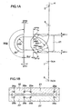
- Fig. 1 is a schematic view showing the magnetic poles of an electron energy filter according to an embodiment of the present invention, in which Fig. 1A is a plane view and Fig. 1B is a central section.
- An electron beam 4 is deflected through the effect of a first magnetic field generated between a pair of magnetic poles 21 and 21' by virtue of current flowing through coils 25a and 25b and a second magnetic field generated between a pair of magnetic poles 22 and 22' by virtue of current flowing through coils 26a and 26b.
- the deflected beam 4 travels straight on a first path and enters into the second magnetic field yielded by the second pair of magnetic poles 22 and 22', in which the beam is deflected 180° in the substantially same direction. Then, the beam travels on the second path in the free space, which is substantially parallel to the first path, and then-is again incident to the first magnetic field in which the beam is deflected 90° with the same radius as the first deflection. Hence, the beam is rotated totally 360° and then outgoes in the same direction as the incident one.
- the trace radius AM2 of the electron beam in the second magnetic field is about half as long as the track radius AM1 in the first magnetic field, for reducing the magnetic poles 21 and 22 in area.
- the electron beam is traced as a gamma ( ⁇ ).
- the y-directional convergence effect is brought about by the oblique outgoing and re-incident of the beam from and to the magnetic poles 21 and 21' for generating the first magnetic field.
- the deflecting angle WM1 and the central trace radius AM1 in the first magnetic field, the deflecting angle VM2 and the central trace radius AM2 in the second magnetic field, and the distance DL2 from the outgoing point of the first magnetic field to the incident point of the second magnetic field are selected to keep the following numerical range, for meeting the foregoing expressions (3) and (4).
- WM1 is substantially 90° 2 ⁇ AM1/AM2 ⁇ 3
- WM2 is substantially 180° 0.4 AM1 ⁇ DL2 ⁇ 0.8 AM1, Preferably 0.5 AM1 ⁇ DL2 ⁇ 0.7 AM1
- AM1/AM2 is substantially 2.
- DL2 is substantially equal to AM2.
- the initial incident angle EP11 and the outgoing angle EP12 of the electron beam in the first magnetic field and the incident and the outgoing angles EP21 of the electron beam in the second magnetic field are selected to keep the following numerical range, for reducing the secondary aberration to a minimum. -12° ⁇ EP1 ⁇ 0° 30° ⁇ EP12 ⁇ 40° -3° ⁇ EP21 ⁇ 1°
- EP11 is substantially 42°
- EP12 is substantially 11.8°
- EP21 is substantially 30°.
- the magnetic pole ends of the initial incident point and the outgoing point of the electron beam in the first magnetic pole are worked as a convex and a concave planes in order to reduce the secondary aberration to a minimum.
- the curvature radii RM1 and RM2 of these planes are selected to keep the following numerical range, where a sign of + indicates the curvature is convex and a sign of - indicates the curvature is concave.
- AM1/RM1 is substantially 1.0 and AM1/RM2 is substantially 0.7.
- the first-order aberration coefficients at the image point DL14 and the dispersion point DLD4 are as follows.
- DL14 0.028 m
- X 1.0
- A 0.0
- D 0.0
- Y -1.0
- B 0.0
- DLD4 0.094 m
- X -1.0
- A 0.0
- D 0.1
- Y -1.6
- B -0.17.
- the secondary aberration coefficients of the electron energy filter constructed to use these parameters are listed in the following Table 2.
- Secondary Aberration Coefficients of the Invention XX XA AA YY YB BB Image Points -8.8 0.6 0.00 1.3 0.3 0.00 Dispersion Points 1.4 0.8 0.03 -40 -4.3 0.02 YX YA BX 14 0.1 0.03 - - -
- the secondary aberration of the image point 7 is reduced down to 1/10 or lower.
- the secondary aberration at the dispersion point 8 is greatly reduced.
- the optima condition of the electron optical system provided in the energy filter according to this embodiment is determined by varying the parameters.
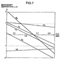
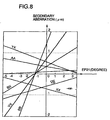
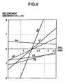
- Figs. 6 to 11 show the variation of the secondary aberration brought about by an incident angle EP11 of the first magnetic field, a ratio (DL2/AM1) of a free space distance between the first and the second magnetic fields to a trace radius of the first magnetic field, a ratio (AM1/RM1) of a trace radius of the first magnetic field to a convex radius of an incident end, and a ratio (AM1/RM2) of a trace radius of the first magnetic field to a concave radius of an outgoing end.
- the secondary aberration shown in Figs. 6 to 11 are indicated by using the secondary aberration coefficients of the expressions (1) and (2). IN actual, they are represented in ⁇ m on the assumption of the beam spread appearing in using this filter for practical purpose.
- the aberration with a bar on it is a value on the dispersion point.
- the aberration with no bar on it is a value on the image point.
- the optimal form is determined on the result of simulating those values.
- the allowance for the secondary aberration is not unconditionally determined. It depends on the purpose of the device itself. As is apparent from Figs. 6 to 11, the secondary aberration is gradually varied with respect to the abovementoned parameters. It is practically negligible if it stays in the range of ⁇ 2 ⁇ m.
- the secondary aberration may be reduced to a value within ⁇ 2 ⁇ m. If it is defined in the range of -12° to 0°, it may be further reduced to a value within ⁇ 1 ⁇ m. As is understood from Fig. 7, it is possible to suppress the secondary aberration within ⁇ 2 ⁇ m if a ratio (DL2/AM1) of a middle free space distance to a trace radius of the first magnetic field is set in the range of 0.4 to 0.8. Further, as is understood from Fig.
- Fig. 12 shows the construction of the electron microscope attached with the energy filter.
- this electron energy filter has in-column magnetic poles 21 and 22 located between a middle lens system 53 and a projecting lens system 55.
- An electron beam 4 is fired by an electron gun 59 and then converged through the converging lens system 50.
- the converted beam 4 transmits through a specimen 51 and then is converged to a crossover point 5 through the middle lens system 53.
- the converted beam goes around the inside of the energy filter and then converted again at an energy dispersion point 8.
- a variable slit 54 is located at the energy dispersion point 8 for selectively adjusting the energy width of the line spectrum to a specific one.
- the incident image surface 6 formed through the middle lens system 53 is formed again on the outlet image surface 7 through the effect of the energy filter.
- This image is not made vague by the so-called achromatic effect, that is, the effect that the dispersions are offset by the energy filter if the electrons have the corresponding energy width.
- the electron beam selected as the specific energy through the variable slit 54 passes a projecting lens 55, through which an outlet image 7 is expansively formed on a fluorescent plate 56.
- a numeral 57 denotes a detector.
- the electron energy filter provides two magnetic poles 21 and 22 that are independent of each other.
- Each magnetic pole has a coil wound therearound.
- the magnetic pole yields a magnetic field for an acceleration voltage of the electrons so that the electron beam travels along a specific trace.
- Fig. 13 shows an example of a photo representing an energy-filtered image formed by the electron microscope attached with the energy filter according to this embodiment.
- the used specimen is a carbon grating film about 0.5- ⁇ m square.
- the selected energy is electrons with zero loss.
- the electron beam travels around the inside of the energy filter, the image is represented as a square.
- the electron beam When detecting the electron beam transmitting through the slit under the constant magnetic field and the increased voltage for accelerating the electrons, the electron beam is represented as an energy spectrum of the transmitted electrons, which is illustrated in Fig. 14.
- the conventional electron microscope is served to form all the electrons having any magnitude of energy contained in this energy spectrum as an image and expand it.
- the electron energy filter enables to select only the electrons having a specific magnitude of energy.
- Figs. 15A to 15C show electron microscopic photos of a non-dyeing specimen with a thickness of about 70 ⁇ m where a cardiac muscle of a mouse is double-fixed by glutaraldehyde and osmium tetroxide.
- Fig. 15A shows an ordinary image of the electron microscope.
- Fig. 15A shows an image formed of only the electrons with zero loss selected through the electron energy filter.
- Fig. 15C is a loss image formed of only the electrons close to -250 eV.
- the electron microscope attached with the energy filter of this embodiment may offer an image with improved contrast rather than the conventional electron microscope. Further, in the former, by selecting the core-loss electrons, it is possible to form a vivid mapping image of specific elements and improve a function of an analytic electron microscope.
- the resulting electron energy filter may be compactly designed with a small number of magnetic poles and is low in aberration and excellent in a converging characteristic.
- the deflecting angle WM1 and the central trace radius AM1 in the first magnetic field, the deflecting angle WM2 and the central trace radius AM2 in the second magnetic field, the distance DL2 from the outgoing point of the first magnetic field to the incident point of the second magnetic field are selected in the following numerical ranges.
- WM1 substantially 90° 1.5 AM2 ⁇ AM1 ⁇ 2.5 AM2
- WM2 substantially 180° Am1 ⁇ DL2 ⁇ 2 AM1
- the first incident angle EP11 and the outgoing angle EP12 of the electron beam in the first magnetic field and the incident and outgoing angle EP21 of the electron beam in the second magnetic field are selected in the following numerical ranges. 20° ⁇ EP11 ⁇ 30° 20° ⁇ EP12 ⁇ 30° -3° ⁇ EP21 ⁇ 1°
- the magnetic pole end of the first incident point and the outgoing point of the electron beam in the first magnetic field is worked as a convex or a concave.
- These curvature radii RM1 and RM2 are selected in the following numerical ranges. Incident Plane -1 ⁇ AM1/RM1 ⁇ 1 Outgoing Plane -1 ⁇ AM1/RM2 ⁇ 1 where a sign of + represents the convex curvature and a sign of - represents the concave curvature.
- the energy filter is designed so that the electron beam that outgoes at the crossover point is, again, focused at one point on the energy dispersion surface. This design is based on the following disadvantages appearing if the electron beam is linearly focused without focusing it at one point,
- the first-order aberration coefficients at the image point DLI4 and the energy dispersion point DLD4 are indicated as follows, where DLI4 is a distance from the final magnetic pole end to the image point and DLD4 is a distance from the final magnetic pole end to the energy dispersion point.
- the secondary aberration coefficients of the electron energy filter of this embodiment calculated by the TRIO are illustrated in Table 3. Those secondary aberration coefficients are small enough to inhibit the distorted or vague energy spectrum and image and are maintained in the allowable range. Further, the electron energy filter includes four deflecting magnetic fields, that is, the number of the magnetic poles is as small as four. The electron energy filter is excellent in workability and constructed compactly.
- the deflecting angle WM1 and the central trace radius AM1 in the first magnetic field, the deflecting angle WM2 and the central trace radius AM2 in the second magnetic field, and a distance from the outgoing point of the first magnetic field to the incident point of the second magnetic field are selected in the following numerical ranges. 75° ⁇ WM1 ⁇ 85°, preferably, substantially 80° 1.5 AM2 ⁇ AM1 ⁇ 2.5 AM2 190° ⁇ WM2 ⁇ 210°, preferably, substantially 200° 0.8 AM1 ⁇ DL2 ⁇ 2.5 AM1
- the first incident angle EP11 and the outgoing angle EP12 of the electron beam in the first magnetic field and the incident and outgoing angle EP21 of the electron beam in the second magnetic field are selected in the following numerical range. 15° ⁇ EP11 ⁇ 15° 30° ⁇ EP12 ⁇ 45° -7° ⁇ EP21 ⁇ 3°
- the magnetic pole end of the first incident point and the outgoing point of the electron beam in the first magnetic field is worked as a convex or a concave for reducing the secondary aberration to a minimum.
- These curvature radii RM11 and RM12 are selected in the following numerical range, where a sign of + represents the convex curvature and a sign of - represents the concave curvature.
- the curvature radius RM21 of the magnetic pole end between the incident point and the outgoing point of the electron beam in the second magnetic field is selected in the following numerical range by the trace radius AM2. 0.5 ⁇ AM2/RM21 ⁇ 1.5
- This electron energy filter is designed so that the electron beam that outgoes at the crossover point is, again, focused at one point on the energy dispersion surface. If the electron beam is focused not at one point but linearly, the following disadvantages take place.
- the first-order aberration coefficients at the image point DLI4 and the energy dispersion point DLD4 are indicated as follows, where DLI4 is a distance from the final magnetic pole end to the image point and DLD4 is a distance from the final magnetic pole end to the energy dispersion point.
- DL14 9.83 mm
- the secondary aberration coefficients of the electron energy filter according to this example which are calculated by the TRIO, are listed in Table 4. Those secondary aberration coefficients are small enough to inhibit the distorted or vague energy spectrum or image and maintained in the allowable range.
- This electron energy filter is constructed to have two deflecting magnetic fields for realizing the foregoing optical system, that is, the number of the magnetic poles is as small as four.
- the electron energy filter is excellent in workability and is constructed compactly.
- the deflecting angle WM1 and the central trace radius AM1 in the first magnetic field, the deflecting angle WM2 and the central trace radius AM2 in the second magnetic field, and the distance DL2 from the outgoing point of the first magnetic field to the incident point of the second magnetic field are selected in the following numerical range.
- the first incident angle EP11 and the outgoing angle Epl2 of the electron beam in the first magnetic field and the incident and outgoing angle EP21 of the electron beam in the second magnetic field are selected in the following numerical ranges. 38° ⁇ EP11 ⁇ 45° 8° ⁇ EP12 ⁇ 16° 25° ⁇ EP21 ⁇ 35°
- the magnetic pole end between the first incident point and the outgoing point of the electron beam in the first magnetic field is worked as a concave or a convex for reducing the secondary aberration to a minimum.
- These curvature radii RM11 and RM12 are selected in the following numerical ranges, where a sign of + represents a convex curvature and a sign of - represents a concave curvature.
- the electron energy filter is designed so that the electron beam that outgoes at the crossover point is, again, focused at one point on the energy dispersion surface. If the electron beam is focused not at one point but linearly, the following disadvantages take place.
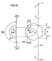
- Fig. 16 shows a schematic construction of the filter constructed to use these parameters, in which the same members of Fig. 16 as those of Fig. 1A have the same reference numbers and thus are not descriptive herein.
- the first-order aberration coefficients at the image point DLI4 and the energy dispersion point DLD4 are indicated as follows, where DLI4 is a distance from the final magnetic pole end to the image point and DLD4 is a distance from the final magnetic pole end to the energy dispersion point.
- DL14 42.1 mm
- X -1.0
- Y -1.0
- B 0.0
- the secondary aberration coefficients of the electron energy filter according to this embodiment which are calculated by the TRIO, are listed in Table 5. Those secondary aberration coefficients are small enough to inhibit the distorted or vague energy spectrum and image and thus maintained in an allowable range. Further, the electron energy filter is constructed to have two deflecting magnetic fields for realizing the foregoing optical system, that is, the number of the magnetic poles is as small as four. The electron energy filter is excellent in workability and is constructed compactly.
Landscapes
- Chemical & Material Sciences (AREA)
- Analytical Chemistry (AREA)
- Electron Tubes For Measurement (AREA)
Claims (17)
- Filtre à énergie électronique pour dévier des électrons et filtrer uniquement les électrons ayant une énergie spécifique, comportant :dans lequel des électrons incidents sont déviés à un premier angle de déviation WM1 sensiblement de 90° avec un premier rayon de trace AM1 par l'intermédiaire de l'effet dudit premier champ magnétique de déviation, ayant traversé un premier trajet dudit espace libre, et ensuite sont incidents sur ledit second champ magnétique de déviation, après quoi ils sont déviés à un second angle de déviation WM2 sensiblement de 180° avec un second rayon de trace AM2, ayant traversé un second trajet dudit espace libre, ledit second trajet étant sensiblement parallèle audit premier trajet, et sont incidents sur ledit premier champ magnétique de déviation, ensuite sont réfléchis audit premier angle de déviation WM1 avec ledit premier rayon de trace AM1 et continuant sensiblement dans la même direction que les électrons incidents sur ledit premier champ magnétique de déviation, le minimum de la distance DL2 dudit espace libre parcouru par lesdits électrons entre lesdits premier et second champs magnétiques de déviation étant d'environ la moitié du premier rayon de trace AM1.des moyens (21, 25) pour générer un premier champ magnétique de déviation,des moyens (22, 26) pour générer un second champ magnétique de déviation ayant la même direction de déviation que ledit premier champ magnétique de déviation, etun espace libre sur lequel lesdits champs magnétiques desdits moyens (21, 25 ; 22, 26) n'ont aucun effet important,
- Filtre selon la revendication 1, dans lequel ledit premier trajet est sensiblement égal en distance audit second trajet.
- Filtre selon la revendication 1, dans lequel ledit premier trajet est sensiblement égal en distance audit second trajet, et ladite distance DL2 et ledit premier rayon de trace AM1 satisfont à la relation suivante :
- Filtre selon la revendication 1, dans lequel
lesdits moyens (21, 25) destinés à générer le premier champ magnétique de déviation comportent une première paire de pôles magnétiques (21) et lesdits moyens (22, 26) destinés à générer le second champ magnétique de déviation comportent une seconde paire de pôles magnétiques (22) et lesdits premier et second champs magnétiques de déviation sont dirigés dans la même direction, et
ledit premier rayon de trace AM1, ledit second rayon de trace AM2 et ladite distance d'espace libre DL2 satisfont aux relations suivantes : - Filtre selon la revendication 4, dans lequel un premier angle incident EP11 et un premier angle de sortie EP12 d'un faisceau desdits électrons par rapport audit premier champ magnétique de déviation et un angle incident et de sortie EP21 dudit faisceau d'électrons par rapport audit second champ magnétique de déviation satisfont aux relations suivantes :
- Filtre selon la revendication 4, dans lequel un premier angle incident EP11 d'un faisceau desdits électrons est d'environ 42°, un premier angle de sortie EP12 dudit faisceau est d'environ 11,8°, les deux se rapportant audit premier champ magnétique de déviation, et un angle incident et de sortie EP21 dudit faisceau par rapport audit second champ magnétique de déviation est d'environ 30°.
- Filtre selon la revendication 5, dans lequel une extrémité de pôle magnétique en un premier point incident dudit faisceau électronique par rapport audit premier champ magnétique de déviation a un rayon de courbure RM1, une extrémité de pôle magnétique en un premier point de sortie a un rayon de courbure RM2, et lesdits rayons de courbure RM1 et RM2 satisfont aux relations suivantes :
- Filtre selon la revendication 6, dans lequel une extrémité de pôle magnétique au point incident dudit faisceau d'électrons par rapport audit premier champ magnétique de déviation a un rayon de courbure RM1, une extrémité de pôle magnétique au point de sortie a un rayon de courbure RM2, et lesdits rayons de courbure RM1 et RM2 satisfont aux relations suivantes :
- Filtre selon la revendication 4, dans lequel la distance DL2 dudit espace libre est égale audit premier rayon de trace AM1.
- Filtre selon la revendication 1, dans lequel lesdits moyens de génération des premier et second champs magnétiques de déviation (21, 25 ; 22, 26) comportent :dans lequel ledit premier rayon de trace AM1, ledit second rayon de trace AM2, et la distance DL2 dudit espace libre satisfont aux relations suivantes :une première paire de pôles magnétiques (21) pour générer ledit premier champ magnétique de déviation et une seconde paire de pôles magnétiques (22) pour générer ledit second champ magnétique de déviation dans la même direction que ledit premier champ magnétique de déviation,
- Filtre selon la revendication 7, dans lequel un premier angle incident EP11 et un premier angle de sortie EP12 desdits électrons par rapport audit premier champ magnétique de déviation et un angle incident et de sortie EP21 desdits électrons par rapport audit second champ magnétique de déviation satisfont aux relations suivantes :
- Filtre selon la revendication 11, dans lequel une extrémité de pôle magnétique en un premier point incident desdits électrons par rapport audit premier champ magnétique de déviation a un rayon de courbure RM1, une extrémité de pôle magnétique en un premier point de sortie desdits électrons par rapport audit premier champ magnétique de déviation a un rayon de courbure RM2, et lesdits rayons de courbure RM1 et RM2 satisfont aux relations suivantes :
- Filtre selon la revendication 10, dans lequel la distance DL2 dudit espace libre est plus longue que ledit premier rayon de trace AM1.
- Filtre selon la revendication 10, dans lequel un premier angle incident EP11 et un premier angle de sortie EP12 desdits électrons par rapport audit premier champ magnétique de déviation et un angle incident et de sortie EP21 desdits électrons par rapport audit second champ magnétique de déviation satisfont aux relations suivantes :
- Filtre selon la revendication 14, dans lequel une extrémité de pôle magnétique en un premier point incident desdits électrons par rapport audit premier champ magnétique de déviation a un rayon de courbure RM11, une extrémité de pôle magnétique en un premier point de sortie a un rayon de courbure RM12, une extrémité de pôle magnétique en un point incident et en un point de sortie desdits électrons par rapport audit second champ magnétique de déviation a un rayon de courbure RM21, et lesdits rayons de courbure RM11, RM12 et RM21 satisfont aux relations suivantes :
- Microscope électronique de transmission incluant le filtre à énergie électronique selon l'une quelconque des revendications 1 à 15.
- Procédé pour filtrer l'énergie d'un faisceau d'électrons, comportant les étapes consistant à :dans lequel le minimum de la distance DL2 dudit espace libre parcouru par lesdits électrons entre lesdits premier et second champs magnétiques de déviation est environ égal à la moitié du premier rayon de trace AM1.dévier des électrons incidents à un premier angle de déviation WM1 sensiblement de 90° avec un premier rayon de trace AM1 par un premier champ magnétique de déviation et les laisser passer à travers un premier trajet d'un espace libre sensiblement non-affecté par un champ magnétique,dévier lesdits électrons ayant traversé ledit premier trajet à un second angle de déviation WM2 sensiblement de 180° et ayant le même sens que ledit premier angle de déviation WM1 et avec un second rayon de trace AM2 par un second champ magnétique de déviation et laisser lesdits électrons déviés passer à travers un second trajet dudit espace libre, ledit second trajet étant sensiblement parallèle audit premier trajet, etdévier lesdits électrons ayant traversé ledit second trajet à un premier angle de déviation WM1 avec ledit rayon de trace AM1 par l'effet dudit premier champ magnétique de déviation et laisser sortir lesdits électrons déviés sensiblement dans la même direction que les électrons incidents,
Applications Claiming Priority (4)
| Application Number | Priority Date | Filing Date | Title |
|---|---|---|---|
| JP18514094 | 1994-07-15 | ||
| JP185140/94 | 1994-07-15 | ||
| JP18514094 | 1994-07-15 | ||
| PCT/JP1995/001401 WO1996002935A1 (fr) | 1994-07-15 | 1995-07-14 | Filtre a energie electronique |
Publications (3)
| Publication Number | Publication Date |
|---|---|
| EP0772225A1 EP0772225A1 (fr) | 1997-05-07 |
| EP0772225A4 EP0772225A4 (fr) | 1997-10-29 |
| EP0772225B1 true EP0772225B1 (fr) | 2003-03-19 |
Family
ID=16165580
Family Applications (1)
| Application Number | Title | Priority Date | Filing Date |
|---|---|---|---|
| EP95925121A Expired - Lifetime EP0772225B1 (fr) | 1994-07-15 | 1995-07-14 | Filtre a energie electronique |
Country Status (4)
| Country | Link |
|---|---|
| US (1) | US6066852A (fr) |
| EP (1) | EP0772225B1 (fr) |
| DE (1) | DE69529987T2 (fr) |
| WO (1) | WO1996002935A1 (fr) |
Cited By (1)
| Publication number | Priority date | Publication date | Assignee | Title |
|---|---|---|---|---|
| CZ302974B6 (cs) * | 2000-02-08 | 2012-02-01 | Carl Zeiss Nts Gmbh | Filtr energie elektronu s magnetickými vychylovacími oblastmi a elektronový mikroskop |
Families Citing this family (11)
| Publication number | Priority date | Publication date | Assignee | Title |
|---|---|---|---|---|
| DE19746785A1 (de) * | 1997-10-23 | 1999-04-29 | Leo Elektronenmikroskopie Gmbh | Teilchenstrahlgerät mit Energiefilter |
| DE19855629A1 (de) * | 1998-12-02 | 2000-06-08 | Leo Elektronenmikroskopie Gmbh | Teilchenoptische Anordnung und Verfahren zur teilchenoptischen Erzeugung von Mikrostrukturen |
| JP3441955B2 (ja) * | 1998-02-23 | 2003-09-02 | 株式会社日立製作所 | 投射方式の荷電粒子顕微鏡および基板検査システム |
| JP2002025485A (ja) * | 2000-07-06 | 2002-01-25 | Jeol Ltd | エネルギーフィルタ |
| US6717141B1 (en) * | 2001-11-27 | 2004-04-06 | Schlumberger Technologies, Inc. | Reduction of aberrations produced by Wien filter in a scanning electron microscope and the like |
| JP2003297271A (ja) * | 2002-04-03 | 2003-10-17 | Hitachi High-Technologies Corp | モノクロメータ付走査形電子顕微鏡 |
| JP3789104B2 (ja) * | 2002-05-13 | 2006-06-21 | 株式会社日立ハイテクノロジーズ | 元素分布観察方法及び装置 |
| US20060063802A1 (en) | 2004-03-29 | 2006-03-23 | Matthieu Guitton | Methods for the treatment of tinnitus induced by cochlear excitotoxicity |
| PL368785A1 (pl) * | 2004-06-28 | 2006-01-09 | Krzysztof Grzelakowski | Obrazujący filtr energii dla elektronów i innych elektrycznie naładowanych cząstek oraz sposób filtrowania energii elektronów i innych elektrycznie naładowanych cząstek w urządzeniach elektrooptycznych za pomocą obrazującego filtru energii |
| EA017264B1 (ru) * | 2005-09-28 | 2012-11-30 | Аурис Медикаль Аг | Применение композиции арилциклоалкиламида для получения лекарственного препарата для лечения нарушения внутреннего уха |
| CN109613597B (zh) * | 2018-11-30 | 2021-04-06 | 上海联影医疗科技股份有限公司 | 一种确定电子束能谱的方法及系统 |
Family Cites Families (11)
| Publication number | Priority date | Publication date | Assignee | Title |
|---|---|---|---|---|
| FR2453492A1 (fr) * | 1979-04-03 | 1980-10-31 | Cgr Mev | Dispositif de deviation magnetique achromatique d'un faisceau de particules chargees et appareil d'irradiation utilisant un tel dispositif |
| US4312218A (en) * | 1979-09-04 | 1982-01-26 | Li-Cor, Inc. | Porometer and method for stomatal measurements |
| US4425506A (en) * | 1981-11-19 | 1984-01-10 | Varian Associates, Inc. | Stepped gap achromatic bending magnet |
| DE3423149A1 (de) * | 1984-06-22 | 1986-01-02 | Fa. Carl Zeiss, 7920 Heidenheim | Verfahren und anordnung zur elektronenenergiegefilterten abbildung eines objektes oder eines objektbeugungsdiagrammes mit einem transmissions-elektronenmikroskop |
| JPS61277141A (ja) * | 1985-05-31 | 1986-12-08 | Jeol Ltd | 磁界型エネルギ−フイルタ− |
| DE3532698A1 (de) * | 1985-09-13 | 1987-03-26 | Zeiss Carl Fa | Elektronenenergiefilter vom alpha-typ |
| DE3532699A1 (de) * | 1985-09-13 | 1987-03-26 | Zeiss Carl Fa | Elektronenenergiefilter vom omega-typ |
| US5097126A (en) * | 1990-09-25 | 1992-03-17 | Gatan, Inc. | High resolution electron energy loss spectrometer |
| DE4041495A1 (de) * | 1990-12-22 | 1992-06-25 | Zeiss Carl Fa | Elektronenenergiefilter, vorzugsweise vom alpha- oder omega-typ |
| JP3397347B2 (ja) * | 1992-11-26 | 2003-04-14 | 日本電子株式会社 | オメガフィルタ |
| JP3139920B2 (ja) * | 1994-07-25 | 2001-03-05 | 株式会社日立製作所 | エネルギフィルタおよびこれを備えた透過電子顕微鏡 |
-
1995
- 1995-07-14 US US08/765,914 patent/US6066852A/en not_active Expired - Fee Related
- 1995-07-14 EP EP95925121A patent/EP0772225B1/fr not_active Expired - Lifetime
- 1995-07-14 DE DE69529987T patent/DE69529987T2/de not_active Expired - Fee Related
- 1995-07-14 WO PCT/JP1995/001401 patent/WO1996002935A1/fr active IP Right Grant
Cited By (1)
| Publication number | Priority date | Publication date | Assignee | Title |
|---|---|---|---|---|
| CZ302974B6 (cs) * | 2000-02-08 | 2012-02-01 | Carl Zeiss Nts Gmbh | Filtr energie elektronu s magnetickými vychylovacími oblastmi a elektronový mikroskop |
Also Published As
| Publication number | Publication date |
|---|---|
| DE69529987D1 (de) | 2003-04-24 |
| DE69529987T2 (de) | 2004-01-15 |
| US6066852A (en) | 2000-05-23 |
| WO1996002935A1 (fr) | 1996-02-01 |
| EP0772225A1 (fr) | 1997-05-07 |
| EP0772225A4 (fr) | 1997-10-29 |
Similar Documents
| Publication | Publication Date | Title |
|---|---|---|
| EP1381073B1 (fr) | Appareil optique pour particules chargées ayant une correction d'aberration | |
| EP0772225B1 (fr) | Filtre a energie electronique | |
| US6329659B1 (en) | Correction device for correcting the lens defects in particle-optical apparatus | |
| DE69733873T2 (de) | Vorrichtung zur korrektur von linsenfehlern in teilchen-optischer geräte | |
| US5449914A (en) | Imaging electron energy filter | |
| US4684808A (en) | Scanning system for a particle beam scanning apparatus | |
| US4851670A (en) | Energy-selected electron imaging filter | |
| JPH05205687A (ja) | 鏡補正器を有する、荷電素粒子ビーム用結像系 | |
| JP4416208B2 (ja) | 磁気形結像エネルギフィルタを有する電子顕微鏡 | |
| JPH05314938A (ja) | 電子ビーム装置 | |
| JP2008078058A (ja) | 電子線装置及びこれを用いたパターン評価方法 | |
| JPH01319236A (ja) | 電界放射電子銃 | |
| US6559445B2 (en) | Electron energy filter with magnetic deflecting regions | |
| JP3400284B2 (ja) | オメガ型エネルギーフィルタ及び該フィルタを組み込んだ電子顕微鏡 | |
| JP3896043B2 (ja) | 電子顕微鏡の球面収差補正装置 | |
| JP2018129171A (ja) | エネルギーフィルタおよび荷電粒子線装置 | |
| GB2081971A (en) | Electron optics of electron microscope | |
| EP1058287B1 (fr) | Filtre d'énergie magnétique | |
| Schmid et al. | Correction and alignment strategies for the beam separator of the photoemission electron microscope 3 (PEEM3) | |
| US6586737B2 (en) | Transmission electron microscope equipped with energy filter | |
| EP3731255B1 (fr) | Filtre d'énergie et appareil à faisceau de particules chargées | |
| US4251790A (en) | Magnetic focusing and deflection system for electron beam tubes | |
| JP2004517456A (ja) | 静電矯正器 | |
| JPS61277141A (ja) | 磁界型エネルギ−フイルタ− | |
| JP2001351555A (ja) | エネルギーフィルタを備えた電子顕微鏡 |
Legal Events
| Date | Code | Title | Description |
|---|---|---|---|
| PUAI | Public reference made under article 153(3) epc to a published international application that has entered the european phase |
Free format text: ORIGINAL CODE: 0009012 |
|
| 17P | Request for examination filed |
Effective date: 19970127 |
|
| AK | Designated contracting states |
Kind code of ref document: A1 Designated state(s): DE NL |
|
| A4 | Supplementary search report drawn up and despatched |
Effective date: 19970912 |
|
| AK | Designated contracting states |
Kind code of ref document: A4 Designated state(s): DE NL |
|
| 17Q | First examination report despatched |
Effective date: 19980402 |
|
| 18D | Application deemed to be withdrawn |
Effective date: 19981013 |
|
| D18D | Application deemed to be withdrawn (deleted) | ||
| GRAG | Despatch of communication of intention to grant |
Free format text: ORIGINAL CODE: EPIDOS AGRA |
|
| GRAG | Despatch of communication of intention to grant |
Free format text: ORIGINAL CODE: EPIDOS AGRA |
|
| GRAG | Despatch of communication of intention to grant |
Free format text: ORIGINAL CODE: EPIDOS AGRA |
|
| GRAH | Despatch of communication of intention to grant a patent |
Free format text: ORIGINAL CODE: EPIDOS IGRA |
|
| GRAH | Despatch of communication of intention to grant a patent |
Free format text: ORIGINAL CODE: EPIDOS IGRA |
|
| GRAA | (expected) grant |
Free format text: ORIGINAL CODE: 0009210 |
|
| AK | Designated contracting states |
Designated state(s): DE NL |
|
| REF | Corresponds to: |
Ref document number: 69529987 Country of ref document: DE Date of ref document: 20030424 Kind code of ref document: P |
|
| PLBE | No opposition filed within time limit |
Free format text: ORIGINAL CODE: 0009261 |
|
| STAA | Information on the status of an ep patent application or granted ep patent |
Free format text: STATUS: NO OPPOSITION FILED WITHIN TIME LIMIT |
|
| 26N | No opposition filed |
Effective date: 20031222 |
|
| PGFP | Annual fee paid to national office [announced via postgrant information from national office to epo] |
Ref country code: NL Payment date: 20050627 Year of fee payment: 11 |
|
| PGFP | Annual fee paid to national office [announced via postgrant information from national office to epo] |
Ref country code: DE Payment date: 20051012 Year of fee payment: 11 |
|
| PG25 | Lapsed in a contracting state [announced via postgrant information from national office to epo] |
Ref country code: NL Free format text: LAPSE BECAUSE OF NON-PAYMENT OF DUE FEES Effective date: 20070201 Ref country code: DE Free format text: LAPSE BECAUSE OF NON-PAYMENT OF DUE FEES Effective date: 20070201 |
|
| NLV4 | Nl: lapsed or anulled due to non-payment of the annual fee |
Effective date: 20070201 |