EP0770879A2 - Vorrichtung zum Messen der Entwicklerladungsmenge - Google Patents
Vorrichtung zum Messen der Entwicklerladungsmenge Download PDFInfo
- Publication number
- EP0770879A2 EP0770879A2 EP96307093A EP96307093A EP0770879A2 EP 0770879 A2 EP0770879 A2 EP 0770879A2 EP 96307093 A EP96307093 A EP 96307093A EP 96307093 A EP96307093 A EP 96307093A EP 0770879 A2 EP0770879 A2 EP 0770879A2
- Authority
- EP
- European Patent Office
- Prior art keywords
- developer
- charge
- lower electrode
- amount
- upper electrode
- Prior art date
- Legal status (The legal status is an assumption and is not a legal conclusion. Google has not performed a legal analysis and makes no representation as to the accuracy of the status listed.)
- Granted
Links
- 230000005684 electric field Effects 0.000 claims abstract description 84
- 238000001514 detection method Methods 0.000 claims abstract description 23
- 239000002245 particle Substances 0.000 claims description 60
- 238000004140 cleaning Methods 0.000 claims description 32
- 238000005259 measurement Methods 0.000 claims description 23
- 230000010355 oscillation Effects 0.000 claims description 13
- 230000003287 optical effect Effects 0.000 claims description 5
- 230000005484 gravity Effects 0.000 claims description 4
- 238000006243 chemical reaction Methods 0.000 claims 4
- 238000007599 discharging Methods 0.000 claims 1
- 239000000463 material Substances 0.000 claims 1
- 238000000034 method Methods 0.000 description 13
- 239000000779 smoke Substances 0.000 description 6
- 238000010586 diagram Methods 0.000 description 5
- 230000000694 effects Effects 0.000 description 4
- 238000007639 printing Methods 0.000 description 3
- 230000001133 acceleration Effects 0.000 description 2
- 230000009286 beneficial effect Effects 0.000 description 2
- 238000007664 blowing Methods 0.000 description 2
- 239000000126 substance Substances 0.000 description 2
- XOLBLPGZBRYERU-UHFFFAOYSA-N tin dioxide Chemical compound O=[Sn]=O XOLBLPGZBRYERU-UHFFFAOYSA-N 0.000 description 2
- IJGRMHOSHXDMSA-UHFFFAOYSA-N Atomic nitrogen Chemical compound N#N IJGRMHOSHXDMSA-UHFFFAOYSA-N 0.000 description 1
- 230000006978 adaptation Effects 0.000 description 1
- 230000000903 blocking effect Effects 0.000 description 1
- 238000010276 construction Methods 0.000 description 1
- 230000004069 differentiation Effects 0.000 description 1
- 229910001873 dinitrogen Inorganic materials 0.000 description 1
- 238000001704 evaporation Methods 0.000 description 1
- 238000007667 floating Methods 0.000 description 1
- 239000011521 glass Substances 0.000 description 1
- 230000010354 integration Effects 0.000 description 1
Images


Classifications
-
- G—PHYSICS
- G01—MEASURING; TESTING
- G01R—MEASURING ELECTRIC VARIABLES; MEASURING MAGNETIC VARIABLES
- G01R29/00—Arrangements for measuring or indicating electric quantities not covered by groups G01R19/00 - G01R27/00
- G01R29/24—Arrangements for measuring quantities of charge
-
- G—PHYSICS
- G03—PHOTOGRAPHY; CINEMATOGRAPHY; ANALOGOUS TECHNIQUES USING WAVES OTHER THAN OPTICAL WAVES; ELECTROGRAPHY; HOLOGRAPHY
- G03G—ELECTROGRAPHY; ELECTROPHOTOGRAPHY; MAGNETOGRAPHY
- G03G15/00—Apparatus for electrographic processes using a charge pattern
- G03G15/06—Apparatus for electrographic processes using a charge pattern for developing
- G03G15/08—Apparatus for electrographic processes using a charge pattern for developing using a solid developer, e.g. powder developer
- G03G15/0822—Arrangements for preparing, mixing, supplying or dispensing developer
- G03G15/0848—Arrangements for testing or measuring developer properties or quality, e.g. charge, size, flowability
Definitions
- the present invention relates to a measuring device for amount of charge of developer used as visualizing particles in an image forming apparatus of an electrophotographic printing system such as a copying machine.
- toner particles are used as a developer, and the toner particles are charged when using them in forming images.
- the amount of charge of the toner particles is the important factor to determine an image quality, and various methods have been developed for measuring an amount of charge.
- a blow-off method As a measuring method for an amount of charge of toner, a blow-off method is known.
- an amount of charge of toner particles in a two-component developer composed of toner particles and carrier particles is measured specifically in the following manner. First, the two-component developer is placed on a holding member with meshes bigger than the diameter of a toner particle and smaller than a diameter of a carrier particle, and only the toner particles are blown off by dry air blow (for example, nitrogen gas). Then, an amount of charge of the residual carrier particles remaining on the support member is measured to determine an amount of charge by weight of toner.
- dry air blow for example, nitrogen gas
- an amount of charge of the residual carrier particles remaining on the support member is measured to determine an amount of charge by weight of toner.
- the described blow-off method has been widely used as a measuring method of an amount of charge per unit weight.
- the blow-off method has the following drawbacks: That is, a measured value fluctuates with flow of dry air blow and a measuring time, and this makes it difficult to measure an amount of charge of toner successively. Besides, this method cannot be applied to the one-component developer of toner particles without including the carrier particles, and even for the two-component developer, distribution of the amount of charge cannot be measured.
- the measuring method of the Gazette (1) charged particles are dropped by the dead weight in an electric field, and the dropping velocity and the trace thereof are detected by an image pickup unit. Then, an amount of charge is calculated based on the result of detection.
- the toner particles are conveyed in the DC electric field by an air-flow, and a distance the toner particle moves is detected by a line image sensor to determine the specific charge distribution of the toner particles.
- the electric field is applied to the toner particle flow, and the toner particle group in the electric field is observed by a magnifying optical system to determine the amount of charge of toner based on the information indicative of distance the toner moves and the particle diameter.
- the toner particles are picked up by the image pick-up unit, and the resulting information is processed by the image processing unit to obtain the amount of charge of toner particles, etc.
- the conventional arrangements require valuable devices such as the image pick-up unit, the image processing unit, etc., thereby presenting the problem of high cost.
- An object of the present invention is to provide a measuring device for amount of charge of developer at low cost.
- a measuring device for amount of charge of developer of the present invention includes:
- the developer particles, an amount of charge of which is to be measured are placed on the lower electrode.
- an electric field is generated so that the developer is flied from the lower electrode towards the upper electrode.
- the developer on the lower electrode adheres to the upper electrode.
- a current in accordance with an amount of charge of the adhered developer flows in the upper electrode, and is detected by the current detection means.
- the arithmetic unit computes a total amount of charge of the developer adhered to the upper electrode based on a change in amount of current detected by the current detection unit, i.e., an amount of increase of the current by the charged developer adhering to the upper electrode.
- a measuring device for amount of charge of developer can be achieved at low cost compared with the conventional measuring device in which an image of the developer is picked up by the image pick-up unit, and an amount of charge of the developer is measured by the image processing unit.
- Fig. 1 is an explanatory view schematically showing an entire structure of a measuring device for amount of charge of developer in accordance with one embodiment of the present invention with a perspective view of a measuring chamber and a block diagram of respective means connected thereto.
- Fig. 2 is a circuit diagram of a flying electric field power source unit and a current detection unit connected to the measuring chamber shown in Fig. 1.
- Fig. 3 is an explanatory view showing an operation where the toner is moved from a lower electrode to an upper electrode between the lower electrode and the upper electrode shown in Fig. 1.
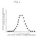
- Fig. 4 is a graph showing a correlation between an output value of an AD converter shown in Fig. 2 and an application voltage to the upper electrode.
- Fig. 5 is a waveform diagram of a current that flows as the toner reaches the upper electrode shown in Fig. 2.
- Fig. 6 is a graph showing a change in total amount of charge obtained by summing a current value shown in Fig. 5 with an applied predetermined flying electric field voltage.
- Fig. 7 is a circuit diagram showing a structure of a measuring device for amount of charge of developer in accordance with another embodiment.
- Fig. 8 is an explanatory view schematically showing a structure of a measuring chamber of a measuring device for amount of charge of developer in accordance with a still another embodiment.
- Fig. 9 is an explanatory view schematically showing an entire structure of a measuring chamber of a measuring device for amount of charge of developer in accordance with a still another embodiment with a perspective view of a measuring chamber and a block diagram of respective means connected thereto.
- Fig. 10 is a longitudinal cross-sectional view of the structure shown in Fig. 9.
- a measuring device for amount of charge of developer in accordance with the present embodiment is provided with a measuring chamber 1.
- the measuring chamber 1 includes an upper wall portion 2, a lower wall portion 3 and two side wall portions 4 and 5.
- the lower wall portion 3 is horizontally formed, and the upper wall portion 2 and the lower wall portion 3 are formed in parallel so as to face each other.
- the side wall portions 4 and 5 are also formed in parallel so as to face each other. In the described arrangement, as no side walls adjacent to the side wall portions 4 and 5 are formed therebetween, and openings 6 and 7 are formed.
- the lower wall portion 3 has a lower electrode 8 exposed to the upper surface thereof.
- the upper wall portion 2 has an upper electrode 9 that is exposed to the lower surface thereof and faces the lower electrode 8.
- the lower electrode 8 is capable of oscillating up and down.
- the lower electrode 8 includes an electrode section 8a and an insulating layer 8b, for example, with a thickness of 30 ⁇ m, formed on the upper surface of the electrode section 8a.
- an oscillator 10 On the back surface of the lower electrode 8, provided is an oscillator 10. A movable portion of the oscillator 10 is connected to the back surface of the lower electrode 8. To the oscillator 10, connected is an oscillator driver 11 for supplying thereto a drive voltage. The oscillator 10 and the oscillator driver 11 constitute oscillation means. Upon receiving the drive voltage, the oscillator 10 oscillates up and down.
- the oscillation frequency of the oscillator 10 is preferably in a range of from 100 to 1,000 Hz, more preferably in a range of from 700 to 900 Hz, and most preferably 800 Hz.
- the measuring device for amount of charge of developer further includes a flying electric field power source unit 12 (flying electric field voltage application means) for applying a flying electric field voltage which generates an electric field between the lower electrode 8 and the upper electrode 9 so as to fly a toner T from the lower electrode 8 to the upper electrode 9.
- the toner T that flied from the lower electrode 8 adheres to the upper electrode 9.
- a current flows in the upper electrode 9 and is detected by a current detection unit 13 (current detection means).
- the current detection unit 13 includes an amplifier 14, a resistor 15, a condenser 16, a reset switch 17 and an analog/digital converter (hereinafter referred to as an AD converter) 18.
- the AD converter 18 is provided for converting an electric analog signal to an electric digital signal.
- An arithmetic unit 19 (arithmetic means) is connected to the current detection unit 13, and a control unit 20 is connected to the arithmetic unit 19.
- the arithmetic unit 19 is provided for computing an amount of charge based on an output from the AD converter 18 in a manner to be described later.
- the control unit 20 is provided for controlling respective operations of the flying electric field power source unit 12, the reset switch 17, the oscillator driver 11, the switch 21 and a toner supply unit 22 (to be described later), etc.
- the output voltage of the flying electric field power source unit 12 is variable.
- the flying electric field power source unit 12 is shown in Fig. 2 such that a voltage of an opposite polarity to the toner, i.e., a positive voltage is applied to the upper electrode 9; however, voltages of both positive and negative are applicable and suitably selected. Namely, for example, when the group of toner particles shows a negative polarity as a whole, it does not mean that all the toner particles show negative polarity, and those having positive polarity may be included. Therefore, in order to permit the measurement of toner particles of opposite polarities, it is required that the flying electric field power source unit 12 can apply voltages of both negative and positive polarities to the upper electrode 9.
- the flying electric field power source unit 12 is connected to the upper electrode 9 through the switch 21.
- One input terminal 14a of the amplifier 14 is connected to an output terminal of a negative electrode of the flying electric field power source unit 12 through the resistor 15. Between the input terminal 14a and an output terminal 14c of the amplifier 14, connected in parallel are the condenser 16 and the reset switch 17. The other input terminal 14b of the amplifier 14 is connected to the lower electrode 8. To the output terminal 14c of the amplifier 14, connected is an input section of the AD converter 18, and to the output section of the AD converter 18, connected is an input section of the arithmetic unit 19.
- the measuring chamber 1 shown in Fig. 1 includes the toner supply unit 22.
- the toner supply unit 22 is arranged so as to supply the group of toner T to be measured onto the lower electrode 8 in the measuring chamber 1. After the measurement, the toner supply unit 22 removes the used toner T for the measurement remaining on the lower electrode 8.
- the toner supply unit 22 is provided with air-suction means or air-blowing means such as an air pump, etc. The toner supply unit 22 enables the toner to be transported with an air-flow A onto the lower electrode 8 through the opening 6 of the measuring chamber 1.
- the air-flow A is required to be strong enough to transport a sufficient amount of toner T . Therefore, the suction means or the air-blowing means of simple structure may be adopted.
- the suction means or the air-blowing means of simple structure may be adopted.
- an air-flow generated with rotations of a rotatable member, such as a developer roller, etc. may be used.
- the properties of the toner particles would not change by the measurement. This permits the toner T to be used again by placing it back in the developer unit after the measurement.
- the inside of the measuring chamber 1 is cleaned. Specifically, the air-flow A is supplied to the inside of the measuring chamber 1 by the toner supply unit 22 to remove foreign substances on the lower electrode 8.
- the lower electrode 8 and the upper electrode 9 are of the same potentials, for example, 0 V (earth potential).
- the group of the toner T to be measured is placed on the lower electrode 8 of the measuring chamber 1 by the toner supply unit 22 so as to generate the air-flow A from the opening 6 towards the opening 7, thereby blocking the air-flow A when the group of the toner T reaches on the lower electrode 8.
- the oscillator driver 11 is actuated, and subsequently, the switch 21 is set ON to actuate the flying electric field power source unit 12 and the current detection unit 13.
- the flying electric field power source unit 12 Upon actuating the flying electric field power source unit 12, a flying electric field voltage is applied to the upper electrode 9.
- a toner flying electric field is generated between the lower electrode 8 and the upper electrode 9, so as to fly the toner T from the lower electrode 8 towards the upper electrode 9.
- the described electric field makes the toner T on the lower electrode 8 to fly towards the upper electrode 9 to be attracted thereto.
- the lower electrode 8 oscillates up and down, i.e., in a vertical direction in a range of from + ⁇ x to - ⁇ x at a predetermined frequency.
- This oscillation of the lower electrode 8 makes the toner particles which form a clod to be scattered on the lower electrode 8.
- a distance L between the lower electrode 8 and the upper electrode 9 varies due to the oscillation of the lower electrode 8, which in turn makes the toner flying electric field to vary.
- the oscillation of the lower electrode 8 also cause the toner T to oscillate; however, as particles of the toner T cannot follow the oscillation of the lower electrode 8 due to a difference between the acceleration by the gravity (mg) and the acceleration by the oscillation of the lower electrode 8, the toner T is kept away from the lower electrode 8. Therefore, the toner T on the lower electrode 8 becomes like smoke.
- each particle of the toner T can fly from the lower electrode 8 to the upper electrode 9 with ease.
- E and q a force exerted onto the toner T by the toner flying electric field is expressed by qE.
- the toner particles T which satisfy the condition of qE > mg reach the upper electrode 9.
- the described oscillation of the lower electrode 8 also suppresses the effect of an image force onto the toner T on the lower electrode 8. This also contributes to urge the toner T to appropriately fly from the lower electrode 8 to the upper electrode 9.
- the image force is exerted so as to attract the toner T onto the lower electrode 8 by the following mechanism. That is, when the charged toner particles come in contact with an electrode plate composed of an electrically conductive member, a charge generates in the electrode plate so as to cancel out the charge of the toner particles.
- the charge in the inside of the electrode plate and the toner particles form a symmetrical distribution with respect to a contact face (electrode plate surface) between the toner particles and the electrode plate so that the charge has an opposite polarity to the toner particles. As a result, an attraction force is exerted onto the toner particles.
- the lower electrode 8 has an insulating layer 8b on the surface thereof, which also contributes to suppress the effect of the image force. Namely, by covering the surface contacting the toner T of the lower electrode 8 with the insulating film 8b, the contact between the toner T and the lower electrode 8 is prevented.
- the image force can be suppressed.
- the toner T can fly from the lower electrode 8 with ease. As a result, the amount of charge of the toner T can be measured accurately.
- the flying electric field power source unit 12 switches the flying electric field voltage to be applied to the upper electrode 9 in a direction of accelerating the toner T to fly from the insulating layer 8b onto the upper electrode 9. Namely, for example, when the group of the toner T is charged only to the negative polarity, a positive low voltage is applied first to the upper electrode 9, and then it is switched to apply a positive high voltage. For example, in the case where the group of the toner T shows a negative polarity as a whole, but includes the toner particles of the positive polarity, a negative voltage is applied first to the upper electrode 9, and then it is switched to apply a positive high voltage.
- the upper limit voltage may be set to 500 V.
- the toner T that reaches the upper electrode 9 has a charge q that satisfies the condition of qE > mg. Therefore, among the group of the toner T on the lower electrode 8, the toner particles reach the upper electrode 9 in order from that having the largest amount of charge. In this case, the toner T that has a small amount of charge which does not satisfy the above inequality does not reach the upper electrode 9. However, by switching the flying electric field voltage as described above, the toner T that has a small amount of charge also reach the upper electrode 9.
- An output voltage of the amplifier 14 is inputted to the AD converter 18, and after being converted to the digital signal, it is inputted to the arithmetic unit 19.
- respective amounts of charge obtained through the AD converter 18 are summed to determine a total amount of charge with an applied predetermined flying electric field voltage.
- the reset switch 17 When the total amount of charge with an applied predetermined flying electric field voltage is calculated in the described manner, the reset switch 17 is set ON, and the charges stored the condenser 16 are released. Thereafter, the reset switch 17 is set OFF again, and the flying electric field voltage is switched subsequently. Then, the total amount of charge is measured with an application of each flying electric field voltage in the described manner.
- a mechanical cleaning unit for example, a cleaning member may be installed in the measuring chamber 1.
- a total amount of charge at each flying electric field voltage is in proportion to the number of toner particles T that reach the upper electrode 9. Therefore, the result of the described measurement enables the distribution of the amount of charge to the group of the toner T to be determined with ease.
- An example of the result of measurement of a distribution of the amount of charge is shown in Fig. 4.
- the results of the measurement shown in Fig. 4 is obtained under the conditions of: a distance L between the lower electrode 8 and the upper electrode 9 is 1 mm; the oscillating frequency of the oscillator 10 is 500 Hz; and the flying electric field voltage is raised each time by 20 V.
- the measuring device for amount of charge of developer of the present embodiment As the toner T becomes like smoke by the oscillation of the lower electrode 8, an amount of charge of each toner T can be obtained. Namely, because of the described beneficial characteristic that the toner T on the lower electrode 8 becomes like smoke, a distance between the electrode 9 and each toner T varies. Therefore, when a predetermined flying electric field voltage is applied to the upper electrode 9, each toner particle reaches the upper electrode 9 at different timing. Therefore, to the upper electrode 9, a pulse-like current shown in Fig. 5 flows in response to the timing that the toner T reaches the upper electrode 9.
- the number of the toner T can be obtained, and further, by dividing the total amount of charge with an application of a predetermined flying electric field voltage to the upper electrode 9 by the number of the toner particles T, an amount of charge of each toner particle T can be obtained.
- the respective amounts of charge to be summed in the arithmetic unit 19 increase, for example, in the state shown in Fig. 6. Therefore, the number of the toner particles T can be calculated based on a change in amount of charge. Namely, for example, a change in amount of charge obtained by the differentiation is counted as one toner particle T, and the number of toner particles T is determined. From the resulting number of toner T and the total amount of charge, an amount of charge for each toner particle T can be determined in the described manner.
- the group of the toner T is placed on the lower electrode 8, and then the measurement is carried out by varying successively a flying electric field voltage
- the toner supply unit 22 is actuated to supply the group of the toner T in the measuring chamber 1, while removing the toner T in the measuring chamber to vary the flying electric field voltage.
- a measuring device for amount of charge of developer in accordance with the present embodiment is provided with a cleaning voltage supply unit 31.
- the cleaning voltage supply unit 31 and aforementioned toner supply unit 22 constitute a cleaning unit.
- Other arrangements are the same as the measuring device for amount of charge of developer of the first embodiment.
- the cleaning voltage supply unit 31 includes a power source unit 32, and two switches 33 and 34.
- the power source unit 32 is provided for outputting an alternating voltage.
- the switch 33 is provided between the flying electric field power source unit 12 and the upper electrode 9, and performs a switching operation between the state where the upper electrode 9 is connected to the flying electric field power source unit 12, and the state where upper electrode 9 is connected to the power source unit 32.
- the switch 34 is disposed between the lower electrode 8 and the input terminal 14b of the amplifier 14, and is switched between the state where lower electrode 8 is connected to the input terminal 14b and the state where the lower electrode 8 is connected to the power source unit 32.
- the switches 33 and 34 are interlocked with each other to switch between the power source unit 32 and the other side. The operation of the cleaning voltage supply unit 31 is controlled by the control unit 20.
- the measuring device for amount of charge of developer of the present embodiment operates in the same manner as the measuring device for amount of charge of developer shown in Fig. 2.
- the switches 33 and 34 of the cleaning voltage supply unit 31 switch between the state where the upper electrode 9 is connected to the flying electric field power source unit 12 and the state where the lower electrode 8 is connected to the input terminal 14b.
- the switches 33 and 34 are switched to the power source unit 32, and an output voltage of the power source unit 32 is applied to the lower electrode 8 and the upper electrode 9. Further, the air-flow A is applied from the toner supply unit 22 to the inside of the measuring chamber 1. As a result, an alternating electric field is generated between the lower electrode 8 and the upper electrode 9, and a cleaning of the inside of the measuring chamber 1 is desirably performed.
- the toner flying electric field is cancelled during a cleaning operation, the toner T adhered to the upper electrode 9 drops onto the lower electrode 8 by its dead weight. However, some particles of the toner T would still adhere onto the upper electrode 9 due to a difference in characteristics. Then, by applying an alternating electric field between the lower electrode 8 and the upper electrode 9, an electric field can be applied to the direction opposite to the direction of adhering onto the upper electrode 9 to remove the residual toner T from the upper electrode 9. Furthermore, as the distribution of the amount of charge of the group of the toner T ranges from the positive to negative in most cases, it is preferable to perform a cleaning operation with an application of the alternating electric field.
- An appropriate cleaning operation by the cleaning device is performed in the following manner. Namely, prior to the measurement of the amount of charge of the toner T, the alternating electric field is exerted between the lower electrode 8 and the upper electrode 9, and the air-flow A carrying the toner T is supplied to the measuring chamber 1 from the toner supply unit 22. As a result, residual toner T and foreign substances remaining in the measuring chamber 1 are removed. Next, the respective voltages of the lower electrode 8 and the upper electrode 9 are set to 0V to stop the air-flow A. As a result, the toner T to be measured remains on the lower electrode 8. Thereafter, the measurement is performed in the described manner.
- the residual toner T in the measuring chamber 1 can be completely removed.
- the toner used in the normal electrophotographic printing system when the distance L between the lower electrode 8 and the upper electrode 9 is set to 1 mm, an appropriate cleaning function can be obtained in a range of 300 to 1,000 V, and 100 to 2 kHz.
- a measuring device for amount of charge of developer in accordance with the present embodiment is arranged such that the lower electrode 8 and the upper electrode 9 are formed in parallel so as to face each other, and are inclined with respect to the horizontal direction. Therefore, the lower wall portion 3 and the upper wall portion 2 of the measuring chamber 1 are also inclined in accordance with the slope of the lower electrode 8 and the upper electrode 9.
- the upper portion of the slope corresponds to the opening 6, while the lower portion of the slope corresponds to the opening 7.
- the toner supply unit 22 supplies the toner T to the lower electrode 8 by the dead weight of the toner T not by the air-flow.
- Other arrangements of the measuring device for amount of charge of the developer are the same as the measuring device for amount of charge of the developer adopted in the first embodiment.
- the toner T when measuring the amount of charge of the toner T, the toner T is successively supplied, for example, from the toner supply unit 22 onto the lower wall portion 3 of the measuring chamber 1.
- the toner T thus supplied rolls on the lower wall portion 3 by its dead weight, and upon reaching the lower electrode 8, the toner T is flied to reach the upper electrode 9 by the toner flying electric field.
- the flying electric field voltages sequentially change while the toner T is being supplied continuously.
- the toner T on the lower electrode 8 becomes like smoke. As a result, a measurement can be performed with a still improved accuracy.
- the described arrangement is achieved by the measuring device for amount of charge of developer wherein the toner T that reaches the upper electrode 9 is detected by the current detection unit 13, and based on an amount of change of the current, a total amount of charge is calculated by the arithmetic unit 19.
- the described arrangement of the measuring device for amount of charge of developer further permits a simplified structure of the toner supply unit 22, and the toner T to be easily removed from the lower electrode 8, thereby permitting an easy cleaning of the measuring chamber 1.
- the cleaning may be performed by introducing the air-flow A into the measuring chamber 1 by the toner supply unit 22.
- the measuring device for amount of charge of developer is provided with side wall portions 51 and 52 in replace of the side wall portions 4 and 5 shown in Fig. 1.
- these side wall portions 51 and 52 are arranged so as to have high resistance electrically conductive layers 51b and 52b on the inner side of transparent plates 51a and 52a.
- the transparent plates 51a and 52a are made of glass plates.
- the high resistance electrically conductive layers 51b and 52b are formed, respectively, for example, by evaporating (SnO 2 + Cr), so as to have a thickness of 0.13 ⁇ m and a specific resistance of 3 M ⁇ /cm 2 .
- an exposure unit 53 is provided so as to face the side wall portion 51, and a light receiving unit 54 is provided so as to face the side wall portion 52 and the exposure unit 53.
- the exposure unit 53 includes a light source 55 and a lens 56, and the light receiving unit 54 includes a magnifying optical system 57 and a CCD sensor 58 (image pickup element).
- An output terminal of the CCD sensor 58 is connected to an image processing unit 59, and an output terminal of the image processing unit 59 is connected to the arithmetic unit 19.
- the lower electrode 8 when performing the measurement of the amount of charge of the toner T, as explained in the first embodiment, first, a cleaning of the inside of the measuring chamber 1 is performed, and then, a group of the toner T is supplied onto the lower electrode 8 in the measuring chamber 1. Then, with an application of a toner flying electric field, the lower electrode 8 starts oscillating. This, in turn, actuates the exposure unit 53 and the light receiving unit 54. As a result, the toner T on the lower electrode 8 becomes like smoke, and reaches the upper electrode 9.
- a light beam is projected from a light source 55 onto the toner T placed between the lower electrode 8 and the upper electrode 9, and an image of the toner T is magnified by the magnifying optical system 57, and is detected by the CCD sensor 58.
- the output from the CCD sensor 58 is processed by the image processing unit 59, and the size of the toner T is detected.
- This information is inputted to the arithmetic unit 19, and as the specific gravity of the toner T is stored in the arithmetic unit 19, the weight of the toner T can be calculated based on the information.
- the arithmetic unit 19 can calculate the theoretical value for the amount of charge of the toner T based on the above information. Furthermore, in the arithmetic unit 19, the number of the toner particles T can be determined from the total amount of charge and the amount of charge of each toner particle T.
- the side wall portions 51 and 52 have the high resistance electrically conductive layers 51b and 52b on the inner surface side, a uniform electric field is generated between the lower electrode 8 and the upper electrode 9 even when the charged toner T adheres to the inner surfaces of the side wall portions 51 and 52 without being disturbed by the effect of the charge of the toner T. Therefore, without being disturbed by the electric field, the toner T can fly accurately with an application of each flying electric field voltage, thereby permitting an accurate measurement of the amount of charge of the toner T.
- the toner T on the lower electrode 8 becomes like smoke by the oscillation of the lower electrode 8.
Landscapes
- Physics & Mathematics (AREA)
- General Physics & Mathematics (AREA)
- Other Investigation Or Analysis Of Materials By Electrical Means (AREA)
- Dry Development In Electrophotography (AREA)
- Printers Or Recording Devices Using Electromagnetic And Radiation Means (AREA)
- Developing Agents For Electrophotography (AREA)
- Control Or Security For Electrophotography (AREA)
Applications Claiming Priority (2)
| Application Number | Priority Date | Filing Date | Title |
|---|---|---|---|
| JP27448895A JP3199993B2 (ja) | 1995-10-23 | 1995-10-23 | 現像剤帯電量測定装置 |
| JP274488/95 | 1995-10-23 |
Publications (3)
| Publication Number | Publication Date |
|---|---|
| EP0770879A2 true EP0770879A2 (de) | 1997-05-02 |
| EP0770879A3 EP0770879A3 (de) | 1998-07-08 |
| EP0770879B1 EP0770879B1 (de) | 2006-06-21 |
Family
ID=17542393
Family Applications (1)
| Application Number | Title | Priority Date | Filing Date |
|---|---|---|---|
| EP96307093A Expired - Lifetime EP0770879B1 (de) | 1995-10-23 | 1996-09-27 | Vorrichtung zum Messen der Entwicklerladungsmenge |
Country Status (4)
| Country | Link |
|---|---|
| US (1) | US5797062A (de) |
| EP (1) | EP0770879B1 (de) |
| JP (1) | JP3199993B2 (de) |
| DE (1) | DE69636271T2 (de) |
Cited By (2)
| Publication number | Priority date | Publication date | Assignee | Title |
|---|---|---|---|---|
| CN109444562A (zh) * | 2018-11-01 | 2019-03-08 | 华北电力大学(保定) | 一种用于测量沙粒荷电量的测量系统 |
| CN111103466A (zh) * | 2018-10-25 | 2020-05-05 | 耐克森公司 | 具有集成空间电荷检测器的电缆接头 |
Families Citing this family (5)
| Publication number | Priority date | Publication date | Assignee | Title |
|---|---|---|---|---|
| JP2003035735A (ja) * | 2001-07-24 | 2003-02-07 | Toshiba Corp | 帯電量の測定方法、荷電ビームの変位量測定方法、帯電量の測定装置および荷電ビームの変位量測定装置 |
| JP2004170660A (ja) * | 2002-11-20 | 2004-06-17 | Ricoh Co Ltd | 画像形成装置 |
| JP4678173B2 (ja) * | 2004-11-24 | 2011-04-27 | コニカミノルタホールディングス株式会社 | トナー電流検出装置及びトナー電流検出方法 |
| US20150301003A1 (en) * | 2014-04-18 | 2015-10-22 | Gregory Peter Martiska | Method for measuring the tribocharging properties of bulk granular materials and powders |
| JP2019003121A (ja) * | 2017-06-19 | 2019-01-10 | 京セラドキュメントソリューションズ株式会社 | 画像形成装置 |
Family Cites Families (6)
| Publication number | Priority date | Publication date | Assignee | Title |
|---|---|---|---|---|
| US3821938A (en) * | 1971-12-17 | 1974-07-02 | Ibm | Toner usage sensing system |
| JPS5913027B2 (ja) * | 1975-11-26 | 1984-03-27 | 株式会社リコー | フクスウマイフクシヤホウホウ |
| US4343548A (en) * | 1980-05-19 | 1982-08-10 | Xerox Corporation | Control system for regulating the concentration of toner particles within a developer mixture |
| US4397184A (en) * | 1981-10-09 | 1983-08-09 | International Business Machines Corporation | Method and apparatus for testing xerographic developer mix |
| US5034775A (en) * | 1990-02-26 | 1991-07-23 | Xerox Corporation | Triboelectric charge measurement |
| JP2938327B2 (ja) * | 1993-12-06 | 1999-08-23 | シャープ株式会社 | トナーの帯電量の測定装置 |
-
1995
- 1995-10-23 JP JP27448895A patent/JP3199993B2/ja not_active Expired - Fee Related
-
1996
- 1996-09-25 US US08/719,451 patent/US5797062A/en not_active Expired - Lifetime
- 1996-09-27 EP EP96307093A patent/EP0770879B1/de not_active Expired - Lifetime
- 1996-09-27 DE DE69636271T patent/DE69636271T2/de not_active Expired - Lifetime
Cited By (4)
| Publication number | Priority date | Publication date | Assignee | Title |
|---|---|---|---|---|
| CN111103466A (zh) * | 2018-10-25 | 2020-05-05 | 耐克森公司 | 具有集成空间电荷检测器的电缆接头 |
| CN111103466B (zh) * | 2018-10-25 | 2023-05-30 | 耐克森公司 | 具有集成空间电荷检测器的电缆接头 |
| CN109444562A (zh) * | 2018-11-01 | 2019-03-08 | 华北电力大学(保定) | 一种用于测量沙粒荷电量的测量系统 |
| CN109444562B (zh) * | 2018-11-01 | 2021-03-16 | 华北电力大学(保定) | 一种用于测量沙粒荷电量的测量系统及方法 |
Also Published As
| Publication number | Publication date |
|---|---|
| EP0770879B1 (de) | 2006-06-21 |
| JPH09113559A (ja) | 1997-05-02 |
| DE69636271D1 (de) | 2006-08-03 |
| US5797062A (en) | 1998-08-18 |
| JP3199993B2 (ja) | 2001-08-20 |
| DE69636271T2 (de) | 2007-06-21 |
| EP0770879A3 (de) | 1998-07-08 |
Similar Documents
| Publication | Publication Date | Title |
|---|---|---|
| US4550998A (en) | Toner concentration detecting device | |
| JP5148007B2 (ja) | 画像形成装置 | |
| US5797062A (en) | Measuring device for amount of charge of developer | |
| US4632537A (en) | Electrophotographic apparatus | |
| US6498908B2 (en) | Electrophotographic measurement system | |
| CN1267794C (zh) | 处理盒和成像设备 | |
| US20120134721A1 (en) | Development device, process cartridge and image forming apparatus | |
| JP2938327B2 (ja) | トナーの帯電量の測定装置 | |
| JP5539061B2 (ja) | 画像形成装置 | |
| US7912386B2 (en) | Systems and methods for determining a charge-to-mass ratio, and a concentration, of one component of a mixture | |
| JP2006171757A (ja) | トナー濃度測定用現場光センサ | |
| JP3382483B2 (ja) | 画像形成装置 | |
| JPH0786717B2 (ja) | 電子写真記録装置及び記録システム | |
| JP4472057B2 (ja) | 画像形成装置 | |
| JPH0774924B2 (ja) | 画像形成装置 | |
| JP2986872B2 (ja) | 現像剤寿命検知装置 | |
| JP3535681B2 (ja) | 画像形成装置 | |
| JPH05165331A (ja) | トナー残量検出装置 | |
| JP3021086B2 (ja) | 現像装置 | |
| JP3269949B2 (ja) | 二成分系現像剤におけるトナー濃度及び帯電量の測定方法 | |
| JPH0651631A (ja) | 現像装置 | |
| JP2002244414A (ja) | 画像形成装置 | |
| JP3410758B2 (ja) | 画像形成装置 | |
| JPH06148995A (ja) | 静電記録装置 | |
| JPS6337383B2 (de) |
Legal Events
| Date | Code | Title | Description |
|---|---|---|---|
| PUAI | Public reference made under article 153(3) epc to a published international application that has entered the european phase |
Free format text: ORIGINAL CODE: 0009012 |
|
| AK | Designated contracting states |
Kind code of ref document: A2 Designated state(s): DE FR GB |
|
| PUAL | Search report despatched |
Free format text: ORIGINAL CODE: 0009013 |
|
| AK | Designated contracting states |
Kind code of ref document: A3 Designated state(s): DE FR GB |
|
| 17P | Request for examination filed |
Effective date: 19981012 |
|
| 17Q | First examination report despatched |
Effective date: 19990719 |
|
| GRAP | Despatch of communication of intention to grant a patent |
Free format text: ORIGINAL CODE: EPIDOSNIGR1 |
|
| GRAS | Grant fee paid |
Free format text: ORIGINAL CODE: EPIDOSNIGR3 |
|
| GRAA | (expected) grant |
Free format text: ORIGINAL CODE: 0009210 |
|
| RIN1 | Information on inventor provided before grant (corrected) |
Inventor name: TANIGUCHI, KEIJI Inventor name: YAMAMOTO, YOICHI Inventor name: WADA, TAKASUMI |
|
| AK | Designated contracting states |
Kind code of ref document: B1 Designated state(s): DE FR GB |
|
| REG | Reference to a national code |
Ref country code: GB Ref legal event code: FG4D |
|
| REF | Corresponds to: |
Ref document number: 69636271 Country of ref document: DE Date of ref document: 20060803 Kind code of ref document: P |
|
| ET | Fr: translation filed | ||
| PLBE | No opposition filed within time limit |
Free format text: ORIGINAL CODE: 0009261 |
|
| STAA | Information on the status of an ep patent application or granted ep patent |
Free format text: STATUS: NO OPPOSITION FILED WITHIN TIME LIMIT |
|
| 26N | No opposition filed |
Effective date: 20070322 |
|
| PGFP | Annual fee paid to national office [announced via postgrant information from national office to epo] |
Ref country code: GB Payment date: 20090923 Year of fee payment: 14 |
|
| PGFP | Annual fee paid to national office [announced via postgrant information from national office to epo] |
Ref country code: DE Payment date: 20090923 Year of fee payment: 14 |
|
| PGFP | Annual fee paid to national office [announced via postgrant information from national office to epo] |
Ref country code: FR Payment date: 20091012 Year of fee payment: 14 |
|
| GBPC | Gb: european patent ceased through non-payment of renewal fee |
Effective date: 20100927 |
|
| REG | Reference to a national code |
Ref country code: FR Ref legal event code: ST Effective date: 20110531 |
|
| REG | Reference to a national code |
Ref country code: DE Ref legal event code: R119 Ref document number: 69636271 Country of ref document: DE Effective date: 20110401 |
|
| PG25 | Lapsed in a contracting state [announced via postgrant information from national office to epo] |
Ref country code: FR Free format text: LAPSE BECAUSE OF NON-PAYMENT OF DUE FEES Effective date: 20100930 Ref country code: DE Free format text: LAPSE BECAUSE OF NON-PAYMENT OF DUE FEES Effective date: 20110401 |
|
| PG25 | Lapsed in a contracting state [announced via postgrant information from national office to epo] |
Ref country code: GB Free format text: LAPSE BECAUSE OF NON-PAYMENT OF DUE FEES Effective date: 20100927 |