EP0762137A2 - Flüssigkristallanzeige und Testverfahren dafür - Google Patents
Flüssigkristallanzeige und Testverfahren dafür Download PDFInfo
- Publication number
- EP0762137A2 EP0762137A2 EP96306406A EP96306406A EP0762137A2 EP 0762137 A2 EP0762137 A2 EP 0762137A2 EP 96306406 A EP96306406 A EP 96306406A EP 96306406 A EP96306406 A EP 96306406A EP 0762137 A2 EP0762137 A2 EP 0762137A2
- Authority
- EP
- European Patent Office
- Prior art keywords
- liquid crystal
- crystal display
- terminals
- transparent
- connecting terminals
- Prior art date
- Legal status (The legal status is an assumption and is not a legal conclusion. Google has not performed a legal analysis and makes no representation as to the accuracy of the status listed.)
- Withdrawn
Links
Images


Classifications
-
- G—PHYSICS
- G09—EDUCATION; CRYPTOGRAPHY; DISPLAY; ADVERTISING; SEALS
- G09G—ARRANGEMENTS OR CIRCUITS FOR CONTROL OF INDICATING DEVICES USING STATIC MEANS TO PRESENT VARIABLE INFORMATION
- G09G3/00—Control arrangements or circuits, of interest only in connection with visual indicators other than cathode-ray tubes
- G09G3/006—Electronic inspection or testing of displays and display drivers, e.g. of LED or LCD displays
-
- G—PHYSICS
- G02—OPTICS
- G02F—OPTICAL DEVICES OR ARRANGEMENTS FOR THE CONTROL OF LIGHT BY MODIFICATION OF THE OPTICAL PROPERTIES OF THE MEDIA OF THE ELEMENTS INVOLVED THEREIN; NON-LINEAR OPTICS; FREQUENCY-CHANGING OF LIGHT; OPTICAL LOGIC ELEMENTS; OPTICAL ANALOGUE/DIGITAL CONVERTERS
- G02F1/00—Devices or arrangements for the control of the intensity, colour, phase, polarisation or direction of light arriving from an independent light source, e.g. switching, gating or modulating; Non-linear optics
- G02F1/01—Devices or arrangements for the control of the intensity, colour, phase, polarisation or direction of light arriving from an independent light source, e.g. switching, gating or modulating; Non-linear optics for the control of the intensity, phase, polarisation or colour
- G02F1/13—Devices or arrangements for the control of the intensity, colour, phase, polarisation or direction of light arriving from an independent light source, e.g. switching, gating or modulating; Non-linear optics for the control of the intensity, phase, polarisation or colour based on liquid crystals, e.g. single liquid crystal display cells
- G02F1/133—Constructional arrangements; Operation of liquid crystal cells; Circuit arrangements
- G02F1/1333—Constructional arrangements; Manufacturing methods
- G02F1/1345—Conductors connecting electrodes to cell terminals
-
- G—PHYSICS
- G02—OPTICS
- G02F—OPTICAL DEVICES OR ARRANGEMENTS FOR THE CONTROL OF LIGHT BY MODIFICATION OF THE OPTICAL PROPERTIES OF THE MEDIA OF THE ELEMENTS INVOLVED THEREIN; NON-LINEAR OPTICS; FREQUENCY-CHANGING OF LIGHT; OPTICAL LOGIC ELEMENTS; OPTICAL ANALOGUE/DIGITAL CONVERTERS
- G02F1/00—Devices or arrangements for the control of the intensity, colour, phase, polarisation or direction of light arriving from an independent light source, e.g. switching, gating or modulating; Non-linear optics
- G02F1/01—Devices or arrangements for the control of the intensity, colour, phase, polarisation or direction of light arriving from an independent light source, e.g. switching, gating or modulating; Non-linear optics for the control of the intensity, phase, polarisation or colour
- G02F1/13—Devices or arrangements for the control of the intensity, colour, phase, polarisation or direction of light arriving from an independent light source, e.g. switching, gating or modulating; Non-linear optics for the control of the intensity, phase, polarisation or colour based on liquid crystals, e.g. single liquid crystal display cells
- G02F1/1306—Details
- G02F1/1309—Repairing; Testing
Definitions
- FIG. 1 is a front view of the first embodiment of the present invention.
- Patterns 3 each formed of Indium Tin Oxide (ITO) are formed on opposed surfaces of transparent substrates 11 and 12 made of glass and a screen is composed of parts where those patterns provided on each transparent substrate overlap in a matrix.
- Connecting terminals are formed to connect liquid crystal driver ICs for supplying signals to each of the patterns.
- the connecting terminals comprise signal input terminals 2 of the liquid crystal driver ICs and terminals for supplying signals to the patterns 3.
- the terminals for supplying signals to the patterns 3 are staggered in two stages continuously. That is, the terminals for supplying signals to the patterns 3 exist every other terminal on a dashed line a and they exist for all terminals on a two-dot chain line b.
- each film substrate is pressed to and connected with one of the transparent substrates on the respective dashed line a in FIG. 1.
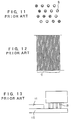
- FIGS. 6 and 7 show the screens at this time.
- FIG. 6 shows a good product, wherein the display of the both of the substrates is turned on every other line.
- FIG. 7 shows a defective product, wherein three lines are turned on consecutively. This method allows both substrates to be tested at the same time.
Landscapes
- Physics & Mathematics (AREA)
- Nonlinear Science (AREA)
- General Physics & Mathematics (AREA)
- Engineering & Computer Science (AREA)
- Crystallography & Structural Chemistry (AREA)
- Optics & Photonics (AREA)
- Chemical & Material Sciences (AREA)
- Liquid Crystal (AREA)
- Computer Hardware Design (AREA)
- Theoretical Computer Science (AREA)
- Mathematical Physics (AREA)
- Testing Of Short-Circuits, Discontinuities, Leakage, Or Incorrect Line Connections (AREA)
- Devices For Indicating Variable Information By Combining Individual Elements (AREA)
Applications Claiming Priority (2)
| Application Number | Priority Date | Filing Date | Title |
|---|---|---|---|
| JP7230252A JPH0980460A (ja) | 1995-09-07 | 1995-09-07 | 液晶表示装置及びその検査方法 |
| JP230252/95 | 1995-09-07 |
Publications (2)
| Publication Number | Publication Date |
|---|---|
| EP0762137A2 true EP0762137A2 (de) | 1997-03-12 |
| EP0762137A3 EP0762137A3 (de) | 1998-05-13 |
Family
ID=16904904
Family Applications (1)
| Application Number | Title | Priority Date | Filing Date |
|---|---|---|---|
| EP96306406A Withdrawn EP0762137A3 (de) | 1995-09-07 | 1996-09-04 | Flüssigkristallanzeige und Testverfahren dafür |
Country Status (4)
| Country | Link |
|---|---|
| EP (1) | EP0762137A3 (de) |
| JP (1) | JPH0980460A (de) |
| KR (1) | KR970016659A (de) |
| TW (1) | TW436654B (de) |
Cited By (9)
| Publication number | Priority date | Publication date | Assignee | Title |
|---|---|---|---|---|
| DE10227332A1 (de) * | 2002-06-19 | 2004-01-15 | Akt Electron Beam Technology Gmbh | Ansteuervorrichtung mit verbesserten Testeneigenschaften |
| US7319335B2 (en) | 2004-02-12 | 2008-01-15 | Applied Materials, Inc. | Configurable prober for TFT LCD array testing |
| US7330021B2 (en) | 2004-02-12 | 2008-02-12 | Applied Materials, Inc. | Integrated substrate transfer module |
| US7355418B2 (en) | 2004-02-12 | 2008-04-08 | Applied Materials, Inc. | Configurable prober for TFT LCD array test |
| US7535238B2 (en) | 2005-04-29 | 2009-05-19 | Applied Materials, Inc. | In-line electron beam test system |
| US7569818B2 (en) | 2006-03-14 | 2009-08-04 | Applied Materials, Inc. | Method to reduce cross talk in a multi column e-beam test system |
| US7602199B2 (en) | 2006-05-31 | 2009-10-13 | Applied Materials, Inc. | Mini-prober for TFT-LCD testing |
| US7786742B2 (en) | 2006-05-31 | 2010-08-31 | Applied Materials, Inc. | Prober for electronic device testing on large area substrates |
| CN111681545A (zh) * | 2020-05-27 | 2020-09-18 | 上海中航光电子有限公司 | 显示面板和显示装置 |
Families Citing this family (1)
| Publication number | Priority date | Publication date | Assignee | Title |
|---|---|---|---|---|
| KR100705630B1 (ko) * | 2004-12-31 | 2007-04-11 | 비오이 하이디스 테크놀로지 주식회사 | 액정표시장치의 어레이 테스트 방법 |
Family Cites Families (3)
| Publication number | Priority date | Publication date | Assignee | Title |
|---|---|---|---|---|
| JPH03223677A (ja) * | 1989-11-07 | 1991-10-02 | Sharp Corp | テスターヘッド |
| JPH05119336A (ja) * | 1991-10-30 | 1993-05-18 | Fujitsu Ltd | 液晶表示パネルの表示試験装置 |
| JPH05323357A (ja) * | 1992-05-15 | 1993-12-07 | Casio Comput Co Ltd | 基板の電極構造 |
-
1995
- 1995-09-07 JP JP7230252A patent/JPH0980460A/ja active Pending
-
1996
- 1996-09-04 EP EP96306406A patent/EP0762137A3/de not_active Withdrawn
- 1996-09-06 KR KR1019960038629A patent/KR970016659A/ko not_active Withdrawn
- 1996-09-06 TW TW085110915A patent/TW436654B/zh not_active IP Right Cessation
Cited By (13)
| Publication number | Priority date | Publication date | Assignee | Title |
|---|---|---|---|---|
| DE10227332A1 (de) * | 2002-06-19 | 2004-01-15 | Akt Electron Beam Technology Gmbh | Ansteuervorrichtung mit verbesserten Testeneigenschaften |
| US7847566B2 (en) | 2004-02-12 | 2010-12-07 | Applied Materials, Inc. | Configurable prober for TFT LCD array test |
| US7330021B2 (en) | 2004-02-12 | 2008-02-12 | Applied Materials, Inc. | Integrated substrate transfer module |
| US7355418B2 (en) | 2004-02-12 | 2008-04-08 | Applied Materials, Inc. | Configurable prober for TFT LCD array test |
| US7319335B2 (en) | 2004-02-12 | 2008-01-15 | Applied Materials, Inc. | Configurable prober for TFT LCD array testing |
| US7919972B2 (en) | 2004-02-12 | 2011-04-05 | Applied Materials, Inc. | Integrated substrate transfer module |
| US7535238B2 (en) | 2005-04-29 | 2009-05-19 | Applied Materials, Inc. | In-line electron beam test system |
| US7746088B2 (en) | 2005-04-29 | 2010-06-29 | Applied Materials, Inc. | In-line electron beam test system |
| US7569818B2 (en) | 2006-03-14 | 2009-08-04 | Applied Materials, Inc. | Method to reduce cross talk in a multi column e-beam test system |
| US7602199B2 (en) | 2006-05-31 | 2009-10-13 | Applied Materials, Inc. | Mini-prober for TFT-LCD testing |
| US7786742B2 (en) | 2006-05-31 | 2010-08-31 | Applied Materials, Inc. | Prober for electronic device testing on large area substrates |
| CN111681545A (zh) * | 2020-05-27 | 2020-09-18 | 上海中航光电子有限公司 | 显示面板和显示装置 |
| CN111681545B (zh) * | 2020-05-27 | 2022-03-29 | 上海中航光电子有限公司 | 显示面板和显示装置 |
Also Published As
| Publication number | Publication date |
|---|---|
| EP0762137A3 (de) | 1998-05-13 |
| KR970016659A (ko) | 1997-04-28 |
| JPH0980460A (ja) | 1997-03-28 |
| TW436654B (en) | 2001-05-28 |
Similar Documents
| Publication | Publication Date | Title |
|---|---|---|
| JP5057617B2 (ja) | 液晶表示装置及びその製造方法 | |
| US7507592B2 (en) | Bonding pad structure for a display device and fabrication method thereof | |
| US6835896B2 (en) | Packaging structure of a driving circuit for a liquid crystal display device and packaging method of a driving circuit for a liquid crystal display device | |
| EP1391774B1 (de) | Flüssigkristallanzeige | |
| KR100524033B1 (ko) | 전자 모듈 및 그 제조 방법 | |
| US20110102729A1 (en) | Flexible printed circuit and electric circuit structure | |
| JP3866815B2 (ja) | 液晶パネル用基板、その製造方法、液晶装置及び電子機器 | |
| JP2002090424A (ja) | マトリクスアレイ基板 | |
| KR100324283B1 (ko) | 테이프 캐리어 패키지 및 그 제조방법 | |
| US6300998B1 (en) | Probe for inspecting liquid crystal display panel, and apparatus and method for inspecting liquid crystal display panel | |
| KR20040059670A (ko) | 액정표시패널의 검사용 범프 구조 | |
| EP0762137A2 (de) | Flüssigkristallanzeige und Testverfahren dafür | |
| KR100293982B1 (ko) | 액정패널 | |
| US6806939B2 (en) | Display device | |
| JP3645172B2 (ja) | 半導体集積回路装置搭載用基板 | |
| US20030137629A1 (en) | Display device | |
| Masuda et al. | Chip on glass technology for large capacity and high resolution LCD | |
| JP3340005B2 (ja) | 液晶表示装置 | |
| JPH095381A (ja) | 液晶パネルと駆動回路素子の接続検査方法 | |
| Adachi | Packaging technology for liquid crystal displays | |
| JPH0643473A (ja) | 液晶表示装置 | |
| CN100480786C (zh) | 玻璃覆晶结构和采用该玻璃覆晶结构的液晶显示器 | |
| JPH10301138A (ja) | 液晶表示装置 | |
| JP2002246404A (ja) | バンプ付き半導体素子 | |
| JP2001005016A (ja) | 液晶装置及びその検査方法 |
Legal Events
| Date | Code | Title | Description |
|---|---|---|---|
| PUAI | Public reference made under article 153(3) epc to a published international application that has entered the european phase |
Free format text: ORIGINAL CODE: 0009012 |
|
| AK | Designated contracting states |
Kind code of ref document: A2 Designated state(s): DE FR GB |
|
| PUAL | Search report despatched |
Free format text: ORIGINAL CODE: 0009013 |
|
| AK | Designated contracting states |
Kind code of ref document: A3 Designated state(s): DE FR GB |
|
| STAA | Information on the status of an ep patent application or granted ep patent |
Free format text: STATUS: THE APPLICATION IS DEEMED TO BE WITHDRAWN |
|
| 18D | Application deemed to be withdrawn |
Effective date: 19981114 |