EP0755076B1 - Vertical MOS semiconductor with recessed gate and method of manufacturing the same - Google Patents
Vertical MOS semiconductor with recessed gate and method of manufacturing the same Download PDFInfo
- Publication number
- EP0755076B1 EP0755076B1 EP96107393A EP96107393A EP0755076B1 EP 0755076 B1 EP0755076 B1 EP 0755076B1 EP 96107393 A EP96107393 A EP 96107393A EP 96107393 A EP96107393 A EP 96107393A EP 0755076 B1 EP0755076 B1 EP 0755076B1
- Authority
- EP
- European Patent Office
- Prior art keywords
- semiconductor
- semiconductor layer
- semiconductor layers
- layers
- emitter
- Prior art date
- Legal status (The legal status is an assumption and is not a legal conclusion. Google has not performed a legal analysis and makes no representation as to the accuracy of the status listed.)
- Expired - Lifetime
Links
- 239000004065 semiconductor Substances 0.000 title claims description 290
- 238000004519 manufacturing process Methods 0.000 title claims description 33
- 239000010410 layer Substances 0.000 claims description 440
- 238000009413 insulation Methods 0.000 claims description 62
- 239000012535 impurity Substances 0.000 claims description 46
- 239000011229 interlayer Substances 0.000 claims description 38
- 239000000758 substrate Substances 0.000 claims description 18
- 238000000034 method Methods 0.000 claims description 13
- 239000004020 conductor Substances 0.000 claims 8
- 239000012774 insulation material Substances 0.000 claims 5
- 230000036961 partial effect Effects 0.000 description 34
- 230000003071 parasitic effect Effects 0.000 description 24
- 238000009792 diffusion process Methods 0.000 description 17
- 229910021420 polycrystalline silicon Inorganic materials 0.000 description 15
- 229920005591 polysilicon Polymers 0.000 description 15
- 230000003647 oxidation Effects 0.000 description 11
- 238000007254 oxidation reaction Methods 0.000 description 11
- 230000002829 reductive effect Effects 0.000 description 9
- 230000008569 process Effects 0.000 description 8
- 239000005380 borophosphosilicate glass Substances 0.000 description 7
- 238000005530 etching Methods 0.000 description 7
- 230000015572 biosynthetic process Effects 0.000 description 6
- 230000015556 catabolic process Effects 0.000 description 6
- XUIMIQQOPSSXEZ-UHFFFAOYSA-N Silicon Chemical compound [Si] XUIMIQQOPSSXEZ-UHFFFAOYSA-N 0.000 description 5
- 230000008859 change Effects 0.000 description 5
- 229910052710 silicon Inorganic materials 0.000 description 5
- 239000010703 silicon Substances 0.000 description 5
- 238000010586 diagram Methods 0.000 description 4
- 229910018125 Al-Si Inorganic materials 0.000 description 3
- 229910018520 Al—Si Inorganic materials 0.000 description 3
- 229910045601 alloy Inorganic materials 0.000 description 3
- 239000000956 alloy Substances 0.000 description 3
- 238000007796 conventional method Methods 0.000 description 3
- 238000002347 injection Methods 0.000 description 3
- 239000007924 injection Substances 0.000 description 3
- 230000002441 reversible effect Effects 0.000 description 3
- VYPSYNLAJGMNEJ-UHFFFAOYSA-N Silicium dioxide Chemical compound O=[Si]=O VYPSYNLAJGMNEJ-UHFFFAOYSA-N 0.000 description 2
- 238000000137 annealing Methods 0.000 description 2
- 230000003247 decreasing effect Effects 0.000 description 2
- 230000000694 effects Effects 0.000 description 2
- 230000005669 field effect Effects 0.000 description 2
- 230000000149 penetrating effect Effects 0.000 description 2
- 238000001020 plasma etching Methods 0.000 description 2
- 230000009467 reduction Effects 0.000 description 2
- ZOXJGFHDIHLPTG-UHFFFAOYSA-N Boron Chemical compound [B] ZOXJGFHDIHLPTG-UHFFFAOYSA-N 0.000 description 1
- OAICVXFJPJFONN-UHFFFAOYSA-N Phosphorus Chemical compound [P] OAICVXFJPJFONN-UHFFFAOYSA-N 0.000 description 1
- 229910052796 boron Inorganic materials 0.000 description 1
- 239000000969 carrier Substances 0.000 description 1
- 229910052681 coesite Inorganic materials 0.000 description 1
- 229910052906 cristobalite Inorganic materials 0.000 description 1
- 230000006378 damage Effects 0.000 description 1
- 230000001419 dependent effect Effects 0.000 description 1
- 238000005265 energy consumption Methods 0.000 description 1
- 238000005516 engineering process Methods 0.000 description 1
- 230000010354 integration Effects 0.000 description 1
- 230000002427 irreversible effect Effects 0.000 description 1
- 229910052698 phosphorus Inorganic materials 0.000 description 1
- 239000011574 phosphorus Substances 0.000 description 1
- 230000004044 response Effects 0.000 description 1
- 239000005368 silicate glass Substances 0.000 description 1
- 239000000377 silicon dioxide Substances 0.000 description 1
- 229910052682 stishovite Inorganic materials 0.000 description 1
- 229910052905 tridymite Inorganic materials 0.000 description 1
Images


Classifications
-
- H—ELECTRICITY
- H01—ELECTRIC ELEMENTS
- H01L—SEMICONDUCTOR DEVICES NOT COVERED BY CLASS H10
- H01L29/00—Semiconductor devices adapted for rectifying, amplifying, oscillating or switching, or capacitors or resistors with at least one potential-jump barrier or surface barrier, e.g. PN junction depletion layer or carrier concentration layer; Details of semiconductor bodies or of electrodes thereof ; Multistep manufacturing processes therefor
- H01L29/66—Types of semiconductor device ; Multistep manufacturing processes therefor
- H01L29/68—Types of semiconductor device ; Multistep manufacturing processes therefor controllable by only the electric current supplied, or only the electric potential applied, to an electrode which does not carry the current to be rectified, amplified or switched
- H01L29/76—Unipolar devices, e.g. field effect transistors
- H01L29/772—Field effect transistors
- H01L29/78—Field effect transistors with field effect produced by an insulated gate
-
- H—ELECTRICITY
- H01—ELECTRIC ELEMENTS
- H01L—SEMICONDUCTOR DEVICES NOT COVERED BY CLASS H10
- H01L29/00—Semiconductor devices adapted for rectifying, amplifying, oscillating or switching, or capacitors or resistors with at least one potential-jump barrier or surface barrier, e.g. PN junction depletion layer or carrier concentration layer; Details of semiconductor bodies or of electrodes thereof ; Multistep manufacturing processes therefor
- H01L29/02—Semiconductor bodies ; Multistep manufacturing processes therefor
- H01L29/06—Semiconductor bodies ; Multistep manufacturing processes therefor characterised by their shape; characterised by the shapes, relative sizes, or dispositions of the semiconductor regions ; characterised by the concentration or distribution of impurities within semiconductor regions
- H01L29/0684—Semiconductor bodies ; Multistep manufacturing processes therefor characterised by their shape; characterised by the shapes, relative sizes, or dispositions of the semiconductor regions ; characterised by the concentration or distribution of impurities within semiconductor regions characterised by the shape, relative sizes or dispositions of the semiconductor regions or junctions between the regions
- H01L29/0692—Surface layout
- H01L29/0696—Surface layout of cellular field-effect devices, e.g. multicellular DMOS transistors or IGBTs
-
- H—ELECTRICITY
- H01—ELECTRIC ELEMENTS
- H01L—SEMICONDUCTOR DEVICES NOT COVERED BY CLASS H10
- H01L29/00—Semiconductor devices adapted for rectifying, amplifying, oscillating or switching, or capacitors or resistors with at least one potential-jump barrier or surface barrier, e.g. PN junction depletion layer or carrier concentration layer; Details of semiconductor bodies or of electrodes thereof ; Multistep manufacturing processes therefor
- H01L29/02—Semiconductor bodies ; Multistep manufacturing processes therefor
- H01L29/06—Semiconductor bodies ; Multistep manufacturing processes therefor characterised by their shape; characterised by the shapes, relative sizes, or dispositions of the semiconductor regions ; characterised by the concentration or distribution of impurities within semiconductor regions
- H01L29/10—Semiconductor bodies ; Multistep manufacturing processes therefor characterised by their shape; characterised by the shapes, relative sizes, or dispositions of the semiconductor regions ; characterised by the concentration or distribution of impurities within semiconductor regions with semiconductor regions connected to an electrode not carrying current to be rectified, amplified or switched and such electrode being part of a semiconductor device which comprises three or more electrodes
- H01L29/1095—Body region, i.e. base region, of DMOS transistors or IGBTs
-
- H—ELECTRICITY
- H01—ELECTRIC ELEMENTS
- H01L—SEMICONDUCTOR DEVICES NOT COVERED BY CLASS H10
- H01L29/00—Semiconductor devices adapted for rectifying, amplifying, oscillating or switching, or capacitors or resistors with at least one potential-jump barrier or surface barrier, e.g. PN junction depletion layer or carrier concentration layer; Details of semiconductor bodies or of electrodes thereof ; Multistep manufacturing processes therefor
- H01L29/66—Types of semiconductor device ; Multistep manufacturing processes therefor
- H01L29/66007—Multistep manufacturing processes
- H01L29/66075—Multistep manufacturing processes of devices having semiconductor bodies comprising group 14 or group 13/15 materials
- H01L29/66227—Multistep manufacturing processes of devices having semiconductor bodies comprising group 14 or group 13/15 materials the devices being controllable only by the electric current supplied or the electric potential applied, to an electrode which does not carry the current to be rectified, amplified or switched, e.g. three-terminal devices
- H01L29/66234—Bipolar junction transistors [BJT]
- H01L29/66325—Bipolar junction transistors [BJT] controlled by field-effect, e.g. insulated gate bipolar transistors [IGBT]
- H01L29/66333—Vertical insulated gate bipolar transistors
- H01L29/66348—Vertical insulated gate bipolar transistors with a recessed gate
-
- H—ELECTRICITY
- H01—ELECTRIC ELEMENTS
- H01L—SEMICONDUCTOR DEVICES NOT COVERED BY CLASS H10
- H01L29/00—Semiconductor devices adapted for rectifying, amplifying, oscillating or switching, or capacitors or resistors with at least one potential-jump barrier or surface barrier, e.g. PN junction depletion layer or carrier concentration layer; Details of semiconductor bodies or of electrodes thereof ; Multistep manufacturing processes therefor
- H01L29/66—Types of semiconductor device ; Multistep manufacturing processes therefor
- H01L29/68—Types of semiconductor device ; Multistep manufacturing processes therefor controllable by only the electric current supplied, or only the electric potential applied, to an electrode which does not carry the current to be rectified, amplified or switched
- H01L29/70—Bipolar devices
- H01L29/72—Transistor-type devices, i.e. able to continuously respond to applied control signals
- H01L29/739—Transistor-type devices, i.e. able to continuously respond to applied control signals controlled by field-effect, e.g. bipolar static induction transistors [BSIT]
- H01L29/7393—Insulated gate bipolar mode transistors, i.e. IGBT; IGT; COMFET
- H01L29/7395—Vertical transistors, e.g. vertical IGBT
- H01L29/7396—Vertical transistors, e.g. vertical IGBT with a non planar surface, e.g. with a non planar gate or with a trench or recess or pillar in the surface of the emitter, base or collector region for improving current density or short circuiting the emitter and base regions
- H01L29/7397—Vertical transistors, e.g. vertical IGBT with a non planar surface, e.g. with a non planar gate or with a trench or recess or pillar in the surface of the emitter, base or collector region for improving current density or short circuiting the emitter and base regions and a gate structure lying on a slanted or vertical surface or formed in a groove, e.g. trench gate IGBT
-
- H—ELECTRICITY
- H01—ELECTRIC ELEMENTS
- H01L—SEMICONDUCTOR DEVICES NOT COVERED BY CLASS H10
- H01L2924/00—Indexing scheme for arrangements or methods for connecting or disconnecting semiconductor or solid-state bodies as covered by H01L24/00
- H01L2924/0001—Technical content checked by a classifier
- H01L2924/0002—Not covered by any one of groups H01L24/00, H01L24/00 and H01L2224/00
Definitions
- the present invention relates to an insulated gate semiconductor device and a method of manufacturing the same. More particularly, the present invention relates to a device structure in which a parasitic transistor of an insulated gate bipolar transistor which comprises a trench MOS gate does not turn on easily so that an safe operating area (hereinafter "SOA") is large, and also relates to a method of manufacturing the same.
- SOA safe operating area
- Fig. 26 is a partial sectional view of a conventional insulated gate semiconductor device.
- an insulated gate bipolar transistor hereinafter "IGBT"
- an IGBT having a trench gate structure An IGBT having a trench gate structure will be hereinafter referred to as a “U-type IGBT."
- IGBTs have been very often used in various devices such as an intelligent power module which controls a variable speed of a tri-phase motor, to reduce energy consumption, the size and the weight of electric household appliances. While a switching characteristic, a saturation voltage and an SOA are in a trade-off relationship with each other in IGBTs, i.e., key devices in these various devices, IGBTs with a better switching characteristic, a low saturation voltage and a large SOA are demanded.
- Fig. 26 denoted at 1 is a P + collector layer, denoted at 2 is an N - layer, denoted at 3 is a P base layer, denoted at 4 are N + emitter regions, denoted at 5 are trenches, denoted at 6 are gate insulation films, denoted at 7 are gate electrodes, denoted at 8 is an interlayer insulation film, denoted at 9 is an N + buffer layer, denoted at 10 is an emitter electrode, denoted at 11 is a collector electrode, and denoted at 12 are channel regions.
- the gate voltage V GE applied across the emitter electrode 10 and the gate electrodes 7 is changed to 0V or a reverse bias is applied across the emitter electrode 10 and the gate electrodes 7, thereby turning the gates off.
- the channel regions 12 inverted into the N type return to the P type so that injection of electrons from the emitter electrode 10 stops. Electrons and holes accumulated in the N - layer 2 then flow into the collector electrode 11 and the emitter electrode 10, respectively, or recombine with each other to perish.
- the ON-voltage of the IGBT is primarily determined by a substantial resistance of the N - layer 2 which is necessary to hold a breakdown voltage.
- One of the factors which determines the substantial resistance is an ability of a MOSFET which forms the IGBT to supply electrons.
- a cut-off current value under an applied high voltage is an important electric characteristic of an IGBT. It is therefore preferable to ensure as high cut-off current value as possible.
- the U-type IGBT includes a parasitic bipolar transistor which is formed by the N + emitter regions 4, the P base layer 3 and the N - layer 2.
- the gate voltage V GE alone can not control a current which flows in the U-type IGBT any more, whereby the U-type IGBT is destroyed.
- various device structures have been proposed in which the cell size is small, using a trench gate structure so that the parasitic bipolar transistor does not easily turn on.
- Fig. 27 is a partial sectional view showing an example of a conventional insulated gate semiconductor device which is described in Japanese Patent Unscreened Publication No. 60-253275.
- Fig. 27 denoted at 13 is a semiconductor substrate, denoted at 14 is a first major surface of the semiconductor substrate 13, and denoted at 15 are P + regions.
- the other reference symbols are similar to those used in Fig. 24.
- the P + regions 15 of the N + emitter regions 4 are disposed simply to ensure a better contact with the emitter electrode 10.
- the impurity concentration of the P + regions 15 is lower than that of the N + emitter regions.
- Fig. 28 is a schematic diagram showing a contact margin in the conventional technique.
- the gate electrodes 7 are trench type electrodes rather than V-shaped electrodes.
- Fig. 28 shows additional areas which are necessary for the N + emitter regions 4 to deal with misalignment of the masks (i.e., gate contact margins).
- Fig. 29 is a partial sectional view showing an example of a conventional insulated gate semiconductor device which is described in USP No. 5,034,785.
- the intervals between cells are shorter in the illustrative device since the illustrative device does not use the gate contact margins which are used in the conventional technique of Fig. 28.
- the device shown in Fig. 29 is a DMOS power transistor, and includes a gate of a trench structure.
- the gate electrodes 7 has a surface which is recessed from the first major surface 14 of the semiconductor substrate 13.
- Denoted at 16 is a source electrode.
- the surfaces of the gate electrodes 7 is recessed from the first major surface 14 of the semiconductor substrate 13. This makes a mask unneeded to form the gate electrodes 7 and makes it unnecessary for the source electrode to have a margin for alignment of the masks. Hence, it is possible to reduce the trench pitch.
- the N + source region 16 is formed deeper than the surfaces of the gate electrodes 7.
- the N + source region 16 therefore tends to be deeper. Since the N + source region 16 is formed by diffusion in most cases, when the N + source region 16 is diffused deep, the N + source region 16 is diffused wide. This increases the trench pitch.
- Fig. 30 is a schematic diagram showing side diffusion in the conventional structure.
- the illustrative device is an IGBT.
- the N + emitter regions 4 are formed deeper and therefore side diffusion of the N + emitter regions 4 is large.
- the trench pitch must be formed large. This allows the parasitic transistor to easily turn on.
- I C (sat) The value of a current which flows in an IGBT in response to a certain applied gate voltage is expressed as I C (sat). If the value I C (sat) is too large, the parasitic transistor easily turns on, which in turn destroys the IGBT.
- JP-A-1198076 discloses a semiconductor device for enabling the increase of latch-up yield strength. by forming trench to reduce a first conductivity type base on the source side of a vertical gate structure IGBT, and forming a source electrode stretching as far as the trench bottom, or installing, instead of the trench, a first conductivity type diffusion region of high impurity concentration.
- the source side surface of a vertical gate structure IGBT is flattened, and the source side surface except the exposed region of a P + base layer is covered with a resist film.
- a second trench is dug, the surface side region of the P + base layer is shaved off.
- the resist film is eliminated, and a source electrode stretching as far as the side surface and the bottom surface of the second trench is formed.
- a drain electrode is formed, and polysilicon is buried in the second trench to complete a semiconductor device.
- a P ++ high concentration diffusion region of low resistance is installed instead of the trench, and the series resistance component between the P + base layer and the source electrode is reduced. Thereby, latch-up yield strength can be improved.
- JP-A-6350071 discloses a longitudinal type MOS field effect transistor in which a pattern pitch is extremely miniaturized, integration density is increased, and miniaturization of a chip is realized and reduction of an ON-resistance is possible by forming a short-circuit between a source region and a diffusion region for a channel with a source electrode.
- a P-type region for a channel is formed, and then a mesh-shaped N + type region for a source is formed in a plane in the manner in which a region appears here and there on the surface. Further, an U-shaped groove is formed, and a gate oxide film is formed.
- a window for forming an electrode with the same width as that of the mesh of the N + -type region for a mesh-shaped source is formed. After that, an electrode for a gate, an electrode for a source, and an electrode for a drain are formed.
- EP-A-68945 discloses a bipolar transistor controlled by field effect by means of an isolated gate in which a bipolar semiconductor structure, the conductive and blocked states of which are controlled by an isolated gate comprises a P + type substrate constituting the emitter of a bipolar transistor, an N type epitaxial layer constituting the base, a P + type area having a large surface, constituting a collector, covered with a collector contact and surrounded by an area wherein the epitaxial N type layer is exposed, an N + type source area included in the collector area and extending along the border of the same so as to define an interval which constitutes the control gate of the structure, a resistive source access zone connected, on the one hand, to the source, and on the other hand, to the collector contact, the resistance of this zone being sufficient for preventing the structure from being rendered conductive in an irreversible manner.
- US-A-5,169,793 discloses a method of manufacturing an insulated gate bipolar transistor having a gate shielded region in which a p type pad well layer is formed at the surface of an n - type drain layer under a gate bonding pad and the surface thereof is provided with a p ++ type pad layer to be provided with lower resistivity.
- the p ++ type pad layer is connected with a source electrode through a contact hole. Since the gate electrode supplying each cell with gate potential is of a pattern having extensions in a comb-teeth form arranged along the boundary between the pad region and the cell region, there is present substantially no gate electrode under the pad.
- the introduction of impurities into the entire surface of the well layer under the pad region can be performed simultaneously with formation of p ++ type contact layers after the formation of the gate electrode, and accordingly, the low resistance p ++ type pad layer can be easily formed.
- the p ++ type pad layer serves as a low resistance path for allowing the holes flowing into the region under the pad region of the insulated gate bipolar transistor to escape to the source electrode, whereby occurrence of latch-up and an increase in the turn-off time due to the minority carriers concentrating into the border portion cell located adjacent to the pad region can be prevented.
- an object of the present invention to provide for an insulated gate semiconductor device which has a device structure in which a parasitic transistor does not easily turn on and therefore the SOA is improved, and a method of manufacturing such a device.
- the present invention provides an insulated gate semiconductor device as reflected in independent claim 1 as well as a method of manufacturing an insulated gate semiconductor device as reflected in independent claim 7.
- Preferred embodiments of the invention are reflected in the dependent claims.
- the fifth semiconductor layer is disposed on the surfaces of the third and the fourth semiconductor layers to extend across the third and the fourth semiconductor layers, a junction between the fifth and the fourth semiconductor layers is exposed to a surface, and the bottom surface of the fifth semiconductor layer is located at a shallower position than the thickness of the fourth semiconductor layer. Therefore, even when the exposed surface of the third semiconductor layer which is adjacent to the fourth semiconductor layer becomes small, since the first major electrode creates a contact between the third and the fourth semiconductor layers through the fifth semiconductor layer, the cell size remains small, the ON-voltage is reduced, a parasitic transistor does not easily turn on, and the value of a current which can be terminated at turning off does not drop. Hence, the insulated gate semiconductor device uses small consumption power, an RBSOA of the insulated gate semiconductor device is large, and the reliability of the insulated gate semiconductor device is high.
- the exposed surface of the fifth semiconductor layer is formed between adjacent inner walls, and the exposed surface extends along the inner walls in the direction of the longitudinal extension of the inner walls, it is possible to form a plurality of the control electrodes. Further, even when adjacent fourth semiconductor layers are extremely close to each other through the exposed surface of the fifth semiconductor layer, the first major electrode creates a contact between the third and the fourth semiconductor layers through the fifth semiconductor layer.
- trench intervals are small and the device is small and dense.
- the exposed surface of the fifth semiconductor layer has a scattered configuration
- the link portion of the fourth semiconductor layer which separates the exposed surface portions of the fifth semiconductor layer which are located between adjacent inner walls, the first major electrode creates a contact between the third and the fourth semiconductor layers. Therefore, trench intervals are small in the insulated gate semiconductor device, and the insulated gate semiconductor device is small and dense.
- the film covers the inner walls, the portions of the surfaces of the fourth semiconductor layers which are adjacent to each other along the inner walls and the portions of the surfaces of the fifth semiconductor layers which are adjacent to the portions of the fourth semiconductor layers, the link portions of the fourth semiconductor layers, which separate the fifth semiconductor layers which are located between adjacent inner walls, and the fifth semiconductor layers alternately contact the first major electrode, but the fourth semiconductor layers which are sandwiched by the fifth semiconductor layers and the inner walls do not contact the first major electrode.
- these portions serve as a resistance between the fourth semiconductor layers which contact the first major electrode. When a large current flows, the resistance induces a voltage drop within the fourth semiconductor layers.
- a parasitic transistor does not easily turn on in the insulated gate semiconductor device, an RBSOA of the insulated gate semiconductor device is large, the insulated gate semiconductor device is small and dense, and the reliability of the insulated gate semiconductor device is high.
- the fourth semiconductor layers sandwich the fifth semiconductor layer in the form of columns, the plurality of the inner walls are formed along this column-like arrangement, the interlayer insulation film is formed on the surface of the control electrode, and the first major electrode is disposed on the surfaces of the fourth and the fifth semiconductor layers and the interlayer insulation film, it is possible to form a plurality of the control electrodes. It is also possible to form the exposed surface of the fifth semiconductor layer small. Even without creating the additional area to the interlayer insulation film for the sake of aligning a mask, the first major electrode creates a contact between the third and the fourth semiconductor layers through the fifth semiconductor layer. This reduces trench intervals and the cell size.
- the insulated gate semiconductor device uses small consumption power, an RBSOA of the insulated gate semiconductor device is large, the reliability of the insulated gate semiconductor device is high, and the insulated gate semiconductor device is small and dense.
- the link portion of the fourth semiconductor layer which separates exposed surface portions of the fifth semiconductor layer which are located between adjacent inner walls is not coated with the interlayer insulation film. This link portion of the fourth semiconductor layer allows the first major electrode to create a contact between the third and the fourth semiconductor layers.
- the insulated gate semiconductor device has even smaller trench intervals, a small size and a high density.
- the insulation film may cover those fourth semiconductor layers which are adjacent to each other along the wall surfaces and the portion of the fifth semiconductor layer which is in the vicinity of those fourth semiconductor layers.
- the link portions of the fourth semiconductor layers, which separate the fifth semiconductor layer into the scattered configuration, and the fifth semiconductor layer alternately contact the first major electrode. Since the fourth semiconductor layers which are sandwiched between the fifth semiconductor layer and the inner walls do not contact the first major electrode in this configuration, these portions serve as a resistance between the fourth semiconductor layers which contact the first major electrode. When a large current flows, the resistance induces a voltage drop within the fourth semiconductor layers.
- a parasitic transistor does not easily turn on in the insulated gate semiconductor device, and an RBSOA of the insulated gate semiconductor device is large. Further, the breakdown characteristic during shorting is improved without increasing the cell size.
- the insulated gate semiconductor device is small and dense, and the reliability of the insulated gate semiconductor device is high.
- the first major electrode creates a contact between the third and the fourth semiconductor layers through the fifth semiconductor layer.
- an insulated gate semiconductor device which uses small consumption power, which has a large RBSOA and which is highly reliable, at an inexpensive cost without complex manufacturing steps.
- an insulated gate semiconductor device in which an additional area to the interlayer insulation film for the sake of aligning a mask is small, cell intervals are small, consumption power is small, an RBSOA is large, and the reliability is high, at an inexpensive cost without complex manufacturing steps.
- the interlayer insulation film does not cover the link portions of the fourth semiconductor layers, which separate the exposed surface of the fifth semiconductor layer which are located between adjacent inner walls, and the link portions of the fourth semiconductor layers and the fifth semiconductor layer allow the first major electrode to create a contact between the third and the fourth semiconductor layers, it is possible to manufacture an insulated gate semiconductor device in which cell intervals are small, at an inexpensive cost without complex manufacturing steps.
- the fourth semiconductor layers which are sandwiched between the fifth semiconductor layer and the inner walls serve as a resistance between the fourth semiconductor layers which contact the first major electrode.
- the resistance induces a voltage drop within the fourth semiconductor layers.
- Fig. 1 denoted at 30 is a U-type IGBT, denoted at 31 is an emitter electrode which functions as a first major electrode, denoted at 32 are gate lines, denoted at 33 is a gate pad, and denoted at 34 is a part of cells.
- Figs. 2 and 3 denoted at 41 is a P + collector layer which serves as a first semiconductor layer, denoted at 42 is an N - layer which serves as a second semiconductor layer, denoted at 43 is a P base layer which serves as a third semiconductor layer, denoted at 44 are N + emitter layers which serve as a fourth semiconductor layer, denoted at 45 are P + semiconductor layers which serve as a fifth semiconductor layer, denoted at 46 is an N + buffer layer, denoted at 47 are inner walls each formed in the shape of a groove. Trenches are defined by the inner walls 47.
- Denoted at 48 are gate insulation films, denoted at 49 are gate electrodes each serving as a control electrode, denoted at 50 is the interlayer insulation film, and denoted at 51 is the emitter electrode which serves as the first major electrode.
- the emitter electrode 51 is a portion of the emitter electrode 31 of Fig. 1.
- Denoted at 52 is a collector electrode which serves as a second major electrode, and denoted at 53 are channel regions. Areas C defined by brackets and dashed-and-dotted lines in Fig. 2 are areas which are covered with the interlayer insulation film 50.
- the gate insulation films 48 are thermal oxidation films of SiO 2
- the gate electrodes 49 are made of polysilicon doped with N-type impurities.
- the interlayer insulation film 50 is made of silicate glass containing boron and phosphorus (hereinafter "BPSG").
- the emitter electrode 51, the gate lines 32 and the gate pad 33 are made of Al containing Si (hereinafter "Al-Si”).
- the collector electrode 52 is made of AlMoNiAu alloy.
- the gate lines 32 are connected to the gate electrodes 49 so that polysilicon portions in paths from the gate electrodes 49 to the gate pad 33 are small so that an electric resistance from the gate electrodes 49 to the gate pad 33 is reduced and so that the element is controlled uniformly over the entire surface of the element.
- the N + buffer layer 46 is disposed on a surface of the P + collector layer 41, and the N - layer 42 is disposed on a surface of the N + buffer layer 46. Further, the P base layer 43 is disposed on the N - layer 42.
- the N + emitter layers 44 are disposed on a surface of the P base layer 43 at intervals so as to form stripes. Along the longitudinal extension of the stripes of the N + emitter layers 44, the trench-shaped inner walls 47 are formed, extending from surfaces of the N + emitter layers 44 and penetrating into the N - layer 42 through the P base layer 43.
- the P + semiconductor layers 45 are formed in such a manner that bottom surfaces of the P + semiconductor layers 45 contact the P base layer 43, and partially overlap the N + emitter layers 44 at the both ends, and that junctions between the N + emitter layers 44 and the P + semiconductor layers 45 are exposed to a surface.
- the impurity concentration of the P + semiconductor layers 45 is generally higher than that of the N + emitter layers 44. If the impurity concentration of the N + emitter layers 44 is set at about 1 ⁇ (10 18 - 10 19 ), the impurity concentration of the P + semiconductor layers 45 is set around 2 ⁇ (10 18 - 10 19 ), i.e., about twice higher than the impurity concentration of the N + emitter layers 44.
- the gate insulation films 48 are disposed in the inner walls 47.
- the gate insulation films 48 extend up to the surfaces of the N + emitter layers 44 which are adjacent to openings 56 of the inner walls 47.
- each gate electrode 49 is filled in up to each opening at the surfaces of the N + emitter layers 44.
- Surfaces of the gate electrodes 49 are lower than surfaces of the gate insulation films 48 which are formed on the surfaces of the N + emitter layers 44 which are adjacent to the openings 56 of the inner walls 47.
- the surfaces of the gate electrodes 49 are flush with the surfaces of the N + emitter layers 44. Although the surfaces of the gate electrodes 49 may be further recessed from the surfaces of the N + emitter layers 44, to form channels, the surfaces of the gate electrodes 49 must be located at a shallower position than the bottom of the N + emitters layers 44.
- the gate electrodes 49 are faced with the surfaces of the P base layer 43 through the gate insulation films 48. The surfaces of the P base layer 43 serves as the channel regions 53.
- the surfaces of the gate electrodes 49 are covered with the interlayer insulation film 50.
- the emitter electrode 51 is disposed on a surface of the element in which the N + emitter layers 44 and the P + semiconductor layers 45 are formed.
- the N + emitter layers 44 and the P base layer 43 contact the emitter electrode 51 through the P + semiconductor layers 45.
- the gate lines 32 and the gate pad 33 which are connected to the gate electrodes 49 are disposed on the surface of the element, while insulated from the N + emitter layers 44 and the P + semiconductor layers 45.
- the collector electrode 52 is disposed on the other surface of the P + collector layer 41.
- the element has a breakdown voltage on the order of 2,000 V, for example, the thickness from the surface of the element, i.e., the exposed surfaces of the P + semiconductor layers 45, or from the surfaces of the N + emitter layers 44 to a boundary between the N - layer 42 and the N + buffer layer 46 is about 200 ⁇ m, the impurity concentration of the N - layer 42 is 5 ⁇ 10 13 cm -3 , the intervals between the trench-shaped inner walls 47, i.e., the intervals between the cells are about 4 ⁇ m, and the depth of the inner walls 47 measured from the surfaces of the P + semiconductor layers 45 is about 8 ⁇ m.
- the depth of a junction between bottom surfaces of the N + emitter layers 44 and the P base layer 43 is about 1 ⁇ m, either from the N + emitter layers 44 or from the surfaces of the P + semiconductor layers 45.
- the thickness of the N + buffer layer 46 is about 10 ⁇ m, and the thickness of the P + collector layer 41 is about 300 ⁇ m.
- the gate voltage V GE applied across the emitter electrode 51 and the gate electrodes 49 is changed to 0V or a reverse bias is applied across the emitter electrode 51 and the gate electrodes 49, thereby turning the gates off.
- the channel regions 53 inverted into the N type return to the P type so that injection of electrons from the emitter electrode 51 stops and injection of holes from the P + collector layer 41 into the N - layer 42 stops. Electrons and holes accumulated in the N - layer 42 then flow into the collector electrode 52 and the emitter electrode 51, respectively, or recombine with each other to perish. Since holes can easily move within the P + semiconductor layers 45 at this stage, the switching speed becomes faster.
- Fig. 4 is a schematic partial cross sectional view showing the present invention.
- Fig. 4 describes an effect of the P + semiconductor layers 45 in the present invention.
- the surfaces of the gate electrodes 49 are located at about half the depth of the N + emitter layers 44, measured from the surfaces of the N + emitter layers 44.
- the thickness of the N + emitter layers 44 needs be large. Since the N + emitter layers 44 are formed by diffusion in most cases, when the N + emitter layers 44 are formed thick, due to side diffusion, adjacent edge portions of the N + emitter layers 44 which are disposed between adjacent trench-shaped inner walls 47 are positioned extremely close to each other.
- the adjacent edge portions of the N + emitter layers 44 are positioned close to each other, or even may contact each other in some cases. However, even if the adjacent edge portions of the N + emitter layers 44 contact each other, since the P + semiconductor layers 45 penetrating the N + emitter layers 44 contact the P base layer 43, the P base layer 43 and the N + emitter layers 44 contact the emitter electrode 51 through the P + semiconductor layers 45.
- the impurity concentration of the N + emitter layers 44 must be higher than that of the P base layer 43. Further, since the P + semiconductor layers 45 are diffused so as to overlap adjacent edge portions of the N + emitter layers 44, the impurity concentration of the P + semiconductor layers 45 must be higher than that of the N + emitter layers 44.
- the P + semiconductor layers 45 are formed first and the N + emitter layers 44 are then formed to have a higher impurity concentration than that of the P + semiconductor layers 45, adjacent edge portions of the N + emitter layers 44 come close to each other. As a result, the P + semiconductor layers 45 are eliminated by the N + emitter layers 44 in the present embodiment, and therefore, the effect of disposing the P + semiconductor layers 45 in the first preferred embodiment is not created.
- Fig. 5 is a graph showing a relationship between the trench pitch and the ON-voltage in the U-type IGBT.
- the P + semiconductor layers 45 are formed so as to overlap adjacent edge portions of the N + emitter layers 44 and so as to contact the P base layer 43, the emitter electrode 51 and the P base layer 43 contact each other through the P + semiconductor layers 45. As a result, the trench pitch and hence the ON-voltage are reduced. Further, the element becomes smaller and denser and the reliability is improved.
- the parasitic transistor which is formed by the N + emitter regions 4, the P base layer 3 and the N - layer 2 does not easily turn on.
- the parasitic bipolar transistor when holes flow into the emitter electrode 10, if the cell size is small, the quantity of holes which flow into one cell becomes small. Since the hole current serves as a base current of the parasitic bipolar transistor, if the potential of the P base layer 3 exceeds a built-in potential (0.6 V, in general) between the P base layer 3 and the N + emitter regions 4, the parasitic bipolar transistor turns on.
- Figs. 6 to 14 are partial cross sectional views showing the element during the respective stages of manufacturing.
- N + layer 61 and an N - layer 62 are epitaxially grown on P + silicon substrate 60, successively.
- P-type impurities are implanted and annealed in a surface of the N - layer 62, whereby a P base layer 63 is defined (See Fig. 6).
- a resist is stacked on a surface of the P base layer 63, and through photolithographic processes, a resist pattern 64 which includes a plurality of strip-shaped openings is formed.
- the surface of the P base layer 63 is doped with N-type impurities to a high concentration.
- the resist pattern 64 is thereafter removed.
- the impurities are annealed and diffused to define N + emitter regions 65 (See Fig. 7).
- An oxide film 66 which serves as a shielding film is then formed on a surface of the P base layer 63 and the N + emitter regions 65.
- a silicon etching mask is formed which includes a strip-like shaped opening which has a narrower width than the N + emitter regions 65, using the oxide film 66.
- RIE reactive Ion Etching
- a thermal oxidation film 68 which serves as an insulation film is formed on surfaces of the inner walls 67, a surface of the P base layer 63 and the surfaces of the N + emitter regions 65.
- Electrically conductive polysilicon 69 doped with N-type impurities is stacked on the thermal oxidation film 68, whereby the grooves formed by the inner walls 67 are filled up (See Fig. 9).
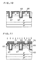
- the stacked polysilicon 69 is then etched back so that a surface of the polysilicon 69 filling up the grooves formed by the inner walls 67 is recessed from a surface of the thermal oxidation film 68 which is formed on the surfaces of the N + emitter regions 65 (See Fig. 10). Etching back must be performed so that the surface of the polysilicon 69 is positioned at a shallower position than the bottom of the N + emitter regions 65.
- a resist 70 is then stacked on the surface of the polysilicon 69 filling up the grooves formed by the inner walls 67 and on the surface of the thermal oxidation film 68.
- an opening is formed by photolithographic processes to surround the surface of the P base layer 63 and portions of the N + emitter regions 65 which are adjacent to the P base layer 63 and which extend along the inner walls 67, whereby a resist pattern is obtained.
- P-type impurities are implanted through the thermal oxidation film 68, at a higher impurity concentration than that of the N + emitter regions 65.
- the resist pattern is thereafter removed.
- the P-type impurities are diffused shallower than the bottom of the N + emitter regions 65, to define a P + semiconductor layer 71 whose bottom surface contacts the P base layer 63 (See Fig. 11).
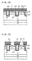
- a BPSG 72 which serves as an insulation is stacked on the surface of the polysilicon 69 filling up the grooves formed by the inner walls 67 and on the surface of the thermal oxidation film 68 (See Fig. 12).
- a resist 73 is stacked on a surface of the BPSG 72.
- an opening is formed by photolithographic processes which surrounds the P + semiconductor layer 71 and portions of the N + emitter regions 65 which are adjacent to the P + semiconductor layer 71 and which extend along the inner walls 67, whereby a resist pattern is obtained.
- the BPSG 72 and the thermal oxidation film 68 are etched so that an interlayer insulation film 72 is formed on the surface of the polysilicon 69 filling up the grooves formed by the inner walls 67 (See Fig. 13). The resist pattern is thereafter removed.
- Al-Si is stacked which serves as a conductive layer on a surface of the element in which the P + semiconductor layer 71, the N + emitter regions 65 and the interlayer insulation film 72 are formed. This creates a gate line and a gate pad at the same time which are connected to the polysilicon 69 which is buried in the grooves which are defined by the emitter electrode 73 and the inner walls 67 (See Fig. 14).
- AlMoNiAu alloy which serves as a conductive layer is stacked on the surface of the P + silicon substrate 60, thereby forming a collector electrode 75.
- the U-type IGBT is manufactured at an inexpensive cost.
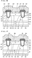
- Fig. 15 is a partial plan view of an insulated gate semiconductor device according to an embodiment of the present invention
- Fig. 16 is a partial cross sectional view of some cells of Fig. 15 taken along lines A-A
- Fig. 17 is a partial cross sectional view of some cells of Fig. 15 taken along lines B-B.
- the cells are shown as they are with the emitter electrode 51 and the interlayer insulation film 50 removed.
- Areas C defined by brackets and dashed-and-dotted lines in Fig. 15 are areas which are covered with the interlayer insulation film 50.
- the N + emitter layers 44 which are formed between the groove-shaped inner walls 47 have a ladder-like plan configuration.
- the N + emitter layers 44 are arranged in the shape of strips, sandwiching the exposed surfaces of the P + semiconductor layers 45.
- the groove-shaped inner walls 47 including openings at the surfaces of the N + emitter layers 44 extend along the longitudinal direction of the N + emitter layers 44.
- Adjacent N + emitter layers 44 which are disposed between the gate electrodes 49 which are buried in the inner walls are connected to each other through link portions 55.
- the exposed surfaces of the P + semiconductor layers 45 and the link portions 55 are disposed alternately.
- the area C of the interlayer insulation film 50 covers the gate electrodes 49 and extends over adjacent N + emitter layers 44 which are adjacent to and along the groove-shaped inner walls 47, but does not extend over the exposed surfaces of the P + semiconductor layers 45.
- the illustrative U-type IGBT is otherwise similar in structure to the U-type IGBT according to Fig. 3.
- the plan configuration of the N + emitter layers 44 is a ladder-like configuration, a contact area at which the emitter electrode 51 contacts the N + emitter layers 44 is ensured by the link portions 55 as well, which eliminates the necessity to additionally create an additional contact area to deal with misalignment of masks. That is, since it is not necessary to ensure an additional area to deal with misalignment of masks when the emitter electrode 73 shown in Fig. 13 is formed and since the cell intervals can be reduced accordingly, as compared in the structure in which the N + emitter layers 44 are disposed simply to extend along the gate electrodes 49 as shown in Fig. 2, it is possible for the cells to have fine geometry. Further, it is possible to arrange contact areas in a good balance all over the element.
- the element is formed denser and to have a low ON-voltage. It is possible to unify operation characteristics of the respective cells all over the element.
- the P + semiconductor layers 45 are not formed, and the exposed surfaces of the P base layer 43 is simply formed, the thicker the N + emitter layers 44 become, the wider the link portions 55 of the N + emitter layers 44 become due to diffusion in the horizontal direction, whereby the quantity of a hole current which flows immediately below the link portions 55 becomes large. Since the holes serve as a base current for the parasitic transistor which is formed by the N + emitter regions 44, the P base layer 43 and the N - layer 42, the parasitic transistor is easily turned on. However, since the P + semiconductor layers 45 are disposed which restrict the diffusion of the link portions 55 in the direction of the width of the link portions 55, the parasitic transistor does not tend to turn on. Hence, it is possible to prevent a reduction of the RBSOA.
- the manufacturing processes according to the present embodiment use a different resist pattern to form the N + emitter regions 65.
- the resist is stacked on the surface of the P base layer 63, the plurality of the openings which are in the shape of parallel strips and the openings which are linked to these openings are formed by photolithographic processes, the resist pattern in which resists are left scattered in the shape of columns is formed, and using this resist pattern 64 as a mask, N-type impurities are implanted into the surface of the P base layer 63 at a high doping concentration and diffused by annealing to thereby define the N + emitter regions 65.
- the P + semiconductor layers 71 are formed using a resist pattern which has a different shape.
- a resist openings are formed in correspondence with the exposed surfaces of the P base layers 63 which are formed on the N + emitter regions 65 in a scattered configuration.
- impurities are implanted and then diffused by thermal processing, to thereby define the P + semiconductor layers 71.
- Fig. 18 is a partial plan view of a U-type IGBT according to an alternative configuration not covered by the scope of the present invention
- Fig. 19 is a partial cross sectional view of some cells of Fig. 18 taken along lines A-A
- Fig. 20 is a partial cross sectional view of some cells of Fig. 18 taken along lines B-B.
- the cells are shown as they are with the emitter electrode 51 and the interlayer insulation film 50 removed.
- Areas C defined by brackets and dashed-and-dotted lines in Fig. 18 are areas which are covered with the interlayer insulation film 50.
- the N + emitter layers 44 which are formed between the groove-shaped inner walls 47 have a ladder-like plan configuration.
- the P + semiconductor layers 45 are not disposed.
- Exposed surfaces of the P base layer 43 are formed in a scattered configuration in the N + emitter layers 44 which are present between the inner walls 47, along the longitudinal extension of the inner walls 47.
- the N + emitter layers 44 are arranged in the shape of strips, sandwiching the exposed surfaces of the P base layer 43.
- the groove-shaped inner walls 47 which include openings at the surfaces of the N + emitter layers 44, extend along the longitudinal extension of the N + emitter layers 44.
- Adjacent N + emitter layers 44 which are disposed between the gate electrodes 49 which are buried in the inner walls, are connected to each other through the link portions 55.
- the exposed surfaces of the P base layer 43 and the link portions 55 are disposed alternately.
- the areas C of the interlayer insulation film 50 cover the gate electrodes 49, the N + emitter layers 44 which are adjacent to and along the groove-shaped inner walls 47, and further extend over the P base layer 43 which is in the vicinity of the N + emitter layers 44.
- the emitter electrode 51 contacts the link portions 55 linking the N + emitter layers 44 and the exposed surfaces of the P base layer 43, alternately.
- the link portions 55 which are arranged in a scattered configuration the N + emitter layers 44 which are sandwiched by the exposed surfaces of the P base layer 43 and the groove-shaped inner walls 47 are covered with the interlayer insulation film 50.
- these N + emitter layers 44 do not contact the emitter electrode 51.
- the N + emitter layers 44 which are sandwiched by the exposed surfaces of the P base layer 43 and the groove-shaped inner walls 47 therefore serve as emitter resistance regions 57. This means that emitter resistances are interposed, associated with the emitter electrode.
- emitter resistance values of the emitter resistance regions 57 which are sandwiched by the exposed surfaces of the P base layer 43 and the groove-shaped inner walls 47 are small, when a current as small as a rated current flows, the emitter resistances of the emitter resistance regions 57 are almost non-existent.
- the emitter resistance regions 57 are formed so as to have such emitter resistance values which do not change V CE (sat).
- I C (sat) Another current characteristic which is associated with destruction of the element is I C (sat).
- shorting occurs, for instance, that is, the IGBT turns on while a high voltage is applied to the IGBT, a current which flows in the. IGBT changes depends on I C (sat).
- Heat which is generated during short-circuit condition is determined by: Applied Voltage ⁇ Current Flowing in IGBT ⁇ Short-circuit Condition Time When the IGBT reaches at a certain temperature because of such generated heat, the IGBT is destroyed.
- the emitter resistance regions 57 are formed within a simple structure in which the interlayer insulation film 50 covers the N + emitter regions 44 which are sandwiched by the exposed surfaces of the P base layer 43 and the groove-shaped inner walls 47, and a breakdown characteristic during short-curcuit condition is improved due to the emitter resistances.
- the manufacturing processes according to this alternative configuration are different from the manufacturing processes according to the second preferred embodiment in that the step of forming the P + semiconductor layers 71 is omitted, and in that the openings surrounding the link portions linking the P base layers 63 and the N + emitter regions 65 are formed in the resist 73 which is stacked during the step of forming the interlayer insulation film, at areas except for portions of the N + emitter regions 65 which extend along the inner walls 67 and except for portions of the exposed surfaces of the P base layers 63 which are partially close to the N + emitter regions 65, to thereby obtain a resist pattern.
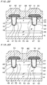
- Fig. 21 is a partial plan view of a U-type IGBT according to another preferred embodiment of the present invention
- Fig. 22 is a partial cross sectional view of some cells of Fig. 21 taken along lines A-A
- Fig. 23 is a partial cross sectional view of some cells of Fig. 21 taken along lines B-B.
- the cells are shown as they are with the emitter electrode 51 and the interlayer insulation film 50 removed.
- Areas C defined by brackets and dashed-and-dotted lines in Fig. 21 are areas which are covered with the interlayer insulation film 50.
- the N + emitter layers 44 which are formed between the groove-shaped inner walls 47 have a ladder-like plan configuration. That is, the N + emitter layers 44 are arranged in the shape of strips, sandwiching the exposed surfaces of the P + semiconductor layers 45.
- the groove-shaped inner walls 47 which include openings at the surfaces of the N + emitter layers 44, extend along the longitudinal extension of the N + emitter layers 44.
- the N + emitter layers 44 which are present between the gate electrodes 49 which are buried in the inner walls are connected to each other through the link portions 55.
- the exposed surfaces of the P + semiconductor layers 45 and the link portions 55 are disposed alternately.
- the areas C of the interlayer insulation film 50 cover the gate electrodes 49 and extend over adjacent N + emitter layers 44 which are adjacent to and along the groove-shaped inner walls 47, and further extend over the exposed surfaces of the P + semiconductor layers 45.
- the emitter electrode 51 contacts the link portions 55 linking the N + emitter layers 44 and the exposed surfaces of the P + semiconductor layers 45, alternately. However, between the link portions 55 which are arranged in a scattered configuration, the N + emitter layers 44 which are sandwiched by the exposed surfaces of the P + semiconductor layers 45 and the groove-shaped inner walls 47 are covered with the interlayer insulation film 50. Hence, these N + emitter layers 44 do not contact the emitter electrode 51.
- the emitter resistance regions 57 are formed within a simple structure in which the interlayer insulation film 50 covers the N + emitter regions 44 which are sandwiched by the exposed surfaces of the P base layer 43 and the groove-shaped inner walls 47, and a breakdown characteristic during short-circuit condition is improved due to the emitter resistances.
- the structure according to the present embodiment is the same as the structure according to the alternative configuration as it is modified to dispose the P + semiconductor layers 45 in the exposed surfaces of the P base layer 43.
- the P + semiconductor layers 45 have an impurity concentration higher than that of the N + emitter regions 44. If the impurity concentration of the N + emitter layers 44 is set at about 1 ⁇ (10 18 - 10 19 ), the impurity concentration of the P + semiconductor layers 45 is set around 2 ⁇ (10 18 - 10 19 ), i.e., about twice higher than the impurity concentration of the N + emitter layers 44.
- the emitter resistance regions 57 are formed within a simple structure in which the diffusion regions of the P + semiconductor layers 45 are expanded, and that the N + emitter layers 44, which are sandwiched between the exposed surfaces of the P + semiconductor layers 45 and the groove-shaped inner walls 47, are covered with the interlayer insulation film 50. Therefore, the breakdown characteristic during shorting is improved without creating a space for disposing emitter resistances and without increasing the cell size.
- the P + semiconductor layers 45 are formed thinner than the N + emitter layers 44 in Fig. 22.
- the contact between the N + emitter layers 44 and the P base layer 43 is made within the link portions 55 of the N + emitter layers 44, not within the N + emitter layers 44 which are sandwiched by the exposed surfaces of the P + layer 45 and the groove-shaped inner walls 47.
- Figs. 24 and 25 are partial cross sectional views of a cell during manufacturing steps in the present embodiment. As compared with the manufacturing processes according to Figs. 6-14 the manufacturing processes according to the present embodiment use a different resist pattern to form the N + emitter regions 65, and also use a different resist pattern to form the interlayer insulation film which is shown in Fig. 13. The other manufacturing steps are similar.
- the resist is stacked on the surface of the P base layer 63, the plurality of the openings which are in the shape of parallel strips and the openings which are linked to these openings are formed by photolithographic processes, the resist pattern in which resists are left scattered in the shape of columns is formed, and using this resist pattern 64 as a mask, N-type impurities are implanted into the surface of the P base layer 63 at a high doping concentration and diffused by annealing to thereby define the N + emitter regions 65.
- the BPSG 72 is stacked on the surface of the polysilicon 69 filling up the grooves formed by the inner walls 67 and on the surface of the thermal oxidation film 68, and the resist 73 is stacked on a surface of the BPSG 72.
- openings surrounding the P + semiconductor layers 71 and the link portions of the N + emitter regions 65 are formed in the resist 73, at areas except for portions of the N + emitter regions 65 which extend along the inner walls 67 and except for portions of the P + semiconductor layers 71 which are in the vicinity of the N + emitter regions 65, to thereby obtain a resist pattern.
- the resist pattern as a mask, the BPSG 72 and the thermal oxidation film 68 are etched, whereby the interlayer insulation film 72 is formed on the surface of the polysilicon 69 which is buried in the grooves which are defined by the inner walls 67 (See Fig. 24). The resist pattern is then removed.
- Al-Si is stacked which serves as a conductive layer, on a surface of the element in which the P + semiconductor layer 71, the N + emitter regions 65 and the interlayer insulation film 72 are disposed. This creates a gate line and a gate pad at the same time which are connected to the polysilicon 69 which is buried in the grooves which are formed by the emitter electrode 73 and the inner walls 67 (See Fig. 25).
- AlMoNiAu alloy which serves as a conductive layer is stacked on the surface of the P + silicon substrate 60, thereby forming a collector electrode 75.
- the U-type IGBT according to the present embodiment is manufactured at an inexpensive cost.
- the present embodiment does not always require to diffuse the P + semiconductor layers 45 shallower than the thickness of the N + emitter layers 44, considering side diffusion, as described earlier.
- P-type impurities may be implanted through the thermal oxidation film 68 at a higher impurity concentration than that of the N + emitter regions 65 and then thermally diffused deeper than the bottom of the N + emitter regions 65 to obtain the P + semiconductor layer 71 whose bottom surface contacts the P base layers 63.
- the present invention is applicable to a U-type IGBT of a P-channel type.
Description
- Fig. 1 is a plan view of an insulated gate semiconductor device according to the present invention. As an example of an insulated gate semiconductor device, a U-type IGBT will be described in the following.
- Fig. 2 is a partial plan view showing some cells of the U-type IGBT of Fig.
1, and Fig. 3 is a partial cross sectional view showing some cells of Fig. 2 taken
along lines A-A. In Fig. 2, the cells are shown as they are with an
emitter electrode 51 and aninterlayer insulation film 50 removed.
Claims (12)
- An insulated gate semiconductor device based on a semiconductor substrate (41, 42, 43, 44, 45) defining an upper major surface and a lower major surface, said insulated gate semiconductor device comprising:whereina first semiconductor layer (41) of a first conductivity type, said first semiconductor layer (41) including a lower surface corresponding to said lower major surface of said semiconductor substrate and an upper surface;a second semiconductor layer (42) of a second conductivity type which is disposed on said upper surface of said first semiconductor layer (41), said second semiconductor layer having a low impurity concentration;a third semiconductor layer (43) of the first conductivity type which is disposed on an upper surface of said second semiconductor layer (42);a plurality of fourth semiconductor layers (44) of the second conductivity type which are disposed parallel to each other in the shape of columns on a portion of an upper surface of said third semiconductor layer (43);a plurality of groove-shaped inner walls (47) defining openings (56) respectively which open in respective upper surfaces of said fourth semiconductor layers (44) so as to extend in a direction along said columns of said fourth semiconductor layers (44), said groove-shaped inner walls (47) extending downward from said surfaces of said fourth semiconductor layers (44) to said second semiconductor layer (42);a fifth semiconductor layer (45) of the first conductivity type which is disposed along said fourth semiconductor layers (44) between adjacent two of said groove-shaped inner walls (47), a junction between said fifth (45) and said fourth (44) semiconductor layers being exposed to said upper major surface;an insulation film (48) covering said groove-shaped inner walls (47);a control electrode (49) which is disposed in the interior of said openings (56) on inner surfaces of said groove-shaped inner walls (47) with said insulation film (48) interposed therebetween;an interlayer insulation film (50) which is disposed on an upper surface of said control electrode (49);a first major electrode (51) which is disposed on said upper surfaces of said fourth (44) and said fifth (45) semiconductor layers and on said interlayer insulation film (50); anda second major electrode (52) which is disposed on said lower second major surface of said first semiconductor substrate layer;
said fifth semiconductor layer has (45) a higher impurity concentration than said fourth semiconductor layers (44) and is disposed on said surfaces of said third (43) and said fourth (44) semiconductor layers to extend across said third (43) and said fourth (44) semiconductor layers;
said insulation film (48) further covers a portion of said upper surfaces of said fourth semiconductor layers (44) which are continuous to, adjacent to, and lying along said groove-shaped inner walls (47);
said control electrode (49) has an upper recessed surface which is recessed from an upper surface of a portion of said insulation film (48) covering a portion of said upper surfaces of said fourth semiconductor layers (44);
in said surface of said third semiconductor layer (43), said fourth semiconductor layers (44) further include a plurality of link portions (55) linking those adjacent portions of said fourth semiconductor layers (44) which are disposed in the shape of columns, in a regularly scattered configuration, so that a surface configuration of said fourth semiconductor layers (44) is a ladder-like configuration in areas which are sandwiched between adjacent two of said groove-shaped inner walls (47); and
exposed upper surfaces of said fifth semiconductor layer (45) are disposed in a regularly scattered configuration along adjacent two of said columns of said fourth semiconductor layers (44) so as to be surrounded by said ladder-like configuration formed by said adjacent portions of said fourth semiconductor layers (44) in the shape of columns and said link portions (55) linking the same. - The insulated gate semiconductor device of claim 1, wherein said insulation film (48) further covers a portion of a surface of said fifth semiconductor layer (45) which is in the vicinity of said columns of said fourth semiconductor layers (44).
- The insulated gate semiconductor device of any of the preceding claims, wherein a bottom surface of said fifth semiconductor layer (45) is located at a position shallower than a bottom surface of said fourth semiconductor layers (44).
- The insulated gate semiconductor device of any of the preceding claims, wherein the impurity concentration of said fifth semiconductor layer (45) is about twice the impurity concentration of said fourth semiconductor layer (44).
- The insulated gate semiconductor device of any of the preceding claims, wherein said upper surface of said conductive material (49) is positioned at a position shallower than the bottom of the fourth semiconductor layers (44).
- The insulated gate semiconductor device of any of the preceding claims, wherein said second semiconductor layer comprises an upper region (42) of an impurity concentration lower than that of a lower region (46) thereof.
- A method of manufacturing an insulated gate semiconductor device according to one of the preceding claims, comprising:a first step of preparing a semiconductor substrate (41, 42; 60, 62) which comprises a first semiconductor layer (41; 60) of a first conductivity type and a second semiconductor layer (42; 62) of a second conductivity type disposed on an upper surface of said first semiconductor layer (41; 60), wherein a lower surface of said first semiconductor layer (60) defines a lower major surface of said semiconductor substrate, and an upper surface of said second semiconductor layer (62) defines an upper major surface of said semiconductor substrate;a second step of implanting impurities of the first conductivity type into said upper major surface of said semiconductor substrate to thereby form a third semiconductor layer (43; 63) of the first conductivity type;a third step of stacking a first resist (64) onto said upper major surface, selectively removing said first resist (64) to leave a portion of said first resist (64) as a plurality of regions which are arranged in the shape of columns parallel to each other and a portion of said first resist (64) as a plurality of regions which are regularly scattered between adjacent two of said parallel column-shaped regions so as to link adjacent two of said column-shaped regions in a ladder-like configuration so that a first resist pattern is formed, selectively implanting impurities of the second conductivity type using said first resist pattern as a mask, and diffusing said impurities of the second conductivity type in an upper surface of said third semiconductor layer (63) to thereby form fourth semiconductor layers (44; 65) of the second conductivity type having a higher impurity concentration than said upper region of said second semiconductor layer (62);a fourth step of forming a shielding film (66) on said upper major surface, forming an opening in said shielding film (66) on a portion of an upper surface of said fourth (65) semiconductor layers so that said opening extends along an upper surface of said columns of said fourth semiconductor layers (65), selectively removing a semiconductor down to said second semiconductor layer (62) while using said shielding film (66) as a mask which includes said opening to thereby form groove-shaped inner walls (67) which define grooves, and thereafter removing said shielding film (66);a fifth step of forming an insulation film (68) on surfaces of said groove-shaped inner walls (67) and on said upper major surface;a sixth step of stacking a conductive material (69) on said insulation film (68) so that said grooves are filled up;a seventh step of uniformly removing said conductive material (69) while leaving said insulation film (68) until an upper surface of said conductive material (69) which is buried in said grooves is recessed from a surface of a portion of said insulation film (68) which is formed on said upper major surface;an eighth step of stacking a second resist (70) on a portion of said insulation film (69), which is exposed on said upper major surface after said seventh step, and said surface of said conductive material (69), forming an opening therein at such a position as to surround an area which corresponds to said first resist (64) which is left at said third step in the shape of said ladder-like configuration of column-shaped regions and scattered portions and to surround portions of surfaces of said fourth semiconductor layers (65) which are adjacent to said area of said opening in said second resist (70), and to surround portions of surfaces of said fourth semiconductor layers (65) which are adjacent to said area, selectively implanting impurities of the first conductivity type at a higher impurity concentration than that of said fourth semiconductor layers (65) through said insulation film (68) while using said second resist (70) as a mask which includes said opening, and diffusing said impurities of the first conductivity type to thereby selectively form a fifth semiconductor layer (71) of the first conductivity type connecting said third semiconductor layer (63);a ninth step of stacking an insulation material (72) on said portion of said insulation film (68), which is exposed after said seventh step, and on said upper surface of said conductive material (69);a tenth step of stacking a third resist (73) on an upper surface of said insulation material (72), forming an opening therein which surrounds said fifth semiconductor layer (71) and portions of said fourth semiconductor layers (65), except for said portions of said upper surfaces of said fourth semiconductor layers (65) which are adjacent to and along said inner walls (67), selectively removing said insulation material (72) and said insulation film (68) while using said third resist (73) as a mask which includes said opening to thereby expose said fifth semiconductor layer (71) and said fourth semiconductor layers (65);an eleventh step of stacking a conductive layer (74) on said fourth (65) and fifth (71) semiconductor layers which are exposed after said tenth step and on said surface of said insulation material (72); anda twelfth step of stacking a conductive layer (75) on said lower major surface of said semiconductor substrate.
- The method of claim 7, wherein at said tenth step said opening is formed in said third resist (73) stacked on said insulation material (72) as to surround said fifth semiconductor layer (71) and portions of said fourth semiconductor layers (65), further except for a portion of an upper surface of said fifth semiconductor layer (71).
- The method of any of claims 7-8, wherein at said eight step said impurities of the first conductivity type are diffused shallower than the bottom of said fourth semiconductor layers (65) whose bottom surface contacts said third semiconductor layer (63).
- The method of any of claims 7-9, wherein at said eight step said impurities of the first conductivity type are diffused at an impurity concentration of about twice the impurity concentration of said fourth semiconductor layers (65).
- The method of any of claims 7-10, wherein at said seventh step the removing of said conductive material (69) is performed so that said upper surface of said conductive material (69) is positioned at a position shallower than the bottom of the fourth semiconductor layers (65).
- The method of any of claims 7-11, said second semiconductor layer comprising an upper region (62) of an impurity concentration lower than that of a lower region (61) thereof.
Priority Applications (2)
| Application Number | Priority Date | Filing Date | Title |
|---|---|---|---|
| EP02012507A EP1237201B1 (en) | 1995-07-21 | 1996-05-09 | Insulated gate semiconductor device |
| EP02008520A EP1233457B1 (en) | 1995-07-21 | 1996-05-09 | Insulated gate semiconductor device and method of manufacturing the same |
Applications Claiming Priority (3)
| Application Number | Priority Date | Filing Date | Title |
|---|---|---|---|
| JP185783/95 | 1995-07-21 | ||
| JP18578395A JP3384198B2 (en) | 1995-07-21 | 1995-07-21 | Insulated gate semiconductor device and method of manufacturing the same |
| JP18578395 | 1995-07-21 |
Related Child Applications (4)
| Application Number | Title | Priority Date | Filing Date |
|---|---|---|---|
| EP02012507A Division EP1237201B1 (en) | 1995-07-21 | 1996-05-09 | Insulated gate semiconductor device |
| EP02008520A Division EP1233457B1 (en) | 1995-07-21 | 1996-05-09 | Insulated gate semiconductor device and method of manufacturing the same |
| EP02008520.5 Division-Into | 2002-04-15 | ||
| EP02012507.6 Division-Into | 2002-06-04 |
Publications (3)
| Publication Number | Publication Date |
|---|---|
| EP0755076A2 EP0755076A2 (en) | 1997-01-22 |
| EP0755076A3 EP0755076A3 (en) | 1997-02-19 |
| EP0755076B1 true EP0755076B1 (en) | 2003-07-30 |
Family
ID=16176826
Family Applications (3)
| Application Number | Title | Priority Date | Filing Date |
|---|---|---|---|
| EP96107393A Expired - Lifetime EP0755076B1 (en) | 1995-07-21 | 1996-05-09 | Vertical MOS semiconductor with recessed gate and method of manufacturing the same |
| EP02012507A Expired - Lifetime EP1237201B1 (en) | 1995-07-21 | 1996-05-09 | Insulated gate semiconductor device |
| EP02008520A Expired - Lifetime EP1233457B1 (en) | 1995-07-21 | 1996-05-09 | Insulated gate semiconductor device and method of manufacturing the same |
Family Applications After (2)
| Application Number | Title | Priority Date | Filing Date |
|---|---|---|---|
| EP02012507A Expired - Lifetime EP1237201B1 (en) | 1995-07-21 | 1996-05-09 | Insulated gate semiconductor device |
| EP02008520A Expired - Lifetime EP1233457B1 (en) | 1995-07-21 | 1996-05-09 | Insulated gate semiconductor device and method of manufacturing the same |
Country Status (5)
| Country | Link |
|---|---|
| US (2) | US5801408A (en) |
| EP (3) | EP0755076B1 (en) |
| JP (1) | JP3384198B2 (en) |
| KR (2) | KR100250350B1 (en) |
| DE (3) | DE69629251T2 (en) |
Cited By (1)
| Publication number | Priority date | Publication date | Assignee | Title |
|---|---|---|---|---|
| US7736978B2 (en) | 1997-11-14 | 2010-06-15 | Fairchild Semiconductor Corporation | Method of manufacturing a trench transistor having a heavy body region |
Families Citing this family (64)
| Publication number | Priority date | Publication date | Assignee | Title |
|---|---|---|---|---|
| US6204533B1 (en) * | 1995-06-02 | 2001-03-20 | Siliconix Incorporated | Vertical trench-gated power MOSFET having stripe geometry and high cell density |
| JP3410286B2 (en) | 1996-04-01 | 2003-05-26 | 三菱電機株式会社 | Insulated gate semiconductor device |
| DE19727676A1 (en) * | 1997-06-30 | 1999-01-07 | Asea Brown Boveri | MOS controlled power semiconductor component |
| JP3281844B2 (en) * | 1997-08-26 | 2002-05-13 | 三洋電機株式会社 | Method for manufacturing semiconductor device |
| JP3164030B2 (en) * | 1997-09-19 | 2001-05-08 | 日本電気株式会社 | Manufacturing method of vertical field effect transistor |
| JP3281847B2 (en) * | 1997-09-26 | 2002-05-13 | 三洋電機株式会社 | Method for manufacturing semiconductor device |
| SE9800286D0 (en) * | 1998-02-02 | 1998-02-02 | Abb Research Ltd | A transistor of SiC |
| DE19808154A1 (en) * | 1998-02-27 | 1999-09-02 | Asea Brown Boveri | Bipolar transistor with insulated gate (IGBT) |
| EP1060517A1 (en) | 1998-02-27 | 2000-12-20 | ABB Semiconductors AG | Bipolar transistor with an insulated gate electrode |
| EP1081769A4 (en) | 1998-04-27 | 2007-05-02 | Mitsubishi Electric Corp | Semiconductor device and process for manufacturing the same |
| KR100451450B1 (en) | 1998-12-18 | 2004-10-06 | 인피니언 테크놀로지스 아게 | Field effect transistor arrangement with a trench gate electrode and an additional highly doped layer in the body region |
| GB2347014B (en) * | 1999-02-18 | 2003-04-16 | Zetex Plc | Semiconductor device |
| US6351009B1 (en) * | 1999-03-01 | 2002-02-26 | Fairchild Semiconductor Corporation | MOS-gated device having a buried gate and process for forming same |
| US6413822B2 (en) | 1999-04-22 | 2002-07-02 | Advanced Analogic Technologies, Inc. | Super-self-aligned fabrication process of trench-gate DMOS with overlying device layer |
| JP2001085685A (en) * | 1999-09-13 | 2001-03-30 | Shindengen Electric Mfg Co Ltd | Transistor |
| JP2001102575A (en) * | 1999-09-29 | 2001-04-13 | Nec Corp | Semiconductor device and temperature detection method therefor |
| US6392273B1 (en) * | 2000-01-14 | 2002-05-21 | Rockwell Science Center, Llc | Trench insulated-gate bipolar transistor with improved safe-operating-area |
| DE10009345C1 (en) * | 2000-02-28 | 2001-07-19 | Infineon Technologies Ag | Field effect transistor device with trench-shaped gate electrode |
| DE10023950A1 (en) * | 2000-05-16 | 2001-11-22 | Bosch Gmbh Robert | Semiconductor component with power switch connectable to load |
| JP2002110978A (en) * | 2000-10-02 | 2002-04-12 | Toshiba Corp | Power semiconductor element |
| US6593620B1 (en) * | 2000-10-06 | 2003-07-15 | General Semiconductor, Inc. | Trench DMOS transistor with embedded trench schottky rectifier |
| JP3708014B2 (en) * | 2000-10-20 | 2005-10-19 | 株式会社東芝 | Semiconductor device |
| JP4088033B2 (en) * | 2000-11-27 | 2008-05-21 | 株式会社東芝 | Semiconductor device |
| EP1271654B1 (en) * | 2001-02-01 | 2017-09-20 | Mitsubishi Denki Kabushiki Kaisha | Semiconductor device and method of manufacturing the same |
| DE60139386D1 (en) * | 2001-02-02 | 2009-09-10 | Mitsubishi Electric Corp | SEMICONDUCTOR ARRANGEMENT WITH A BIPOLAR TRANSISTOR WITH INSULATED GATE AND FREE CIRCUIT DIODE |
| JP4823435B2 (en) * | 2001-05-29 | 2011-11-24 | 三菱電機株式会社 | Semiconductor device and manufacturing method thereof |
| GB0208833D0 (en) * | 2002-04-18 | 2002-05-29 | Koninkl Philips Electronics Nv | Trench-gate semiconductor devices |
| EP1597769B1 (en) * | 2003-02-18 | 2010-09-29 | Nxp B.V. | Semiconductor device and method of manufacturing such a device |
| JP2005057235A (en) * | 2003-07-24 | 2005-03-03 | Mitsubishi Electric Corp | Insulated gate type bipolar transistor, its manufacturing method, and inverter circuit |
| JP4799829B2 (en) * | 2003-08-27 | 2011-10-26 | 三菱電機株式会社 | Insulated gate transistor and inverter circuit |
| US7259411B1 (en) * | 2003-12-04 | 2007-08-21 | National Semiconductor Corporation | Vertical MOS transistor |
| JP4059846B2 (en) | 2003-12-26 | 2008-03-12 | Necエレクトロニクス株式会社 | Semiconductor device and manufacturing method thereof |
| JP2006012967A (en) * | 2004-06-23 | 2006-01-12 | Toshiba Corp | Semiconductor device |
| JP2006120789A (en) * | 2004-10-20 | 2006-05-11 | Toshiba Corp | Semiconductor device |
| JP4212552B2 (en) * | 2004-12-22 | 2009-01-21 | 株式会社東芝 | Semiconductor device |
| JP4440188B2 (en) * | 2005-01-19 | 2010-03-24 | パナソニック株式会社 | Manufacturing method of semiconductor device |
| JP2006228906A (en) * | 2005-02-16 | 2006-08-31 | Sanyo Electric Co Ltd | Semiconductor device and its manufacturing method |
| JP4928753B2 (en) * | 2005-07-14 | 2012-05-09 | 株式会社東芝 | Trench gate type semiconductor device |
| JP4939012B2 (en) | 2005-08-26 | 2012-05-23 | ルネサスエレクトロニクス株式会社 | Semiconductor device |
| JP2007081107A (en) * | 2005-09-14 | 2007-03-29 | Elpida Memory Inc | Semiconductor device and manufacturing method thereof |
| JP5984282B2 (en) * | 2006-04-27 | 2016-09-06 | 富士電機株式会社 | Vertical trench insulated gate MOS semiconductor device |
| JP5040240B2 (en) * | 2006-09-29 | 2012-10-03 | 三菱電機株式会社 | Insulated gate semiconductor device |
| JP5383009B2 (en) * | 2007-07-17 | 2014-01-08 | 三菱電機株式会社 | Semiconductor device design method |
| JP5767430B2 (en) * | 2007-08-10 | 2015-08-19 | ローム株式会社 | Semiconductor device and manufacturing method of semiconductor device |
| JP2009164183A (en) * | 2007-12-28 | 2009-07-23 | Toshiba Corp | Semiconductor device, and manufacturing method thereof |
| US8022470B2 (en) * | 2008-09-04 | 2011-09-20 | Infineon Technologies Austria Ag | Semiconductor device with a trench gate structure and method for the production thereof |
| JP5423018B2 (en) * | 2009-02-02 | 2014-02-19 | 三菱電機株式会社 | Semiconductor device |
| JP5687582B2 (en) * | 2010-09-21 | 2015-03-18 | 株式会社東芝 | Semiconductor device and manufacturing method thereof |
| TWI462294B (en) * | 2010-09-21 | 2014-11-21 | Toshiba Kk | Semiconductor element and manufacturing method thereof |
| US8384151B2 (en) * | 2011-01-17 | 2013-02-26 | Infineon Technologies Austria Ag | Semiconductor device and a reverse conducting IGBT |
| JP5700649B2 (en) * | 2011-01-24 | 2015-04-15 | 旭化成エレクトロニクス株式会社 | Manufacturing method of semiconductor device |
| CN102891082B (en) * | 2011-07-18 | 2015-09-23 | 中国科学院微电子研究所 | Igbt and preparation method thereof |
| US8766325B2 (en) | 2011-10-17 | 2014-07-01 | Rohm Co., Ltd. | Semiconductor device |
| JP5754397B2 (en) * | 2012-03-09 | 2015-07-29 | 三菱電機株式会社 | Manufacturing method of vertical trench IGBT |
| KR20150076815A (en) * | 2013-12-27 | 2015-07-07 | 삼성전기주식회사 | Power semiconductor device |
| JP6237408B2 (en) * | 2014-03-28 | 2017-11-29 | 住友電気工業株式会社 | Silicon carbide semiconductor device and manufacturing method thereof |
| US10608104B2 (en) | 2014-03-28 | 2020-03-31 | Infineon Technologies Ag | Trench transistor device |
| US20160013301A1 (en) * | 2014-07-10 | 2016-01-14 | Nuvoton Technology Corporation | Semiconductor device and method of manufacturing the same |
| JP6507112B2 (en) * | 2016-03-16 | 2019-04-24 | 株式会社東芝 | Semiconductor device |
| CN108321188B (en) * | 2017-01-18 | 2021-02-09 | 中芯国际集成电路制造(上海)有限公司 | Insulated gate bipolar transistor and forming method thereof |
| JP6817116B2 (en) * | 2017-03-14 | 2021-01-20 | エイブリック株式会社 | Semiconductor device |
| JP2018207057A (en) * | 2017-06-09 | 2018-12-27 | ルネサスエレクトロニクス株式会社 | Semiconductor device and method for manufacturing the same |
| CN107516669B (en) * | 2017-08-07 | 2021-02-12 | 电子科技大学 | IGBT device |
| JP7263715B2 (en) | 2018-08-30 | 2023-04-25 | 富士電機株式会社 | Semiconductor device manufacturing method and semiconductor device |
Citations (1)
| Publication number | Priority date | Publication date | Assignee | Title |
|---|---|---|---|---|
| EP0485059A2 (en) * | 1990-09-28 | 1992-05-13 | Kabushiki Kaisha Toshiba | Semiconductor device including a pin-diode having high breakdown voltage |
Family Cites Families (20)
| Publication number | Priority date | Publication date | Assignee | Title |
|---|---|---|---|---|
| FR2507820A1 (en) * | 1981-06-16 | 1982-12-17 | Thomson Csf | BIPOLAR FIELD EFFECT CONTROL TRANSISTOR USING ISLE GRID |
| EP0159663A3 (en) * | 1984-04-26 | 1987-09-23 | General Electric Company | High-density v-groove mos-controlled thyristors, insulated-gate transistors, and mosfets, and methods for fabrication |
| JPS60235275A (en) * | 1984-05-08 | 1985-11-21 | Kontetsuku:Kk | Computer supporting measuring system |
| US4860072A (en) * | 1986-03-05 | 1989-08-22 | Ixys Corporation | Monolithic semiconductor device and method of manufacturing same |
| US5034785A (en) * | 1986-03-24 | 1991-07-23 | Siliconix Incorporated | Planar vertical channel DMOS structure |
| JPH07123165B2 (en) * | 1986-08-19 | 1995-12-25 | 松下電子工業株式会社 | Vertical MOS field effect transistor |
| JPH01198076A (en) * | 1988-02-02 | 1989-08-09 | Mitsubishi Electric Corp | Semiconductor device |
| JPH0734474B2 (en) * | 1988-03-03 | 1995-04-12 | 富士電機株式会社 | Method for manufacturing conductivity modulation type MOSFET |
| JP2858404B2 (en) * | 1990-06-08 | 1999-02-17 | 株式会社デンソー | Insulated gate bipolar transistor and method of manufacturing the same |
| JP2504862B2 (en) * | 1990-10-08 | 1996-06-05 | 三菱電機株式会社 | Semiconductor device and manufacturing method thereof |
| US5182222A (en) * | 1991-06-26 | 1993-01-26 | Texas Instruments Incorporated | Process for manufacturing a DMOS transistor |
| EP0550770B1 (en) * | 1991-07-26 | 1997-11-12 | Denso Corporation | Method of producing vertical mosfets |
| GB9215653D0 (en) * | 1992-07-23 | 1992-09-09 | Philips Electronics Uk Ltd | A method of manufacturing a semiconductor device comprising an insulated gate field effect device |
| GB9216599D0 (en) * | 1992-08-05 | 1992-09-16 | Philips Electronics Uk Ltd | A semiconductor device comprising a vertical insulated gate field effect device and a method of manufacturing such a device |
| US5326711A (en) * | 1993-01-04 | 1994-07-05 | Texas Instruments Incorporated | High performance high voltage vertical transistor and method of fabrication |
| JP3204792B2 (en) * | 1993-04-27 | 2001-09-04 | 株式会社東芝 | Semiconductor device |
| GB9313843D0 (en) * | 1993-07-05 | 1993-08-18 | Philips Electronics Uk Ltd | A semiconductor device comprising an insulated gate field effect transistor |
| US5405794A (en) * | 1994-06-14 | 1995-04-11 | Philips Electronics North America Corporation | Method of producing VDMOS device of increased power density |
| JPH08306914A (en) * | 1995-04-27 | 1996-11-22 | Nippondenso Co Ltd | Semiconductor device and its manufacture |
| US5567634A (en) * | 1995-05-01 | 1996-10-22 | National Semiconductor Corporation | Method of fabricating self-aligned contact trench DMOS transistors |
-
1995
- 1995-07-21 JP JP18578395A patent/JP3384198B2/en not_active Expired - Lifetime
-
1996
- 1996-02-13 US US08/601,161 patent/US5801408A/en not_active Expired - Lifetime
- 1996-05-09 DE DE69629251T patent/DE69629251T2/en not_active Expired - Lifetime
- 1996-05-09 EP EP96107393A patent/EP0755076B1/en not_active Expired - Lifetime
- 1996-05-09 DE DE69636913T patent/DE69636913T2/en not_active Expired - Lifetime
- 1996-05-09 EP EP02012507A patent/EP1237201B1/en not_active Expired - Lifetime
- 1996-05-09 EP EP02008520A patent/EP1233457B1/en not_active Expired - Lifetime
- 1996-05-09 DE DE69637366T patent/DE69637366T2/en not_active Expired - Lifetime
- 1996-06-07 KR KR1019960020385A patent/KR100250350B1/en not_active IP Right Cessation
-
1997
- 1997-09-29 US US08/939,496 patent/US5960264A/en not_active Expired - Lifetime
-
1999
- 1999-10-20 KR KR1019990045552A patent/KR100292720B1/en not_active IP Right Cessation
Patent Citations (1)
| Publication number | Priority date | Publication date | Assignee | Title |
|---|---|---|---|---|
| EP0485059A2 (en) * | 1990-09-28 | 1992-05-13 | Kabushiki Kaisha Toshiba | Semiconductor device including a pin-diode having high breakdown voltage |
Cited By (1)
| Publication number | Priority date | Publication date | Assignee | Title |
|---|---|---|---|---|
| US7736978B2 (en) | 1997-11-14 | 2010-06-15 | Fairchild Semiconductor Corporation | Method of manufacturing a trench transistor having a heavy body region |
Also Published As
| Publication number | Publication date |
|---|---|
| EP1237201B1 (en) | 2007-12-12 |
| JP3384198B2 (en) | 2003-03-10 |
| DE69636913D1 (en) | 2007-03-29 |
| EP0755076A3 (en) | 1997-02-19 |
| EP1233457B1 (en) | 2007-02-14 |
| EP1233457A2 (en) | 2002-08-21 |
| DE69629251T2 (en) | 2004-04-22 |
| EP1237201A2 (en) | 2002-09-04 |
| DE69629251D1 (en) | 2003-09-04 |
| KR100292720B1 (en) | 2001-06-15 |
| US5960264A (en) | 1999-09-28 |
| DE69637366T2 (en) | 2008-12-04 |
| JPH0936362A (en) | 1997-02-07 |
| KR970008651A (en) | 1997-02-24 |
| EP0755076A2 (en) | 1997-01-22 |
| EP1233457A3 (en) | 2003-04-23 |
| EP1237201A3 (en) | 2003-04-23 |
| KR100250350B1 (en) | 2000-04-01 |
| DE69637366D1 (en) | 2008-01-24 |
| US5801408A (en) | 1998-09-01 |
| DE69636913T2 (en) | 2007-11-15 |
Similar Documents
| Publication | Publication Date | Title |
|---|---|---|
| EP0755076B1 (en) | Vertical MOS semiconductor with recessed gate and method of manufacturing the same | |
| JP3288218B2 (en) | Insulated gate semiconductor device and method of manufacturing the same | |
| EP0801425B1 (en) | Insulated gate semiconductor device and method of manufacturing the same | |
| EP0732749B1 (en) | Insulated gate bipolar semiconductor device and manufacturing method thereof | |
| KR100218873B1 (en) | Insulated gate semiconductor device and manufacturing method thereof | |
| EP1154491B1 (en) | Semiconductor with pnpn structure | |
| EP1895595B1 (en) | Semiconductor device and electric power conversion apparatus therewith | |
| EP1094525B1 (en) | Field-effect semiconductor device having a trench gate electrode and method of making the same | |
| EP0760529B1 (en) | Lateral IGBT | |
| US6001678A (en) | Insulated gate semiconductor device | |
| US6768168B1 (en) | Insulated gate semiconductor device with low on voltage and manufacturing method thereof | |
| US6747295B2 (en) | Semiconductor device with trench gate | |
| US5451531A (en) | Method of fabricating an insulated gate semiconductor device | |
| JP3120389B2 (en) | Semiconductor device | |
| JPH0846193A (en) | Semiconductor device | |
| US5869850A (en) | Lateral insulated gate bipolar transistor | |
| EP0658939B1 (en) | Voltage-driven thyristor and method of manufacturing the same | |
| KR100269631B1 (en) | Insulated gate bipolar transistor and manufacturing method thereof |
Legal Events
| Date | Code | Title | Description |
|---|---|---|---|
| PUAI | Public reference made under article 153(3) epc to a published international application that has entered the european phase |
Free format text: ORIGINAL CODE: 0009012 |
|
| PUAL | Search report despatched |
Free format text: ORIGINAL CODE: 0009013 |
|
| AK | Designated contracting states |
Kind code of ref document: A2 Designated state(s): DE FR GB |
|
| AK | Designated contracting states |
Kind code of ref document: A3 Designated state(s): DE FR GB |
|
| 17P | Request for examination filed |
Effective date: 19970318 |
|
| 17Q | First examination report despatched |
Effective date: 19990427 |
|
| GRAG | Despatch of communication of intention to grant |
Free format text: ORIGINAL CODE: EPIDOS AGRA |
|
| GRAG | Despatch of communication of intention to grant |
Free format text: ORIGINAL CODE: EPIDOS AGRA |
|
| GRAH | Despatch of communication of intention to grant a patent |
Free format text: ORIGINAL CODE: EPIDOS IGRA |
|
| GRAH | Despatch of communication of intention to grant a patent |
Free format text: ORIGINAL CODE: EPIDOS IGRA |
|
| GRAA | (expected) grant |
Free format text: ORIGINAL CODE: 0009210 |
|
| AK | Designated contracting states |
Designated state(s): DE FR GB |
|
| REG | Reference to a national code |
Ref country code: GB Ref legal event code: FG4D |
|
| REF | Corresponds to: |
Ref document number: 69629251 Country of ref document: DE Date of ref document: 20030904 Kind code of ref document: P |
|
| ET | Fr: translation filed | ||
| PLBE | No opposition filed within time limit |
Free format text: ORIGINAL CODE: 0009261 |
|
| STAA | Information on the status of an ep patent application or granted ep patent |
Free format text: STATUS: NO OPPOSITION FILED WITHIN TIME LIMIT |
|
| 26N | No opposition filed |
Effective date: 20040504 |
|
| REG | Reference to a national code |
Ref country code: FR Ref legal event code: ST Effective date: 20090119 |
|
| PG25 | Lapsed in a contracting state [announced via postgrant information from national office to epo] |
Ref country code: FR Free format text: LAPSE BECAUSE OF NON-PAYMENT OF DUE FEES Effective date: 20080602 |
|
| REG | Reference to a national code |
Ref country code: GB Ref legal event code: 746 Effective date: 20100615 |
|
| REG | Reference to a national code |
Ref country code: FR Ref legal event code: D3 Effective date: 20111018 |
|
| PGRI | Patent reinstated in contracting state [announced from national office to epo] |
Ref country code: FR Effective date: 20111018 |
|
| REG | Reference to a national code |
Ref country code: FR Ref legal event code: PLFP Year of fee payment: 20 |
|
| PGFP | Annual fee paid to national office [announced via postgrant information from national office to epo] |
Ref country code: GB Payment date: 20150506 Year of fee payment: 20 Ref country code: DE Payment date: 20150506 Year of fee payment: 20 |
|
| PGFP | Annual fee paid to national office [announced via postgrant information from national office to epo] |
Ref country code: FR Payment date: 20150508 Year of fee payment: 20 |
|
| REG | Reference to a national code |
Ref country code: DE Ref legal event code: R071 Ref document number: 69629251 Country of ref document: DE |
|
| REG | Reference to a national code |
Ref country code: GB Ref legal event code: PE20 Expiry date: 20160508 |
|
| PG25 | Lapsed in a contracting state [announced via postgrant information from national office to epo] |
Ref country code: GB Free format text: LAPSE BECAUSE OF EXPIRATION OF PROTECTION Effective date: 20160508 |