EP0752733B1 - Wellenleiter-Resonatoranordnung sowie Verwendung - Google Patents
Wellenleiter-Resonatoranordnung sowie Verwendung Download PDFInfo
- Publication number
- EP0752733B1 EP0752733B1 EP96110858A EP96110858A EP0752733B1 EP 0752733 B1 EP0752733 B1 EP 0752733B1 EP 96110858 A EP96110858 A EP 96110858A EP 96110858 A EP96110858 A EP 96110858A EP 0752733 B1 EP0752733 B1 EP 0752733B1
- Authority
- EP
- European Patent Office
- Prior art keywords
- waveguide
- dielectric insert
- resonator assembly
- assembly according
- plate
- Prior art date
- Legal status (The legal status is an assumption and is not a legal conclusion. Google has not performed a legal analysis and makes no representation as to the accuracy of the status listed.)
- Expired - Lifetime
Links
- 239000004020 conductor Substances 0.000 claims description 4
- 239000000463 material Substances 0.000 claims description 4
- 239000010453 quartz Substances 0.000 claims description 4
- VYPSYNLAJGMNEJ-UHFFFAOYSA-N silicon dioxide Inorganic materials O=[Si]=O VYPSYNLAJGMNEJ-UHFFFAOYSA-N 0.000 claims description 4
- 239000000919 ceramic Substances 0.000 claims description 3
- 239000010432 diamond Substances 0.000 claims description 3
- 229910003460 diamond Inorganic materials 0.000 claims description 3
- 229910052594 sapphire Inorganic materials 0.000 claims description 3
- 239000010980 sapphire Substances 0.000 claims description 3
- 239000002887 superconductor Substances 0.000 claims description 2
- 230000000712 assembly Effects 0.000 claims 1
- 238000000429 assembly Methods 0.000 claims 1
- 230000008646 thermal stress Effects 0.000 description 4
- 230000017525 heat dissipation Effects 0.000 description 3
- 229910000859 α-Fe Inorganic materials 0.000 description 2
- 230000001133 acceleration Effects 0.000 description 1
- 230000009471 action Effects 0.000 description 1
- 230000008859 change Effects 0.000 description 1
- 230000008878 coupling Effects 0.000 description 1
- 238000010168 coupling process Methods 0.000 description 1
- 238000005859 coupling reaction Methods 0.000 description 1
- 239000003292 glue Substances 0.000 description 1
- 238000001465 metallisation Methods 0.000 description 1
- 230000004048 modification Effects 0.000 description 1
- 238000012986 modification Methods 0.000 description 1
- 230000035882 stress Effects 0.000 description 1
Images


Classifications
-
- H—ELECTRICITY
- H01—ELECTRIC ELEMENTS
- H01P—WAVEGUIDES; RESONATORS, LINES, OR OTHER DEVICES OF THE WAVEGUIDE TYPE
- H01P1/00—Auxiliary devices
- H01P1/20—Frequency-selective devices, e.g. filters
- H01P1/207—Hollow waveguide filters
- H01P1/208—Cascaded cavities; Cascaded resonators inside a hollow waveguide structure
- H01P1/2084—Cascaded cavities; Cascaded resonators inside a hollow waveguide structure with dielectric resonators
Definitions
- the invention is based on a waveguide resonator arrangement according to the preamble of the main claim.
- EP 438 807 B1 discloses a waveguide resonator arrangement known with a plurality of support rods having a dielectric Fix the insert centered in the waveguide.
- the support rods are on Waveguides attached and submerged in the dielectric insert corresponding holes on its outer circumference.
- EP 351 840 A2 likewise discloses a resonator with dielectric insert.
- the insert is held by two plates, have the special centering devices. By grasping the use of the centering can thermal Tensions arise.
- EP 328 948 B1 also discloses a dielectric waveguide resonator, wherein the dielectric insert can be centrally fixed in the waveguide in a feed system that can be adjusted using three screws.
- US Pat. No. 3,155,965 discloses a support structure for a ferrite body in a waveguide with radial support pins mounted on the outer circumference of the ferrite body.
- the waveguide resonator arrangement with the features of Claim 1 is suitable, thermal stresses better to be collected as the arrangements mentioned above, because the pressure exerted on the dielectric insert is adjustable and there are none special versions are available.
- the arrangement of Invention is easy to produce. So z. Eg none Holes may be provided in the dielectric insert such as in the subject matter of EP 438 807 B1. An elaborate Feeding system as in EP 328 948 B1 is not necessary. Nevertheless, a very accurate fixation / holder of the dielectric insert in the Wave propagation direction of waveguide (waveguide) through the support device and perpendicular thereto, ie in a cross-sectional plane of the waveguide possible without thermal stresses are unfavorable.
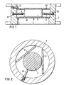
- FIG. 1 shows a waveguide resonator arrangement with one example, as a circular waveguide resonator formed waveguide 1 with a dielectric Insert 2, which is preferably arranged centrally in the waveguide is.
- the dielectric insert 2 consists in that in FIG. 1 shown embodiment of a disc-shaped Cylinder. In one embodiment, not shown the dielectric insert may be spherical.
- the Dielectric insert 2 consists for example of a dielectric ceramic with a high Dielectric constant of, for example, 10 to 50th
- Dielectric insert 2 consists for example of a dielectric ceramic with a high Dielectric constant of, for example, 10 to 50th
- clamping body 3 Between an outer periphery of the dielectric insert - here between cylinder jacket and waveguide 1 - are several Clamping body 3 is provided, which radially to the clamping body. 3 run in and only touch it tangentially.
- the clamping bodies 3 are made Quartz rods, which are preferably uniform in one plane are distributed and by threaded screws 31 in the waveguide first delivered towards the dielectric insert 3 out can be to the desired clamping pressure as well as the desired position (here center position of the dielectric Use in the waveguide 1) set.
- the desired clamping pressure as well as the desired position (here center position of the dielectric Use in the waveguide 1) set.
- the desired position here center position of the dielectric Use in the waveguide 1 set.
- a Support device 4 is provided for fixing the dielectric insert 2 in one Direction (here z-direction), by the / the Fixation direction / s (here x, y direction in a Transverse plane of the waveguide) of the dielectric insert 2 deviates by the clamp body 3 .
- This support device consists in the embodiment shown of two plates 41st and 42, wherein a plate 41 on a shoulder 5 in Waveguide 1 rests, the diameter jump in Waveguide represents.
- Another plate 42 is located on the opposite top surface of the cylindrical dielectric insert 2.
- the latter plate 42 is a Assigned clamping device 6, z. B. in the form of a Madenklemmschraube, by means of which the plate 42 in the direction the plate 41 is deliverable.
- the support device 4 is thus the dielectric insert in the z-direction fixable.
- the upper plate 42 may be omitted.
- the plate (s) 41 and 42 respectively preferably also made of quartz for thermal reasons.
- the plates 41 and 42 preferably have no Centering devices, such as steps, webs, etc., the to could lead to unfavorable thermal stresses.
- FIG. 2 shows a cross section through the circular waveguide 1 with a modification for the clamp body 3.
- Two of the Clamping body 31 and 32 consist of vertically in the waveguide first standing plates preferably made of quartz or ceramic, the Touch the dielectric insert 2 tangentially.
- the third Clamping body 33 consists as before of a rod, which means a screw on the dielectric insert deliverable is and to set the necessary clamping pressure suitable is.
- Figure 3 shows a to this Embodiment associated longitudinal section.
- the clamping body 3 consist of circular cylinders or balls, by means of grub screws radially toward dielectric Insert 2 are deliverable. Also in this Embodiment touching the clamp body 3 the Circular cylinder - or spherical designed dielectric insert 2 - only tangential.
- the Support device 4 from at least one other There are clamping body, which is suitable, a clamping action on the dielectric insert 2 in an axial direction to be determined by the orientation (s) used to fix the dielectric insert 2 by the clamping body 3 differs.
- the dielectric insert 2 is here is also cylindrical, mechanically rigid relative to the support device - plate 41 - fixed.
- the Plate 41 is at its outer periphery in a holder 8, which is attached to the inner edge of the waveguide 1, stored.
- the fixation of the insert 2 on the plate 41st is areal, for example, via a suitable Glue 7 with good thermal conductivity.
- the plate 41 consists of an electrically poorly conductive material which preferably good heat-conducting. As materials for this suitable are diamond or sapphire.
- Both by the planar fixation as well as by the good thermal conductivity Plate 41 can be a good heat transfer from the dielectric Insert 2 to the waveguide outer wall / Resonatorwand done and thus the loss energy generated in the dielectric be dissipated quickly.
- the paragraph 5 be used in the waveguide 1 against which the plate 41st is pressed by means of a clamping device.
- Clamping device are not suitable, for example metallic screws 61, 62 made of plastic, which in one Angle of about 45 ° are guided in the waveguide wall 1 and Press the plate 41 against the heel 5.
- the Support device 4 from a further plate 42, the in particular adhered to the dielectric insert.
- the Plate 42 may be with a similar holder as before be provided.
- additional clamping body 3 in Shape of pins, cylinders, etc. from good heat-conducting but electrical poorly conductive material such as diamond or Sapphire tangential to the outer shell of the insert 2 can touch, can be provided for further heat dissipation.
- these clamp body with the use of 2 glued thermally conductive.
- the Plate 41 and / or the plate 42 at its outer edge with be solderable material coated such that the plate 41 and 42 to the paragraph 5 and / or to the waveguide inner wall is solderable.
- the dielectric insert 2 soldered to the plate 41 and 42, respectively if a corresponding metallization takes place beforehand is.
- At least one of the clamping body 3, the support device 4, the waveguide inner wall, the dielectric insert 2 and / or the further clamping body can be connected to a superconductor completely or partially coated. In this way it is possible to reduce losses and the resonator quality increase.
- the waveguide resonator arrangement according to the invention can be built up filter structures, for example by Stringing together the aforementioned structures in one Waveguides. It can be especially synonymous Build up multi-mode filters that are suitable as channel multiplexers are. Since the attachment of the support device or Plate / n only over the waveguide wall in Waveguide propagation direction (z-direction) is done a resonator coupling / tuning in the z direction undisturbed possible.
Landscapes
- Control Of Motors That Do Not Use Commutators (AREA)
Description
der dielektrische Einsatz dort in einem mit drei Schrauben einstellbaren Futtersystem im Wellenleiter mittig fixierbar ist. Die US 3,155,965 offenbart eine Stützstruktur für einen Ferritkörper in einem Hohlleiter mit am Außenumfang des Ferritkörpers angebrachten radialen Stützstiften.
Claims (10)
- Wellenleiter-Resonatoranordnung bestehend aus:einem Wellenleiter (1) ausgebildet als Hohlleiter,einem dielektrischen Einsatz (2) innerhalb des Wellenleiters (1),mehreren Klemmkörpern (3) zur Fixierung des dielektrischen Einsatzes (2) innerhalb des Wellenleiters (1), wobei diese Klemmkörper (3) zwischen dem Wellenleiter (1) und einem Außenumfang des dielektrischen Einsatzes (2) angeordnet sind und den dielektrischen Einsatz (2) nur tangential berühren,mindestens einer Auflagevorrichtung (4) für den dielektrischen Einsatz (2), die aus zwei Platten (41, 42) besteht, zwischen denen der dielektrische Einsatz (2) in einer Richtung fixierbar ist, die senkrecht ist zu der bzw. den Richtung/en, in die der dielektrische Einsatz (2) durch die Klemmkörper (3) fixierbar ist, dadurch gekennzeichnet,dass zumindest einer der Klemmkörper (3) am Wellenleiter (1) so durch Gewindeschrauben (31) befestigt ist, dass ein veränderbarer Klemmdruck gegenüber dem dielektrischen Einsatz (2) einstellbar ist, unddass eine Halterung (5, 8) für die Auflagevorrichtung (4) an ihrem äußeren Umfang vorgesehen ist, die an der Innenfläche des Wellenleiters (1) angebracht ist,bei der die eine Platte (41) der Auflagevorrichtung (4) auf einem Absatz (5) im Wellenleiter (1) aufliegt, der einen Durchmessersprung im Wellenleiter (1) darstellt.
- Wellenleiter - Resonatoranordnung nach Anspruch 1, dadurch gekennzeichnet, dass die Klemmkörper (3) aus Stäben mit einem Außengewinde, Kugeln, Zylindern oder Platten bestehen.
- Wellenleiter - Resonatoranordnung nach Anspruch 1 oder 2, dadurch gekennzeichnet, dass der anderen Platte (42) der Auflagevorrichtung (4) eine Klemmvorrichtung (6) zugeordnet ist, mittels derer diese in Richtung der auf dem Absatz (5) aufliegenden Platte (41) zustellbar ist.
- Wellenleiter - Resonatoranordnung nach Anspruch 3, dadurch gekennzeichnet, dass die Klemmvorrichtung/en aus Schrauben (61, 62) besteht/bestehen, die in einem Winkel von etwa 45° auf die Auflagevorrichtung (4, 41, 42) zustellbar sind.
- Wellenleiter - Resonatoranordnung nach einem der Ansprüche 1 bis 4, dadurch gekennzeichnet, dass die Platten (41, 42) und/oder die Klemmkörper (3) aus einem der elektrisch schlecht leitenden Materialien, Quarz oder Keramik, bestehen.
- Wellenleiter - Resonatoranordnung nach einem der Ansprüche 1 bis 4, dadurch gekennzeichnet, dass die Platten (41, 42) und/oder die Klemmkörper (3) aus einem der elektrisch schlecht leitenden Materialien, Diamant oder Saphir, bestehen, die zudem eine relativ große thermische Leitfähigkeit aufweisen.
- Wellenleiter - Resonatoranordnung nach einem der Ansprüche 1 bis 6, dadurch gekennzeichnet, dass die eine Platte (41) an ihrem Außenrand mit lötfähigem Material beschichtet ist, derart, dass diese an den Absatz (5) anlötbar ist.
- Wellenleiter - Resonatoranordnung nach einem der Ansprüche 1 bis 7, dadurch gekennzeichnet, dass der dielektrische Einsatz (2) aus einem kugelförmigen Körper mit hoher Dielektrizitätskonstante besteht.
- Wellenleiter - Resonatoranordnung nach einem der Ansprüche 1 bis 8, dadurch gekennzeichnet, dass mindestens einer der Klemmkörper (3), der dielektrische Einsatz (2) und/oder mindestens eine der Wellenleiterinnenwände mit einem Supraleiter beschichtet ist.
- Verwendung einer oder mehrerer Wellenleiter - Resonatoranordnung/en nach einem der Ansprüche 1 bis 9 in einer Filterstruktur.
Applications Claiming Priority (2)
| Application Number | Priority Date | Filing Date | Title |
|---|---|---|---|
| DE19524633 | 1995-07-06 | ||
| DE19524633A DE19524633A1 (de) | 1995-07-06 | 1995-07-06 | Wellenleiter-Resonatoranordnung sowie Verwendung |
Publications (3)
| Publication Number | Publication Date |
|---|---|
| EP0752733A2 EP0752733A2 (de) | 1997-01-08 |
| EP0752733A3 EP0752733A3 (de) | 1997-08-20 |
| EP0752733B1 true EP0752733B1 (de) | 2003-04-16 |
Family
ID=7766165
Family Applications (1)
| Application Number | Title | Priority Date | Filing Date |
|---|---|---|---|
| EP96110858A Expired - Lifetime EP0752733B1 (de) | 1995-07-06 | 1996-07-05 | Wellenleiter-Resonatoranordnung sowie Verwendung |
Country Status (3)
| Country | Link |
|---|---|
| US (1) | US6603374B1 (de) |
| EP (1) | EP0752733B1 (de) |
| DE (2) | DE19524633A1 (de) |
Families Citing this family (7)
| Publication number | Priority date | Publication date | Assignee | Title |
|---|---|---|---|---|
| JP3596505B2 (ja) | 2001-09-27 | 2004-12-02 | 株式会社村田製作所 | 誘電体共振器、フィルタ、デュプレクサおよび通信装置 |
| US20040021535A1 (en) * | 2002-07-31 | 2004-02-05 | Kenneth Buer | Automated dielectric resonator placement and attachment method and apparatus |
| US8493281B2 (en) | 2008-03-12 | 2013-07-23 | The Boeing Company | Lens for scanning angle enhancement of phased array antennas |
| US8487832B2 (en) | 2008-03-12 | 2013-07-16 | The Boeing Company | Steering radio frequency beams using negative index metamaterial lenses |
| US7777598B2 (en) * | 2008-04-14 | 2010-08-17 | Radio Frequency Systems, Inc. | Dielectric combine cavity filter having ceramic resonator rods suspended by polymer wedge mounting structures |
| US8493277B2 (en) * | 2009-06-25 | 2013-07-23 | The Boeing Company | Leaky cavity resonator for waveguide band-pass filter applications |
| US8493276B2 (en) * | 2009-11-19 | 2013-07-23 | The Boeing Company | Metamaterial band stop filter for waveguides |
Family Cites Families (13)
| Publication number | Priority date | Publication date | Assignee | Title |
|---|---|---|---|---|
| US2863127A (en) | 1953-12-31 | 1958-12-02 | Bell Telephone Labor Inc | Electromagnetic wave equalization system |
| US4241322A (en) * | 1979-09-24 | 1980-12-23 | Bell Telephone Laboratories, Incorporated | Compact microwave filter with dielectric resonator |
| US4453146A (en) | 1982-09-27 | 1984-06-05 | Ford Aerospace & Communications Corporation | Dual-mode dielectric loaded cavity filter with nonadjacent mode couplings |
| JPS6051009A (ja) * | 1983-08-30 | 1985-03-22 | Nec Corp | マイクロ波発振器 |
| US4661790A (en) | 1983-12-19 | 1987-04-28 | Motorola, Inc. | Radio frequency filter having a temperature compensated ceramic resonator |
| FR2627329B1 (fr) * | 1988-02-12 | 1990-03-23 | Alcatel Espace | Filtre a resonateur dielectrique |
| IT1223708B (it) | 1988-07-21 | 1990-09-29 | Cselt Centro Studi Lab Telecom | Risonatore a cavita caricato dielettricamente |
| US4896125A (en) * | 1988-12-14 | 1990-01-23 | Alcatel N.A., Inc. | Dielectric notch resonator |
| FR2646022B1 (fr) * | 1989-04-13 | 1991-06-07 | Alcatel Espace | Filtre a resonateur dielectrique |
| US5034711A (en) * | 1990-01-23 | 1991-07-23 | Hughes Aircraft Company | Dielectric resonator support system for a waveguide |
| US5324713A (en) * | 1991-11-05 | 1994-06-28 | E. I. Du Pont De Nemours And Company | High temperature superconductor support structures for dielectric resonator |
| KR100273994B1 (ko) * | 1992-08-21 | 2000-12-15 | 미리암 디. 메코나헤이 | 고온 초전도성 박막 특성을 가진 장치 |
| GB2276039A (en) * | 1993-03-12 | 1994-09-14 | Matra Marconi Space Uk Ltd | Support arrangement for a dielectric element within a cavity, for a dieletric resonator filter |
-
1995
- 1995-07-06 DE DE19524633A patent/DE19524633A1/de not_active Withdrawn
-
1996
- 1996-07-05 US US08/675,938 patent/US6603374B1/en not_active Expired - Fee Related
- 1996-07-05 EP EP96110858A patent/EP0752733B1/de not_active Expired - Lifetime
- 1996-07-05 DE DE59610343T patent/DE59610343D1/de not_active Expired - Fee Related
Also Published As
| Publication number | Publication date |
|---|---|
| US6603374B1 (en) | 2003-08-05 |
| DE19524633A1 (de) | 1997-01-09 |
| DE59610343D1 (de) | 2003-05-22 |
| EP0752733A2 (de) | 1997-01-08 |
| EP0752733A3 (de) | 1997-08-20 |
Similar Documents
| Publication | Publication Date | Title |
|---|---|---|
| DE69431412T2 (de) | Dielektrischer Resonator, dielektrisches Bandsperrfilter und dielektrisches Filter | |
| DE2341903C2 (de) | Filter für elektromagnetische Wellen | |
| DE2158514C3 (de) | ||
| EP0249298B1 (de) | Oberflächenspule für Hochfrequenzmagnetfelder bei Kernspinuntersuchungen | |
| EP0016858B1 (de) | Piezoelektrisches Wandlerelement zum Einbau in Druck-, Kraft- oder Beschleunigungsaufnehmer | |
| EP1124137B1 (de) | Gekühlter NMR-Probenkopf mit Vorrichtung zur Zentrierung der Messprobe | |
| EP0768725A2 (de) | Dielektrischer Resonator sowie Verwendung | |
| EP0542142B1 (de) | Strahlungs-Heizeinheit | |
| DE3330874A1 (de) | Werkstuecktraeger und verfahren zum aufspannen eines werkstueckes | |
| EP0752733A2 (de) | Wellenleiter-Resonatoranordnung sowie Verwendung | |
| EP0205044B1 (de) | Hochtemperaturbeständige Dehnungsmesssysteme aus keramischen Materialien | |
| DE3635637A1 (de) | Objektivfassung | |
| DE3730094C2 (de) | ||
| DE3718467A1 (de) | Justiereinrichtung fuer ein optisches element | |
| CH691839A5 (de) | Verfahren zum Herstellen einer Quadrupol-Elektrodenanordnung. | |
| DE69117633T2 (de) | Vorrichtung mit dielektrischem Resonator | |
| DE69934005T2 (de) | Abstimmvorrichtung für einen dielektrischen resonator | |
| DE3026257C2 (de) | Millimeterwellen-Zirkulator | |
| DE3505894A1 (de) | Stosswellenrohr mit spule und membran | |
| DE60106378T2 (de) | Grossflächiger Laser | |
| DE4223139C2 (de) | Verbindung zwischen einem Rechteckhohlleiter und einem Rundhohlleiter für Mikrowellen oder Millimeterwellen | |
| DE19503833A1 (de) | Kernspintomographiegerät mit einer Kombination aus Hochfrequenzantenne und Gradientenspule | |
| EP0669888B1 (de) | Hohlleiterabsorber | |
| DE3217345A1 (de) | Verfahren zum zusammenbauen einer halbleiteranordnung und des schutzgehaeuses derselben | |
| DE2248587C2 (de) | Vorrichtung zum Befestigen optischer Bauelemente in Steckern |
Legal Events
| Date | Code | Title | Description |
|---|---|---|---|
| PUAI | Public reference made under article 153(3) epc to a published international application that has entered the european phase |
Free format text: ORIGINAL CODE: 0009012 |
|
| AK | Designated contracting states |
Kind code of ref document: A2 Designated state(s): DE FR GB IT NL |
|
| PUAL | Search report despatched |
Free format text: ORIGINAL CODE: 0009013 |
|
| AK | Designated contracting states |
Kind code of ref document: A3 Designated state(s): DE FR GB IT NL |
|
| 17P | Request for examination filed |
Effective date: 19980220 |
|
| 17Q | First examination report despatched |
Effective date: 20001201 |
|
| GRAG | Despatch of communication of intention to grant |
Free format text: ORIGINAL CODE: EPIDOS AGRA |
|
| RAP1 | Party data changed (applicant data changed or rights of an application transferred) |
Owner name: TESAT-SPACECOM GMBH & CO. KG |
|
| GRAG | Despatch of communication of intention to grant |
Free format text: ORIGINAL CODE: EPIDOS AGRA |
|
| GRAH | Despatch of communication of intention to grant a patent |
Free format text: ORIGINAL CODE: EPIDOS IGRA |
|
| GRAH | Despatch of communication of intention to grant a patent |
Free format text: ORIGINAL CODE: EPIDOS IGRA |
|
| GRAA | (expected) grant |
Free format text: ORIGINAL CODE: 0009210 |
|
| AK | Designated contracting states |
Designated state(s): DE FR GB IT NL |
|
| PG25 | Lapsed in a contracting state [announced via postgrant information from national office to epo] |
Ref country code: NL Free format text: LAPSE BECAUSE OF FAILURE TO SUBMIT A TRANSLATION OF THE DESCRIPTION OR TO PAY THE FEE WITHIN THE PRESCRIBED TIME-LIMIT Effective date: 20030416 Ref country code: IT Free format text: LAPSE BECAUSE OF FAILURE TO SUBMIT A TRANSLATION OF THE DESCRIPTION OR TO PAY THE FEE WITHIN THE PRE;WARNING: LAPSES OF ITALIAN PATENTS WITH EFFECTIVE DATE BEFORE 2007 MAY HAVE OCCURRED AT ANY TIME BEFORE 2007. THE CORRECT EFFECTIVE DATE MAY BE DIFFERENT FROM THE ONE RECORDED.SCRIBED TIME-LIMIT Effective date: 20030416 |
|
| REG | Reference to a national code |
Ref country code: GB Ref legal event code: FG4D Free format text: NOT ENGLISH |
|
| REF | Corresponds to: |
Ref document number: 59610343 Country of ref document: DE Date of ref document: 20030522 Kind code of ref document: P |
|
| GBT | Gb: translation of ep patent filed (gb section 77(6)(a)/1977) | ||
| NLV1 | Nl: lapsed or annulled due to failure to fulfill the requirements of art. 29p and 29m of the patents act | ||
| PG25 | Lapsed in a contracting state [announced via postgrant information from national office to epo] |
Ref country code: DE Free format text: LAPSE BECAUSE OF NON-PAYMENT OF DUE FEES Effective date: 20040203 |
|
| ET | Fr: translation filed | ||
| PLBE | No opposition filed within time limit |
Free format text: ORIGINAL CODE: 0009261 |
|
| STAA | Information on the status of an ep patent application or granted ep patent |
Free format text: STATUS: NO OPPOSITION FILED WITHIN TIME LIMIT |
|
| 26N | No opposition filed |
Effective date: 20040119 |
|
| PGFP | Annual fee paid to national office [announced via postgrant information from national office to epo] |
Ref country code: GB Payment date: 20040629 Year of fee payment: 9 |
|
| PGFP | Annual fee paid to national office [announced via postgrant information from national office to epo] |
Ref country code: FR Payment date: 20040720 Year of fee payment: 9 |
|
| PG25 | Lapsed in a contracting state [announced via postgrant information from national office to epo] |
Ref country code: GB Free format text: LAPSE BECAUSE OF NON-PAYMENT OF DUE FEES Effective date: 20050705 |
|
| GBPC | Gb: european patent ceased through non-payment of renewal fee |
Effective date: 20050705 |
|
| PG25 | Lapsed in a contracting state [announced via postgrant information from national office to epo] |
Ref country code: FR Free format text: LAPSE BECAUSE OF NON-PAYMENT OF DUE FEES Effective date: 20060331 |
|
| REG | Reference to a national code |
Ref country code: FR Ref legal event code: ST Effective date: 20060331 |