EP0748701B1 - Farbübertragungswalze mit Ionenimplantat - Google Patents
Farbübertragungswalze mit Ionenimplantat Download PDFInfo
- Publication number
- EP0748701B1 EP0748701B1 EP96107011A EP96107011A EP0748701B1 EP 0748701 B1 EP0748701 B1 EP 0748701B1 EP 96107011 A EP96107011 A EP 96107011A EP 96107011 A EP96107011 A EP 96107011A EP 0748701 B1 EP0748701 B1 EP 0748701B1
- Authority
- EP
- European Patent Office
- Prior art keywords
- ink transfer
- transfer roller
- layer
- metal
- roller according
- Prior art date
- Legal status (The legal status is an assumption and is not a legal conclusion. Google has not performed a legal analysis and makes no representation as to the accuracy of the status listed.)
- Expired - Lifetime
Links
- 239000000463 material Substances 0.000 claims abstract description 39
- PXHVJJICTQNCMI-UHFFFAOYSA-N Nickel Chemical compound [Ni] PXHVJJICTQNCMI-UHFFFAOYSA-N 0.000 claims abstract description 14
- 150000002500 ions Chemical class 0.000 claims abstract description 12
- 238000002513 implantation Methods 0.000 claims abstract description 10
- 229910052751 metal Inorganic materials 0.000 claims abstract description 9
- 239000002184 metal Substances 0.000 claims abstract description 9
- 239000000919 ceramic Substances 0.000 claims abstract description 8
- 238000005468 ion implantation Methods 0.000 claims abstract description 7
- 239000011159 matrix material Substances 0.000 claims abstract description 6
- 229910052759 nickel Inorganic materials 0.000 claims abstract description 6
- 150000004767 nitrides Chemical class 0.000 claims abstract description 6
- 239000011148 porous material Substances 0.000 claims abstract description 6
- 229910052750 molybdenum Inorganic materials 0.000 claims abstract description 5
- QDOXWKRWXJOMAK-UHFFFAOYSA-N dichromium trioxide Chemical compound O=[Cr]O[Cr]=O QDOXWKRWXJOMAK-UHFFFAOYSA-N 0.000 claims abstract description 4
- 229910001385 heavy metal Inorganic materials 0.000 claims abstract description 4
- 229910044991 metal oxide Inorganic materials 0.000 claims abstract description 4
- 150000004706 metal oxides Chemical class 0.000 claims abstract description 4
- 239000010936 titanium Substances 0.000 claims abstract description 4
- 229910052719 titanium Inorganic materials 0.000 claims abstract description 4
- RYGMFSIKBFXOCR-UHFFFAOYSA-N Copper Chemical compound [Cu] RYGMFSIKBFXOCR-UHFFFAOYSA-N 0.000 claims abstract 3
- 229910000831 Steel Inorganic materials 0.000 claims abstract 3
- 229910052802 copper Inorganic materials 0.000 claims abstract 3
- 239000010949 copper Substances 0.000 claims abstract 3
- 239000010959 steel Substances 0.000 claims abstract 3
- 239000007943 implant Substances 0.000 claims description 17
- VYZAMTAEIAYCRO-UHFFFAOYSA-N Chromium Chemical compound [Cr] VYZAMTAEIAYCRO-UHFFFAOYSA-N 0.000 claims description 7
- 238000000034 method Methods 0.000 claims description 6
- RVTZCBVAJQQJTK-UHFFFAOYSA-N oxygen(2-);zirconium(4+) Chemical compound [O-2].[O-2].[Zr+4] RVTZCBVAJQQJTK-UHFFFAOYSA-N 0.000 claims description 6
- 238000005299 abrasion Methods 0.000 claims description 5
- 239000007789 gas Substances 0.000 claims description 5
- 229910001928 zirconium oxide Inorganic materials 0.000 claims description 5
- IJGRMHOSHXDMSA-UHFFFAOYSA-N Atomic nitrogen Chemical compound N#N IJGRMHOSHXDMSA-UHFFFAOYSA-N 0.000 claims description 4
- OKTJSMMVPCPJKN-UHFFFAOYSA-N Carbon Chemical compound [C] OKTJSMMVPCPJKN-UHFFFAOYSA-N 0.000 claims description 4
- 229910052799 carbon Inorganic materials 0.000 claims description 4
- 238000005260 corrosion Methods 0.000 claims description 4
- 230000007797 corrosion Effects 0.000 claims description 4
- ZOKXTWBITQBERF-UHFFFAOYSA-N Molybdenum Chemical compound [Mo] ZOKXTWBITQBERF-UHFFFAOYSA-N 0.000 claims description 3
- VYPSYNLAJGMNEJ-UHFFFAOYSA-N Silicium dioxide Chemical compound O=[Si]=O VYPSYNLAJGMNEJ-UHFFFAOYSA-N 0.000 claims description 3
- XUIMIQQOPSSXEZ-UHFFFAOYSA-N Silicon Chemical compound [Si] XUIMIQQOPSSXEZ-UHFFFAOYSA-N 0.000 claims description 3
- RTAQQCXQSZGOHL-UHFFFAOYSA-N Titanium Chemical compound [Ti] RTAQQCXQSZGOHL-UHFFFAOYSA-N 0.000 claims description 3
- QVGXLLKOCUKJST-UHFFFAOYSA-N atomic oxygen Chemical compound [O] QVGXLLKOCUKJST-UHFFFAOYSA-N 0.000 claims description 3
- 238000004519 manufacturing process Methods 0.000 claims description 3
- 239000011733 molybdenum Substances 0.000 claims description 3
- 229910052760 oxygen Inorganic materials 0.000 claims description 3
- 239000001301 oxygen Substances 0.000 claims description 3
- 229910052710 silicon Inorganic materials 0.000 claims description 3
- 239000010703 silicon Substances 0.000 claims description 3
- 229910052814 silicon oxide Inorganic materials 0.000 claims description 3
- 239000000835 fiber Substances 0.000 claims description 2
- 229910021645 metal ion Inorganic materials 0.000 claims description 2
- 229910052757 nitrogen Inorganic materials 0.000 claims description 2
- HBMJWWWQQXIZIP-UHFFFAOYSA-N silicon carbide Chemical compound [Si+]#[C-] HBMJWWWQQXIZIP-UHFFFAOYSA-N 0.000 claims description 2
- 229910010271 silicon carbide Inorganic materials 0.000 claims description 2
- 238000010348 incorporation Methods 0.000 claims 2
- 229920000642 polymer Polymers 0.000 claims 2
- 229910000599 Cr alloy Inorganic materials 0.000 claims 1
- 229910000990 Ni alloy Inorganic materials 0.000 claims 1
- 239000000788 chromium alloy Substances 0.000 claims 1
- 238000010147 laser engraving Methods 0.000 claims 1
- 238000005498 polishing Methods 0.000 claims 1
- MCMNRKCIXSYSNV-UHFFFAOYSA-N Zirconium dioxide Chemical compound O=[Zr]=O MCMNRKCIXSYSNV-UHFFFAOYSA-N 0.000 abstract description 5
- 229910018487 Ni—Cr Inorganic materials 0.000 abstract 1
- 229910045601 alloy Inorganic materials 0.000 abstract 1
- 239000000956 alloy Substances 0.000 abstract 1
- 239000010410 layer Substances 0.000 description 23
- 210000004027 cell Anatomy 0.000 description 5
- WGLPBDUCMAPZCE-UHFFFAOYSA-N Trioxochromium Chemical compound O=[Cr](=O)=O WGLPBDUCMAPZCE-UHFFFAOYSA-N 0.000 description 3
- 239000011248 coating agent Substances 0.000 description 3
- 238000000576 coating method Methods 0.000 description 3
- 229910052739 hydrogen Inorganic materials 0.000 description 3
- 239000004033 plastic Substances 0.000 description 3
- 229910000423 chromium oxide Inorganic materials 0.000 description 2
- 238000001816 cooling Methods 0.000 description 2
- 239000000155 melt Substances 0.000 description 2
- 239000002245 particle Substances 0.000 description 2
- 238000004873 anchoring Methods 0.000 description 1
- 230000000694 effects Effects 0.000 description 1
- 239000004744 fabric Substances 0.000 description 1
- 230000002349 favourable effect Effects 0.000 description 1
- 239000008187 granular material Substances 0.000 description 1
- 238000000227 grinding Methods 0.000 description 1
- 238000010438 heat treatment Methods 0.000 description 1
- 150000002739 metals Chemical class 0.000 description 1
- 239000012299 nitrogen atmosphere Substances 0.000 description 1
- 230000035515 penetration Effects 0.000 description 1
- 239000002990 reinforced plastic Substances 0.000 description 1
- 239000007787 solid Substances 0.000 description 1
- 239000000126 substance Substances 0.000 description 1
- 239000002344 surface layer Substances 0.000 description 1
- 230000008646 thermal stress Effects 0.000 description 1
Images


Classifications
-
- C—CHEMISTRY; METALLURGY
- C23—COATING METALLIC MATERIAL; COATING MATERIAL WITH METALLIC MATERIAL; CHEMICAL SURFACE TREATMENT; DIFFUSION TREATMENT OF METALLIC MATERIAL; COATING BY VACUUM EVAPORATION, BY SPUTTERING, BY ION IMPLANTATION OR BY CHEMICAL VAPOUR DEPOSITION, IN GENERAL; INHIBITING CORROSION OF METALLIC MATERIAL OR INCRUSTATION IN GENERAL
- C23C—COATING METALLIC MATERIAL; COATING MATERIAL WITH METALLIC MATERIAL; SURFACE TREATMENT OF METALLIC MATERIAL BY DIFFUSION INTO THE SURFACE, BY CHEMICAL CONVERSION OR SUBSTITUTION; COATING BY VACUUM EVAPORATION, BY SPUTTERING, BY ION IMPLANTATION OR BY CHEMICAL VAPOUR DEPOSITION, IN GENERAL
- C23C28/00—Coating for obtaining at least two superposed coatings either by methods not provided for in a single one of groups C23C2/00 - C23C26/00 or by combinations of methods provided for in subclasses C23C and C25C or C25D
- C23C28/04—Coating for obtaining at least two superposed coatings either by methods not provided for in a single one of groups C23C2/00 - C23C26/00 or by combinations of methods provided for in subclasses C23C and C25C or C25D only coatings of inorganic non-metallic material
- C23C28/044—Coating for obtaining at least two superposed coatings either by methods not provided for in a single one of groups C23C2/00 - C23C26/00 or by combinations of methods provided for in subclasses C23C and C25C or C25D only coatings of inorganic non-metallic material coatings specially adapted for cutting tools or wear applications
-
- B—PERFORMING OPERATIONS; TRANSPORTING
- B41—PRINTING; LINING MACHINES; TYPEWRITERS; STAMPS
- B41F—PRINTING MACHINES OR PRESSES
- B41F31/00—Inking arrangements or devices
- B41F31/26—Construction of inking rollers
-
- B—PERFORMING OPERATIONS; TRANSPORTING
- B41—PRINTING; LINING MACHINES; TYPEWRITERS; STAMPS
- B41N—PRINTING PLATES OR FOILS; MATERIALS FOR SURFACES USED IN PRINTING MACHINES FOR PRINTING, INKING, DAMPING, OR THE LIKE; PREPARING SUCH SURFACES FOR USE AND CONSERVING THEM
- B41N7/00—Shells for rollers of printing machines
- B41N7/06—Shells for rollers of printing machines for inking rollers
-
- B—PERFORMING OPERATIONS; TRANSPORTING
- B41—PRINTING; LINING MACHINES; TYPEWRITERS; STAMPS
- B41N—PRINTING PLATES OR FOILS; MATERIALS FOR SURFACES USED IN PRINTING MACHINES FOR PRINTING, INKING, DAMPING, OR THE LIKE; PREPARING SUCH SURFACES FOR USE AND CONSERVING THEM
- B41N2207/00—Location or type of the layers in shells for rollers of printing machines
- B41N2207/02—Top layers
-
- B—PERFORMING OPERATIONS; TRANSPORTING
- B41—PRINTING; LINING MACHINES; TYPEWRITERS; STAMPS
- B41N—PRINTING PLATES OR FOILS; MATERIALS FOR SURFACES USED IN PRINTING MACHINES FOR PRINTING, INKING, DAMPING, OR THE LIKE; PREPARING SUCH SURFACES FOR USE AND CONSERVING THEM
- B41N2207/00—Location or type of the layers in shells for rollers of printing machines
- B41N2207/10—Location or type of the layers in shells for rollers of printing machines characterised by inorganic compounds, e.g. pigments
Definitions
- the invention relates to an ink transfer roller one introduced mechanically or by lasering Surface structure made of color transfer cells in one microporous, metallic or ceramic or metal-ceramic hard material layer, as well as a process their manufacture.
- Such an ink transfer roller is for example known from DE 40 07 130 A1.
- These are in one embossed metallic surface wells, and one with it resulting burr removed and the well surface is with hard materials, e.g. with hard chrome or with Silicon carbide granules, in a nickel matrix, for Increased abrasion resistance galvanically coated.
- hard materials e.g. with hard chrome or with Silicon carbide granules, in a nickel matrix, for Increased abrasion resistance galvanically coated.
- a thin layer of hard chrome can be applied be applied.
- these upper layers are always with fine micro cracks and fine pores with micrometer dimensions especially at the limits of determine stored hard material grains, whereby only their liability is limited.
- Ink transfer roller it is an object of the invention, the one mentioned above Ink transfer roller to improve that a longer service life, less wear and tear has less susceptibility to corrosion.
- the solution is that superficial micro cracks and pores through one with a high voltage plasma Applied ion implant material are closed.
- All previously known microstructured ink transfer rollers are suitable for the treatment of the Surface with implant material, both at the New production as well as for post-treatment.
- the at the Material layers applied during implantation have a too the cell dimensions comparatively small thickness of 1 - 2 ⁇ m, so that the cell volume is practically unchanged remains.
- the implantation of the metellions takes place in one Nitrogen atmosphere, so that the metals partly as Combine nitrides and very hard crystallines Form structures.
- Another abrasion-resistant top layer of is advantageous 0.05 - 1 ⁇ m, preferably 0.1 ⁇ m thickness from a hard material implanted in a similar manner. They are hard metal oxides or nitrides provided. Zirconium oxide (Zr02) has especially proven, for which the implantation in an oxygen plasma is made. This top layer will especially chosen so that a desired surface affinity to the to be transported and dosed Printing ink is created.
- Zr02 Zirconium oxide
- the surfaces tempered in this way show a higher hardness of 1400 - 166 HV compared to that of the colored particles that are under 1200 HV.
- the untreated chrome surfaces have a hardness of 600 - 800 HV, and surfaces from Ceramics have a hardness of 900 - 1000 HV. You are lying i.a. under which the color particle and it occurs constant wear and tear.
- the implantations are carried out under high voltage with a turbulent flow of the plasma preferably in nitrogen and / or oxygen.
- tension will be a thousand to ten thousand volts applied, and the amperage becomes like this chosen that with moderate heating a sufficient Penetration depth of the ions and anchoring of the Implant in the surface is done without this burn or destroy thermally.
- a gas pressure of approx. 1 mbar has proven to be favorable proven.
- the impact voltage of the ions is preferred in the range between 600 V and 2 kV.
- the operating heat is controlled accordingly Current and high voltage so low that no noticeable thermal stresses after cooling arise in the near-surface layer. There are Temperatures of 50 - 80 ° C are provided. Therefore can also such novel rollers according to DE 44 26 485 Implant, the hard material layer of a plastic substructure is worn. Esp. is the Hard material layer over a metal layer on one elastic plastic jacket is applied, which with Plastic fiber inserts made of reinforced plastic and with an elastic base on a solid metallic roll core is interchangeably mounted.
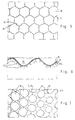
- Figure 1 shows an enlarged plan view of a Detail of the surface of a roller 1 in a predetermined grid R with truncated pyramid-shaped cups N is provided.
- A remains between the wells small bridge S and the inclined walls W itch in a flat floor B.
- Figure 2 shows a thousand times magnification of a small one Section of the wall W and the bottom B of one Cup N, which is made of a hard material HS, e.g. Stole, existing structure through a micrometer-thick doping with an ion implant material H and one overlying top layer D is provided.
- a hard material HS e.g. Stole
- H ion implant material
- Figure 3 shows an enlarged cross section in the Roll surface into it, the well N in known Way with an oxidic hard material HS from a There is a nickel matrix with a carbide insert on one Hard chrome layer is applied. The chrome surface is then by ion implantation with the implant material H and the top layer D.
- Figure 4 shows an enlarged surface of the Hard material layer HS, which is provided with hard chrome. It clearly show the grain boundaries, which are small Form microcracks M. These micro cracks are caused by the High voltage implant closed.
- Figure 5 shows another type of the known Roller surfaces in high magnification.
- a ceramized surface made of chromium oxide for example provided with a well N by lasering.
- the Laser beam is guided from well to well and melts the material with high energy and evaporates part of the same, so that the well N are formed.
- they are Crater edges solidified unevenly from the melt, and many microcracks M are visible there.
- microcracks are sufficient M to a great depth relative to the well structure solidified well surface. These micro cracks M are filled with the implant H.
- the top layer D is shown, in particular the compatibility the color with the surface influenced favorably and you have a given adhesion to the ink gives.
- the strengths of layers H and D are excessive shown.
- Figure 7 shows one from left to right at an angle Deep grinding of a lasered Hard material layer HS. It can be seen that the microcracks M also in the low-lying areas about radially from extend the N cup. These micro cracks are going through the ion implantation filled and sealed. Furthermore gives the implant material H, D a relatively smooth Cell surface.
Landscapes
- Chemical & Material Sciences (AREA)
- Metallurgy (AREA)
- Engineering & Computer Science (AREA)
- Materials Engineering (AREA)
- Mechanical Engineering (AREA)
- Inorganic Chemistry (AREA)
- Organic Chemistry (AREA)
- Chemical Kinetics & Catalysis (AREA)
- Inking, Control Or Cleaning Of Printing Machines (AREA)
- Physical Vapour Deposition (AREA)
- Rolls And Other Rotary Bodies (AREA)
- Treatments Of Macromolecular Shaped Articles (AREA)
- Pens And Brushes (AREA)
- Application Of Or Painting With Fluid Materials (AREA)
- Electrochromic Elements, Electrophoresis, Or Variable Reflection Or Absorption Elements (AREA)
Description
- Fig. 1
- zeigt eine vergrößerte Aufsicht auf eine gerasterte Walzenoberfläche;
- Fig. 2
- zeigt einen 1000-fach vergrößerten Schnitt durch das Gefüge unter einem geprägten Näpfchen;
- Fig. 3
- zeigt einen hochvergrößerten Schnitt durch ein Näpfchen mit einer Hartstoff-Metallmatrix-Beschichtung;
- Fig. 4
- zeigt in 100-facher Vergrößerung Mikrorisse entlang der Korngrenzen einer Walzenbeschichtung;
- Fig. 5
- zeigt eine Aufsicht 150-fach vergrößert auf eine gelaserte Hartkeramikoberfläche;
- Fig. 6
- zeigt einen Querschnitt zu Fig. 5 in 350-facher Vergrößerung;
- Fig. 7
- zeigt einen schräg in die Tiefe verlaufenden Anschliff zu Fig. 5.
Claims (17)
- Farbübertragungswalze (1) mit einer mechanisch oder durch Laserung eingebrachten Oberflächenstruktur aus Farbübertragungsnäpfchen (N) in einer mikroporösen, metallischen oder keramischen oder metallkeramischen Hartstoffschicht (HS),
dadurch gekennzeichnet, daß oberflächliche Mikrorisse (M) und Poren durch ein mit einem Hochspannungsplasma appliziertes Ionenimplantatmaterial (H) geschlossen sind. - Farbübertragungswalze nach Anspruch 1, dadurch gekennzeichnet, daß das Ionenimplantatmaterial (H) aus einem vierwertigen Stoff und mindestens einem Schwermetall besteht.
- Farbübertragungswalze nach Anspruch 2, dadurch gekennzeichnet, daß das Ionenimplantatmaterial (H) aus Titan und Molybdän im Verhältnis 70/30 bis 90/10 besteht.
- Farbübertragungswalze nach einem der vorstehenden Ansprüche, dadurch gekennzeichnet, daß das Ionenimplantatmaterial (H) mit einer verschleißfesten, dünnen Deckschicht (D) aus einem Hartstoff, insbesondere einem Metalloxid und/oder Metallnitrid, durch eine Ionenimplantation so belegt ist, daß die Deckschicht (D) eine vorgegebene Affinität zu einer mit der Druckwalze zu dosierenden Druckfarbe aufweist.
- Farbübertragungswalze nach Anspruch 4, dadurch gekennzeichnet, daß die Deckschicht (D) eine Stärke von 0,05 - 1 µm, bevorzugt 0,1 µm, hat.
- Farbübertragungswalze nach Anspruch 4 oder 5, dadurch gekennzeichnet, daß die Deckschicht (D) aus Zirkonoxid, Siliziumoxid, Silizium oder Kohlenstoff besteht.
- Farbübertragungswalze nach Anspruch 1, dadurch gekennzeichnet, daß die Harstoffschicht (HS) aus geschliffenem und gefinischtem Chromoxid (Cr2O3) einer Stärke von 100 - 150 µm besteht und die Näpfchen (N) durch eine Lasergravur eingebracht und gefinischt sind und danach das Ionenimplantatmaterial (H) porenschließend eingebracht ist.
- Farbübertragungswalze nach Anspruch 1, dadurch gekennzeichnet, daß die Hartstoffschicht (HS) aus einer plasmaabgeschiedenen Nickel-Chromlegierung 80/20 von ca. 100 µm Dicke besteht.
- Farbübertragungswalze nach Anspruch 1, dadurch gekennzeichnet, daß die Hartstoffschicht (HS) aus Stahl, Kupfer oder Nickel besteht, das nach dem Einbringen der Näpfchen (N) und elektrolytischer Polierung dünn mit Hartchrom (HC) beschichtet ist.
- Farbübertragungswalze nach Anspruch 1, dadurch gekennzeichnet, daß die Hartstoffschicht (HS) aus Stahl, Kupfer oder Nickel besteht, das nach dem Einbringen der Näpfchen (N) elektrolytisch mit einer Metallmatrix unter Einlagerung von Hartstoffkörnern beschichtet ist.
- Farbübertragungswalze nach Anspruch 10, dadurch gekennzeichnet, daß die Hartstoffkörner aus Siliciumcarbid bestehen und in einer Nickelmatrix eingelagert sind.
- Farbübertragungswalze nach einem der vorstehenden Ansprüche, dadurch gekennzeichnet, daß die Hartstoffschicht (HS) auf eine dünne metallische Zwischenschicht aufgebracht ist, die auf einem Kunststoffmantel, der Kunststofffasereinlagen enthält, aufgesputtert ist.
- Verfahren zu Herstellung einer hochabriebfesten und hochkorrosionsfesten Farbübertragungwalze, insbes. nach einem der vorstehenden Ansprüche, dadurch gekennzeichnet, daß die Walze (1) nach dem Einbringen der Näpfchen (N) in einem ersten Implantationsschritt in einem Gasentladungsplasma bei einer Spannung von eintausend Volt bis zu zehntausend Volt bei einer Temperatur zwischen 50 - 80°C einer turbulenten Schwermetallionen-Implantation ausgesetzt wird, bis Mikrorisse (M) und Mikroporen der Oberfläche aufgefüllt sind und auf freier Oberfläche das Ionenimplantatmaterial (H) in einer Schichtstärke unter 1 µm aufgewachsen ist.
- Verfahren nach Anspruch 13, dadurch gekennzeichnet, daß als Ionen vier- und sechswertige Stoffe, insbes. Titan und Molybdän in einem Gewichtsverhältnis von 70/30 bis 90/10, dem Plasma zugeführt werden.
- Verfahren nach Anspruch 13 oder 14, dadurch gekennzeichnet, daß die Gasentladung in Stickstoff oder Sauerstoff bei ca. 1 mbar Druck brennt.
- Verfahren nach einem der Ansprüche 13 bis 15, dadurch gekennzeichnet, daß dem ersten Implantationsschritt ein zweiter folgt, bei dem die Walze (1) in einem Gasentladungsplasma bei einer Spannung von eintausend bis zehntausend Volt mit einer Auftreffenergie von 600 - 2000 eV bei einer Temperatur zwischen 50 - 80°C einer turbulenten Metallionen, Metalloxid und/oder Metallnitrid-Implantation ausgesetzt wird, bis das Oxid oder Nitrid auf eine Schichtstärke von 0,05 bis 1 µm auf der Oberfläche aufgewachsen ist.
- Verfahren nach Anspruch 16, dadurch gekennzeichnet, daß aus dem Gasentladungsplasma Zirkonoxid (Zr02), Siliziumoxid, Silizium oder Kohlensotff implantiert wird.
Applications Claiming Priority (2)
| Application Number | Priority Date | Filing Date | Title |
|---|---|---|---|
| DE19516032 | 1995-05-04 | ||
| DE19516032A DE19516032C2 (de) | 1995-05-04 | 1995-05-04 | Verfahren zur Oberflächenveredelung einer Farbübertragungswalze durch Ionenimplantation |
Publications (3)
| Publication Number | Publication Date |
|---|---|
| EP0748701A2 EP0748701A2 (de) | 1996-12-18 |
| EP0748701A3 EP0748701A3 (de) | 1997-11-12 |
| EP0748701B1 true EP0748701B1 (de) | 1999-10-13 |
Family
ID=7760844
Family Applications (1)
| Application Number | Title | Priority Date | Filing Date |
|---|---|---|---|
| EP96107011A Expired - Lifetime EP0748701B1 (de) | 1995-05-04 | 1996-05-03 | Farbübertragungswalze mit Ionenimplantat |
Country Status (5)
| Country | Link |
|---|---|
| EP (1) | EP0748701B1 (de) |
| AT (1) | ATE185519T1 (de) |
| DE (2) | DE19516032C2 (de) |
| DK (1) | DK0748701T3 (de) |
| ES (1) | ES2138263T3 (de) |
Families Citing this family (12)
| Publication number | Priority date | Publication date | Assignee | Title |
|---|---|---|---|---|
| US6786153B2 (en) * | 2002-09-19 | 2004-09-07 | Interflex Laser Engravers, Llc | Printing rolls having wear indicators and methods for determining wear of printing and anilox rolls and sleeves |
| DE19840951A1 (de) * | 1998-09-08 | 2000-03-09 | Jagenberg Papiertech Gmbh | Rakelstange für eine Beschichtungsvorrichtung |
| DE10222453A1 (de) * | 2002-05-22 | 2003-12-04 | Voith Paper Patent Gmbh | Verfahren zur Oberflächenbehandlung eines Rakelelementes |
| DE102005030918A1 (de) * | 2005-06-30 | 2007-01-04 | Man Roland Druckmaschinen Ag | Farbduktorwalze einer Rollendruckmaschine |
| DE102005062527A1 (de) | 2005-12-16 | 2007-06-21 | Gebr. Schmid Gmbh & Co. | Vorrichtung und Verfahren zur Oberflächenbehandlung von Substraten |
| DE102005062528A1 (de) * | 2005-12-16 | 2007-06-21 | Gebr. Schmid Gmbh & Co. | Vorrichtung und Verfahren zur Oberflächenbehandlung von Substraten |
| DE102006003386A1 (de) * | 2006-01-24 | 2007-07-26 | Reichel, Walter, Dipl.-Ing. | Vorrichtung und Verfahren zur Oberflächenbehandlung von Walzen in der Papierindustrie |
| DE102006005120A1 (de) | 2006-02-04 | 2007-08-09 | Man Roland Druckmaschinen Ag | Farbduktorwalze einer Rollendruckmaschine |
| DE202009005879U1 (de) | 2009-04-22 | 2009-07-02 | Kurt Zecher Gmbh | Farbübertragungswalze für Druckmaschinen |
| CN107419234B (zh) * | 2017-07-22 | 2019-04-09 | 北京工商大学 | 一种耐磨抗菌的食品加工机械不锈钢部件及其制备工艺 |
| CN107385405B (zh) * | 2017-07-22 | 2019-04-09 | 北京工商大学 | 一种离子注入改性层深度可控的不锈钢部件及其制备工艺 |
| CN118380337B (zh) * | 2024-06-25 | 2024-09-06 | 日月新半导体(威海)有限公司 | 一种半导体晶片的封装结构及其形成方法 |
Family Cites Families (6)
| Publication number | Priority date | Publication date | Assignee | Title |
|---|---|---|---|---|
| JPS6044394A (ja) * | 1983-08-22 | 1985-03-09 | Mitsubishi Heavy Ind Ltd | インキロ−ラ |
| JPH07119151B2 (ja) * | 1987-12-07 | 1995-12-20 | 富士写真フイルム株式会社 | 平版印刷版用支持体 |
| EP0404973A1 (de) * | 1989-06-27 | 1991-01-02 | Hauzer Holding B.V. | Verfahren und Vorrichtung zur Beschichtung von Substraten |
| FI83439C (fi) * | 1989-08-24 | 1991-07-10 | Valmet Paper Machinery Inc | Vals i pappersmaskin och foerfarande foer framstaellning av denna. |
| DE4007130C1 (de) * | 1990-03-07 | 1991-06-27 | Kurt Zecher Gmbh, 4790 Paderborn, De | |
| DE4426485C1 (de) * | 1994-07-26 | 1995-11-30 | Zecher Gmbh Kurt | Farbübertragungswalze mit austauschbarem Bezug |
-
1995
- 1995-05-04 DE DE19516032A patent/DE19516032C2/de not_active Expired - Fee Related
-
1996
- 1996-05-03 DK DK96107011T patent/DK0748701T3/da active
- 1996-05-03 AT AT96107011T patent/ATE185519T1/de not_active IP Right Cessation
- 1996-05-03 ES ES96107011T patent/ES2138263T3/es not_active Expired - Lifetime
- 1996-05-03 EP EP96107011A patent/EP0748701B1/de not_active Expired - Lifetime
- 1996-05-03 DE DE59603324T patent/DE59603324D1/de not_active Expired - Fee Related
Also Published As
| Publication number | Publication date |
|---|---|
| DE19516032A1 (de) | 1996-11-07 |
| DK0748701T3 (da) | 2000-04-17 |
| EP0748701A3 (de) | 1997-11-12 |
| EP0748701A2 (de) | 1996-12-18 |
| DE19516032C2 (de) | 2001-03-01 |
| DE59603324D1 (de) | 1999-11-18 |
| ES2138263T3 (es) | 2000-01-01 |
| ATE185519T1 (de) | 1999-10-15 |
Similar Documents
| Publication | Publication Date | Title |
|---|---|---|
| EP1032721B1 (de) | Verschleissbeständiger, mechanisch hochbelastbarer und reibungsarmer randschichtaufbau für titan oder seine legierungen sowie verfahren zu seiner herstellung | |
| DE69825570T2 (de) | Verfahren zur herstellung von oxiden mit konstanter dicke auf zirconiumlegierungen | |
| EP1448908B1 (de) | Implantat | |
| DE4310896C1 (de) | Verfahren zum Herstellen von verschleißfesten Kanten an Turbinenschaufeln | |
| EP0925382B1 (de) | Verschleissbeständiger, mechanisch hochbelastbarer und reibungsarmer randschichtaufbau aus einem substrat aus titan oder seinen legierungen sowie verfahren zu seiner herstellung | |
| EP3155284A1 (de) | Bremsscheibe für ein kraftfahrzeug | |
| DE69016161T2 (de) | Walze für die Papiererzeugung und Verfahren zu deren Herstellung. | |
| EP0748701A2 (de) | Farbübertragungswalze mit Ionenimplantat | |
| DE2926879A1 (de) | Verfahren zum beschichten der oberflaeche von metallsubstraten mit verschleissfesten materialien | |
| DE2221875A1 (de) | Oberflaechengehaerteter und gesinterter karbid-formgegenstand | |
| WO2006005527A1 (de) | Verfahren zur herstellung von verschleissbeständigen und ermüdungsresistenten randschichten in titan-legierungen und damit hergestellte bauteile | |
| DE3640430C2 (de) | ||
| EP1192303B1 (de) | Ringläufer und verfahren zu dessen herstellung | |
| DE102009020674A1 (de) | Verfahren zum Herstellen eines beschichteten Bauteils | |
| DE3830848C1 (de) | ||
| DE1925486C3 (de) | Anwendung der lonitrierung auf Miniaturkugeln | |
| DE102010049840B4 (de) | Bauteil mit einer Verschleißschutzschicht | |
| DE10059903B4 (de) | Kolben mit Verschleißschutzschicht | |
| DE3212214C2 (de) | Kolbenring und Verfahren zu dessen Herstellung | |
| EP0884405B1 (de) | Verfahren zum Erzeugen harter Oxidschichten an der Oberfläche eines Substrats auf Basis von Leichtmetallen | |
| DE102015102966A1 (de) | Verfahren zum Herstellen einer Lauffläche für eine Dichtung | |
| JP4639317B2 (ja) | ロールの製造方法 | |
| DE19848025A1 (de) | Verfahren zur Oberflächenbehandlung von Werkzeugen und Werkzeuge mit behandelter Oberfläche | |
| EP4200533B1 (de) | Gleitlagerelement | |
| KR0173774B1 (ko) | 마모부품의 표면경화 방법 |
Legal Events
| Date | Code | Title | Description |
|---|---|---|---|
| PUAI | Public reference made under article 153(3) epc to a published international application that has entered the european phase |
Free format text: ORIGINAL CODE: 0009012 |
|
| AK | Designated contracting states |
Kind code of ref document: A2 Designated state(s): AT BE CH DE DK ES FI FR GB GR IE IT LI LU MC NL PT SE |
|
| PUAL | Search report despatched |
Free format text: ORIGINAL CODE: 0009013 |
|
| AK | Designated contracting states |
Kind code of ref document: A3 Designated state(s): AT BE CH DE DK ES FI FR GB GR IE IT LI LU MC NL PT SE |
|
| 17P | Request for examination filed |
Effective date: 19971120 |
|
| GRAG | Despatch of communication of intention to grant |
Free format text: ORIGINAL CODE: EPIDOS AGRA |
|
| 17Q | First examination report despatched |
Effective date: 19981130 |
|
| GRAG | Despatch of communication of intention to grant |
Free format text: ORIGINAL CODE: EPIDOS AGRA |
|
| GRAH | Despatch of communication of intention to grant a patent |
Free format text: ORIGINAL CODE: EPIDOS IGRA |
|
| GRAH | Despatch of communication of intention to grant a patent |
Free format text: ORIGINAL CODE: EPIDOS IGRA |
|
| GRAA | (expected) grant |
Free format text: ORIGINAL CODE: 0009210 |
|
| AK | Designated contracting states |
Kind code of ref document: B1 Designated state(s): AT BE CH DE DK ES FI FR GB GR IE IT LI LU MC NL PT SE |
|
| PG25 | Lapsed in a contracting state [announced via postgrant information from national office to epo] |
Ref country code: SE Free format text: THE PATENT HAS BEEN ANNULLED BY A DECISION OF A NATIONAL AUTHORITY Effective date: 19991013 Ref country code: GR Free format text: LAPSE BECAUSE OF NON-PAYMENT OF DUE FEES Effective date: 19991013 Ref country code: FI Free format text: LAPSE BECAUSE OF NON-PAYMENT OF DUE FEES Effective date: 19991013 |
|
| REF | Corresponds to: |
Ref document number: 185519 Country of ref document: AT Date of ref document: 19991015 Kind code of ref document: T |
|
| REG | Reference to a national code |
Ref country code: CH Ref legal event code: EP |
|
| REF | Corresponds to: |
Ref document number: 59603324 Country of ref document: DE Date of ref document: 19991118 |
|
| ITF | It: translation for a ep patent filed | ||
| ET | Fr: translation filed | ||
| REG | Reference to a national code |
Ref country code: ES Ref legal event code: FG2A Ref document number: 2138263 Country of ref document: ES Kind code of ref document: T3 |
|
| PG25 | Lapsed in a contracting state [announced via postgrant information from national office to epo] |
Ref country code: PT Free format text: LAPSE BECAUSE OF FAILURE TO SUBMIT A TRANSLATION OF THE DESCRIPTION OR TO PAY THE FEE WITHIN THE PRESCRIBED TIME-LIMIT Effective date: 20000113 |
|
| REG | Reference to a national code |
Ref country code: IE Ref legal event code: FG4D Free format text: GERMAN |
|
| GBT | Gb: translation of ep patent filed (gb section 77(6)(a)/1977) |
Effective date: 20000107 |
|
| REG | Reference to a national code |
Ref country code: DK Ref legal event code: T3 |
|
| PG25 | Lapsed in a contracting state [announced via postgrant information from national office to epo] |
Ref country code: LU Free format text: LAPSE BECAUSE OF NON-PAYMENT OF DUE FEES Effective date: 20000503 Ref country code: AT Free format text: LAPSE BECAUSE OF NON-PAYMENT OF DUE FEES Effective date: 20000503 |
|
| PG25 | Lapsed in a contracting state [announced via postgrant information from national office to epo] |
Ref country code: BE Free format text: LAPSE BECAUSE OF NON-PAYMENT OF DUE FEES Effective date: 20000531 |
|
| PLBE | No opposition filed within time limit |
Free format text: ORIGINAL CODE: 0009261 |
|
| STAA | Information on the status of an ep patent application or granted ep patent |
Free format text: STATUS: NO OPPOSITION FILED WITHIN TIME LIMIT |
|
| PG25 | Lapsed in a contracting state [announced via postgrant information from national office to epo] |
Ref country code: IE Free format text: LAPSE BECAUSE OF NON-PAYMENT OF DUE FEES Effective date: 20000816 |
|
| REG | Reference to a national code |
Ref country code: IE Ref legal event code: FD4D |
|
| 26N | No opposition filed | ||
| BERE | Be: lapsed |
Owner name: KURT ZECHER G.M.B.H. Effective date: 20000531 |
|
| PG25 | Lapsed in a contracting state [announced via postgrant information from national office to epo] |
Ref country code: MC Free format text: LAPSE BECAUSE OF NON-PAYMENT OF DUE FEES Effective date: 20001130 |
|
| REG | Reference to a national code |
Ref country code: GB Ref legal event code: IF02 |
|
| PGFP | Annual fee paid to national office [announced via postgrant information from national office to epo] |
Ref country code: FR Payment date: 20050428 Year of fee payment: 10 |
|
| PGFP | Annual fee paid to national office [announced via postgrant information from national office to epo] |
Ref country code: ES Payment date: 20050429 Year of fee payment: 10 |
|
| PGFP | Annual fee paid to national office [announced via postgrant information from national office to epo] |
Ref country code: GB Payment date: 20050503 Year of fee payment: 10 |
|
| PGFP | Annual fee paid to national office [announced via postgrant information from national office to epo] |
Ref country code: DK Payment date: 20050511 Year of fee payment: 10 |
|
| PGFP | Annual fee paid to national office [announced via postgrant information from national office to epo] |
Ref country code: NL Payment date: 20050516 Year of fee payment: 10 |
|
| PGFP | Annual fee paid to national office [announced via postgrant information from national office to epo] |
Ref country code: CH Payment date: 20050518 Year of fee payment: 10 |
|
| PGFP | Annual fee paid to national office [announced via postgrant information from national office to epo] |
Ref country code: DE Payment date: 20050527 Year of fee payment: 10 |
|
| PG25 | Lapsed in a contracting state [announced via postgrant information from national office to epo] |
Ref country code: GB Free format text: LAPSE BECAUSE OF NON-PAYMENT OF DUE FEES Effective date: 20060503 |
|
| PG25 | Lapsed in a contracting state [announced via postgrant information from national office to epo] |
Ref country code: ES Free format text: LAPSE BECAUSE OF NON-PAYMENT OF DUE FEES Effective date: 20060504 |
|
| PG25 | Lapsed in a contracting state [announced via postgrant information from national office to epo] |
Ref country code: LI Free format text: LAPSE BECAUSE OF NON-PAYMENT OF DUE FEES Effective date: 20060531 Ref country code: DK Free format text: LAPSE BECAUSE OF NON-PAYMENT OF DUE FEES Effective date: 20060531 Ref country code: CH Free format text: LAPSE BECAUSE OF NON-PAYMENT OF DUE FEES Effective date: 20060531 |
|
| PGFP | Annual fee paid to national office [announced via postgrant information from national office to epo] |
Ref country code: IT Payment date: 20060531 Year of fee payment: 11 |
|
| PG25 | Lapsed in a contracting state [announced via postgrant information from national office to epo] |
Ref country code: NL Free format text: LAPSE BECAUSE OF NON-PAYMENT OF DUE FEES Effective date: 20061201 Ref country code: DE Free format text: LAPSE BECAUSE OF NON-PAYMENT OF DUE FEES Effective date: 20061201 |
|
| REG | Reference to a national code |
Ref country code: CH Ref legal event code: PL Ref country code: DK Ref legal event code: EBP |
|
| GBPC | Gb: european patent ceased through non-payment of renewal fee |
Effective date: 20060503 |
|
| NLV4 | Nl: lapsed or anulled due to non-payment of the annual fee |
Effective date: 20061201 |
|
| REG | Reference to a national code |
Ref country code: FR Ref legal event code: ST Effective date: 20070131 |
|
| REG | Reference to a national code |
Ref country code: ES Ref legal event code: FD2A Effective date: 20060504 |
|
| PG25 | Lapsed in a contracting state [announced via postgrant information from national office to epo] |
Ref country code: FR Free format text: LAPSE BECAUSE OF NON-PAYMENT OF DUE FEES Effective date: 20060531 |
|
| PG25 | Lapsed in a contracting state [announced via postgrant information from national office to epo] |
Ref country code: IT Free format text: LAPSE BECAUSE OF NON-PAYMENT OF DUE FEES Effective date: 20070503 |