EP0740862B1 - Fliessband-analog-digital-wandler mit digitaler kurvenkorrekturabstimmung - Google Patents
Fliessband-analog-digital-wandler mit digitaler kurvenkorrekturabstimmung Download PDFInfo
- Publication number
- EP0740862B1 EP0740862B1 EP94929793A EP94929793A EP0740862B1 EP 0740862 B1 EP0740862 B1 EP 0740862B1 EP 94929793 A EP94929793 A EP 94929793A EP 94929793 A EP94929793 A EP 94929793A EP 0740862 B1 EP0740862 B1 EP 0740862B1
- Authority
- EP
- European Patent Office
- Prior art keywords
- digital
- stage
- error
- gain
- signal
- Prior art date
- Legal status (The legal status is an assumption and is not a legal conclusion. Google has not performed a legal analysis and makes no representation as to the accuracy of the status listed.)
- Expired - Lifetime
Links
Images


Classifications
-
- H—ELECTRICITY
- H03—ELECTRONIC CIRCUITRY
- H03M—CODING; DECODING; CODE CONVERSION IN GENERAL
- H03M1/00—Analogue/digital conversion; Digital/analogue conversion
- H03M1/10—Calibration or testing
- H03M1/1009—Calibration
- H03M1/1028—Calibration at two points of the transfer characteristic, i.e. by adjusting two reference values, e.g. offset and gain error
-
- H—ELECTRICITY
- H03—ELECTRONIC CIRCUITRY
- H03M—CODING; DECODING; CODE CONVERSION IN GENERAL
- H03M1/00—Analogue/digital conversion; Digital/analogue conversion
- H03M1/12—Analogue/digital converters
- H03M1/34—Analogue value compared with reference values
- H03M1/38—Analogue value compared with reference values sequentially only, e.g. successive approximation type
- H03M1/44—Sequential comparisons in series-connected stages with change in value of analogue signal
Definitions
- This invention pertains to analog-to-digital converters, and more specifically to pipelined analog-to-digital converters which, in accordance with the teachings of this invention, utilize digital correction features.
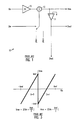
- the typical N-bit pipelined analog-to-digital converter (ADC) consists of N 1-bit stages which, as shown in Figure 1, each include a comparator 11, summing element 12, and gain element 13.
- the analog input signal Vin to stage 10 is multiplied by 2 by gain element 13.
- a reference voltage Vref is either added to or subtracted from 2*Vin by summing element 12, depending upon the digital input signal Din to stage 10.
- the resultant residual voltage Vres 2 Vin ⁇ Vref is applied the next stage.
- the polarity of residual voltage Vres is detected by comparator 11, whose output signal Dout serves as the digital input signal Din of the next stage.
- Cascading N similar stages 10-1 through 10-N results in an N-bit Analog-to-Digital converter, as shown in Figure 2, where the residual voltages of each stage are defined by equations (2), (3) and (4).
- stage 10-0 provides an N+1 bit ADC, which is the sign of the input voltage Vin.
- stage 10-0 includes a one-times multiplier (for example, just a wired connection), and a comparator.
- Vres 2 2( Vres 1 ⁇ Vref 2 )
- Vres N 2( Vres N -1 ⁇ Vref 2 )
- Equation 1 for an input voltage of Vin
- Equation 2 for an input voltage of Vin
- Figure 4a shows the ideal transfer function and the actual transfer function for a stage in which the gain factor of gain element 13 (Figure 1) is less than 2 as caused, for example, by capacitor mismatch
- Figure 4b shows the ideal and actual transfer functions for a stage in which the gain is greater than 2 as caused, for example, by capacitor mismatch
- Figure 4c shows the ideal and actual transfer function for a stage in which reference mismatch errors cause vertical shift
- Figure 4d shows the ideal and actual transfer functions of a stage in which charge injection in the comparator feedback switch causes a comparator offset.
- Gain element 13 includes an operational amplifier which inherently has finite gain and offset errors.
- Figure 5 is a graph having ADC code values (i.e., digital output words) on its X-axis, and the error, as measured in a multiple of the least significant bit value, displayed on its Y-axis. As shown in Figure 5, for the criteria established for this example, a maximum error of approximately 1200 LSB is the undesirable result.
- ADC code values i.e., digital output words
- Charge injection, gain, and reference errors can be removed by using known techniques, such as self-calibration techniques, trimming capacitor values and reference values, and the use of dummy devices to minimize charge injection.
- offset error and full scale error are determined by applying ⁇ Vref as an input signal to the ADC. These values allow the raw digital data from the ADC to be compensated in either hardware or software to provide a more accurate digital representation of the analog input voltage being measured.
- second order errors are removed by determining the magnitude of, for example, the error due to capacitor voltage coefficients of the MSB stage of the ADC after calibration of lesser significant bit stages, and using these voltage coefficients to further adjust the digital output word, providing an even more accurate digital representation of the analog input signal being measured.
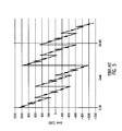
- a second characteristic of a pipelined ADC is the inherent analog "multimeter" contained within the pipe. For the moment, consider a 16-bit ADC (having stages 10-0 through 10-16), in which stage 10-1 is non-ideal with a constant gain error and an associated residual voltage error as shown in Figure 8a, while all remaining stages (stages 10-2 through 10-16) are ideal. A linearity sweep of an ADC under these conditions, as shown in Figure 12, results in linearity errors whose signature matches the signature of the non-ideal stage 10-1, as depicted in the graph of Figure 8b. This inherent feature of pipelined ADCs allows calibration of a given stage once stages for less significant bits have been calibrated.
- the ADC offset and ADC gain errors are determined.
- Digital correction terms are generated by applying +Vref to the ADC to measure the ADC fullscale error and by applying -Vref to measure the ADC offset error.
- the second correction term, offset allows for adjustment of the offset of the linearity, for example by using an adder.
- the raw digital output Dout(raw) is modified using gain and offset correction factors, as shown by Equations 11 and 12.
- Dout 1 Dout ( raw ) -offset and following this step,
- Dout ( g/o corrected ) Dout 1 - Dout 1 x gain
- Dout(g/o corrected) is a digital output word including correction for gain and offset errors.
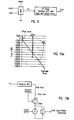
- Figure 10b is a block diagram of a structure in accordance with the teachings of this invention suitable for implementing the correction factors exemplified by equations (11) and (12).
- Figure 9 depicts how MSB stage 10-1 is calibrated in accordance with the teachings of thus invention for removing the "system gain” and system offset” errors.
- stages 10-2 through 10-N were previously calibrated, for example by using techniques known in the prior art as well as the offset and gain calibration of this invention as described above, they may be used to measure the linearity of the first stage, stage 10-1 and the ADC gain error and ADC offset error.
- a capacitor voltage coefficient error on the first stage results in a hyperbolic type transfer function in the linearity plot.
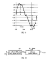
- This hyperbola has its vertices at ⁇ Vref/2, which, for a typical ADC operating with a Vcc of 5 volts, and thus using a Vref of 5 volts, this hyperbola has its vertices at approximately plus and minus 2.5 volts, as shown in Figure 11.
- output:+Vref/2 is equal to 49152 and the digital value of the sign bit is equal to 32768, and thus the value of output:+Vref/2 - sign bit is equal to 16384.
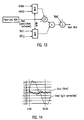
- Figure 14 is a graph depicting a first curve Dout(g/o correction) showing a rather significant second order voltage coefficient existing after gain and offset calibration as taught by the present invention, but prior to second order calibration.
- the second curve Dout(final) of Figure 14 shows the much improved second order voltage coefficient resulting from second order calibration in accordance with the teachings of this invention.
- Second order calibration with linear gain and offset calibration, improves the total unadjusted error to 1/4 LSB accuracy with no offset or fullscale error.
Landscapes
- Engineering & Computer Science (AREA)
- Theoretical Computer Science (AREA)
- Analogue/Digital Conversion (AREA)
Claims (3)
- Verfahren zum Kalibrieren eines Pipeline-Analog/Digital-Wandlers mit einer Mehrzahl Stufen (10-0, 10-1), in jeder von denen ein jeweiliges Eingabesignal mit einem Bezugssignal (Vref) verglichen wird, um ein jeweiliges Bit eines Ausgabedigitalworts zu liefern, und wobei ein Eingabesignal für die nächste signifikante Stufe durch Verstärken entweder der Summe oder der Differenz zwischen dem jeweiligen Eingabesignal und dem Bezugssignal gebildet wird,
dadurch gekennzeichnet, daß ein dem Bezugssignal entsprechends erstes Signal als Eingabesignal an eine signifikanteste Stufe angelegt wird, um ein erstes Digitalausgabewort zu liefern, das den Offset-Fehler einer oder mehrerer nichtkalibrierter signifikanterer Stufen anzeigt, und wobei ein zweites Signal, das in der Amplitude gleich und im Vorzeichen entgegengesetzt zu dem ersten Signal ist, als ein Eingabesignal an die signifikanteste Stufe angelegt wird, um ein zweites Digitalausgabewort zu liefern, das den Verstärkungsfehler einer oder mehrere unkalibrierter signifikanteterer Stufen anzeigt. - Verfahren nach Anspruch 1,
bei dem weniger signifikanten Stufen des Wandlers kalibriert werden, bevor die ersten und zweiten Signale angelegt werden. - Verfahren nach Anspruch 1 oder Anspruch 2,
bei dem ein der Hälfte des Referenzsignals entsprechendes drittes Signal und ein viertes Signal, das in der Amplitude gleich und im Vorzeichen entgegengesetzt zu dem dritten Signal ist, als Eingabesignale an die signifikanteste Stufe angelegt werden, um einen Fehlerkoeffizienten zweiter Ordnung zu bestimmen.
Applications Claiming Priority (3)
| Application Number | Priority Date | Filing Date | Title |
|---|---|---|---|
| US08/183,679 US5465092A (en) | 1994-01-19 | 1994-01-19 | Pipelined analog-to-digital converter with curvefit digital correction |
| US183679 | 1994-01-19 | ||
| PCT/US1994/010318 WO1995020270A1 (en) | 1994-01-19 | 1994-09-12 | Pipelined analog-to-digital converter with curvefit digital correction |
Publications (2)
| Publication Number | Publication Date |
|---|---|
| EP0740862A1 EP0740862A1 (de) | 1996-11-06 |
| EP0740862B1 true EP0740862B1 (de) | 1998-10-28 |
Family
ID=22673860
Family Applications (1)
| Application Number | Title | Priority Date | Filing Date |
|---|---|---|---|
| EP94929793A Expired - Lifetime EP0740862B1 (de) | 1994-01-19 | 1994-09-12 | Fliessband-analog-digital-wandler mit digitaler kurvenkorrekturabstimmung |
Country Status (4)
| Country | Link |
|---|---|
| US (1) | US5465092A (de) |
| EP (1) | EP0740862B1 (de) |
| DE (1) | DE69414271T2 (de) |
| WO (1) | WO1995020270A1 (de) |
Families Citing this family (33)
| Publication number | Priority date | Publication date | Assignee | Title |
|---|---|---|---|---|
| EP0730794B1 (de) * | 1994-09-23 | 2000-06-07 | National Semiconductor Corporation | Effiziente architektur zur korrektur von komponentenfehlanpassungen und schaltungsnichtlinearitäten in a/d umsetzern |
| US6694163B1 (en) | 1994-10-27 | 2004-02-17 | Wake Forest University Health Sciences | Method and system for producing interactive, three-dimensional renderings of selected body organs having hollow lumens to enable simulated movement through the lumen |
| US5782762A (en) * | 1994-10-27 | 1998-07-21 | Wake Forest University | Method and system for producing interactive, three-dimensional renderings of selected body organs having hollow lumens to enable simulated movement through the lumen |
| US5920319A (en) | 1994-10-27 | 1999-07-06 | Wake Forest University | Automatic analysis in virtual endoscopy |
| US5598157A (en) * | 1994-10-28 | 1997-01-28 | Harris Corporation | Sigma Delta analog to digital converter with three point calibration apparatus and method |
| US5739781A (en) * | 1996-10-08 | 1998-04-14 | National Semiconductor Corporation | Sub-ranging analog-to-digital converter with open-loop differential amplifiers |
| US5861826A (en) * | 1997-06-30 | 1999-01-19 | Harris Corporation | Method and apparatus for calibrating integrated circuit analog-to-digital converters |
| EP0930715A3 (de) * | 1998-01-15 | 2001-01-17 | Texas Instruments Incorporated | Digitales Selbstkalibriersystem für einen Fliessband-A/D-Wandler |
| US6222471B1 (en) * | 1998-01-15 | 2001-04-24 | Texas Instruments Incorporated | Digital self-calibration scheme for a pipelined A/D converter |
| US6222477B1 (en) * | 1998-06-16 | 2001-04-24 | Yokogawa Electric Corporation | Cascade A/D converter |
| US6417797B1 (en) | 1998-07-14 | 2002-07-09 | Cirrus Logic, Inc. | System for A multi-purpose portable imaging device and methods for using same |
| US6351228B1 (en) * | 1999-02-03 | 2002-02-26 | Hitachi Electronics Engineering Co., Ltd. | Digital calibration method and apparatus for A/D or D/A converters |
| SE514770C2 (sv) * | 1999-05-25 | 2001-04-23 | Ericsson Telefon Ab L M | Förfarande och arrangemang för korrigering av offsetfel vid A/D-omvandling |
| US6633618B1 (en) * | 1999-12-07 | 2003-10-14 | Nokia Corporation | Method and apparatus for digitally removing a DC-offset smaller than one LSB |
| US6445319B1 (en) | 2000-05-10 | 2002-09-03 | Texas Instruments Incorporated | Analog to digital converter circuit |
| JP2001352243A (ja) * | 2000-06-08 | 2001-12-21 | Fujitsu Ltd | A/d変換器及びa/d変換方法 |
| US6489904B1 (en) | 2001-07-27 | 2002-12-03 | Fairchild Semiconductor Corporation | Pipeline analog-to-digital converter with on-chip digital calibration |
| US6781531B2 (en) * | 2002-01-15 | 2004-08-24 | Raytheon Company | Statistically based cascaded analog-to-digital converter calibration technique |
| US6720895B2 (en) | 2002-02-01 | 2004-04-13 | Agilent Technologies, Inc. | Method of calibrating an analog-to-digital converter and a circuit implementing the same |
| JP2003242049A (ja) * | 2002-02-18 | 2003-08-29 | Niles Parts Co Ltd | マイクロコンピュータの異常検出方法 |
| US7106231B2 (en) * | 2003-11-04 | 2006-09-12 | Mstar Semiconductor, Inc. | Video signal processing system including analog to digital converter and related method for calibrating analog to digital converter |
| JP4320732B2 (ja) * | 2004-01-26 | 2009-08-26 | 横河電機株式会社 | カスケードa/d変換器 |
| TWI228876B (en) * | 2004-04-12 | 2005-03-01 | Realtek Semiconductor Corp | Error measurement method of digitally self-calibrating pipeline ADC and apparatus thereof |
| GB0423011D0 (en) * | 2004-10-16 | 2004-11-17 | Koninkl Philips Electronics Nv | Method and apparatus for analogue to digital conversion |
| KR100845134B1 (ko) * | 2006-11-06 | 2008-07-09 | 삼성전자주식회사 | 디지털 자동 보정기능을 가지는 파이프 라인아날로그-디지털 변환기 및 그것의 디지털 보정방법 |
| US7595748B2 (en) * | 2007-07-23 | 2009-09-29 | Mediatek Inc. | Method of gain error calibration in a pipelined analog-to-digital converter or a cyclic analog-to-digital converter |
| JP5517898B2 (ja) * | 2010-11-26 | 2014-06-11 | 株式会社日立製作所 | アナログデジタル変換器 |
| US8344920B1 (en) | 2011-09-29 | 2013-01-01 | Hittite Microwave Norway As | Methods and apparatus for calibrating pipeline analog-to-digital converters |
| US8941518B2 (en) | 2012-02-14 | 2015-01-27 | Hittite Microwave Corporation | Methods and apparatus for calibrating pipeline analog-to-digital converters having multiple channels |
| US8736471B2 (en) | 2012-08-22 | 2014-05-27 | Hittite Microwave Corporation | Methods and apparatus for calibrating stages in pipeline analog-to-digital converters |
| CN110531296B (zh) * | 2019-08-09 | 2022-05-10 | 格威半导体(厦门)有限公司 | 电池管理系统的增益校准方法 |
| US12231138B2 (en) * | 2023-06-06 | 2025-02-18 | Caelus Technologies Limited | Analog-to-digital converter (ADC) with reference ADC path receiving attenuated input to generate error codes for second and third harmonics by counting negative and positive codes |
| CN119449030B (zh) * | 2024-08-30 | 2025-11-07 | 泰为微电子(珠海)有限公司 | Adc实时校准装置、adc实时校准装置的控制方法和电子设备 |
Family Cites Families (5)
| Publication number | Priority date | Publication date | Assignee | Title |
|---|---|---|---|---|
| US4931797A (en) * | 1987-11-11 | 1990-06-05 | Matsushita Electric Industrial Co., Ltd. | Folding circuit and serial-type A/D converter |
| US4947168A (en) * | 1988-05-23 | 1990-08-07 | Hughes Aircraft Company | Subranging analog-to-digital converter with calibration |
| US5047772A (en) * | 1990-06-04 | 1991-09-10 | General Electric Company | Digital error correction system for subranging analog-to-digital converters |
| US5266952A (en) * | 1992-03-30 | 1993-11-30 | Hughes Aircraft Company | Feed forward predictive analog-to-digital converter |
| US5257026A (en) * | 1992-04-17 | 1993-10-26 | Crystal Semiconductor, Inc. | Method and apparatus for calibrating a multi-bit delta-sigma modular |
-
1994
- 1994-01-19 US US08/183,679 patent/US5465092A/en not_active Expired - Lifetime
- 1994-09-12 EP EP94929793A patent/EP0740862B1/de not_active Expired - Lifetime
- 1994-09-12 WO PCT/US1994/010318 patent/WO1995020270A1/en not_active Ceased
- 1994-09-12 DE DE69414271T patent/DE69414271T2/de not_active Expired - Lifetime
Also Published As
| Publication number | Publication date |
|---|---|
| EP0740862A1 (de) | 1996-11-06 |
| US5465092A (en) | 1995-11-07 |
| DE69414271D1 (de) | 1998-12-03 |
| WO1995020270A1 (en) | 1995-07-27 |
| DE69414271T2 (de) | 1999-06-02 |
Similar Documents
| Publication | Publication Date | Title |
|---|---|---|
| EP0740862B1 (de) | Fliessband-analog-digital-wandler mit digitaler kurvenkorrekturabstimmung | |
| US20020014982A1 (en) | A/D converter calibration | |
| US7187310B2 (en) | Circuit calibration using voltage injection | |
| US6222471B1 (en) | Digital self-calibration scheme for a pipelined A/D converter | |
| US6184809B1 (en) | User transparent self-calibration technique for pipelined ADC architecture | |
| US5635937A (en) | Pipelined multi-stage analog-to-digital converter | |
| JP3224808B2 (ja) | 冗長性a‐dおよびd‐a変換器の較正方法 | |
| US8094057B2 (en) | A/D conversion circuit, electronic apparatus, and A/D conversion method | |
| KR100332243B1 (ko) | 파이프라인형아날로그-디지탈변환기용기수2아키텍쳐및교정기법 | |
| US8344920B1 (en) | Methods and apparatus for calibrating pipeline analog-to-digital converters | |
| US7755521B1 (en) | A-D convert apparatus, D-A convert apparatus and adjustment method | |
| EP0730794B1 (de) | Effiziente architektur zur korrektur von komponentenfehlanpassungen und schaltungsnichtlinearitäten in a/d umsetzern | |
| US8742961B2 (en) | Gain and dither capacitor calibration in pipeline analog-to-digital converter stages | |
| US20030063026A1 (en) | Switched-capacitor based charge redistribution successive approximation analog to digital converter (ADC) | |
| US9882575B1 (en) | Analog-to-digital converter with offset calibration | |
| US5926123A (en) | Self calibration circuitry and algorithm for multipass analog to digital converter interstage gain correction | |
| US20030184464A1 (en) | Analog-to-digital conversion using an increased input range | |
| US6259392B1 (en) | Multiplying digital-to-analog converters and methods that selectively connect unit and feedback capacitors to reference voltages and feedback voltages | |
| US5173698A (en) | Flash analog-to-digital converter with integrating input stage | |
| US20030098808A1 (en) | Differential input A/D converter | |
| JP2002500460A (ja) | 暗黙利得配分によるアナログ−デジタル変換器のデジタル校正 | |
| US6198423B1 (en) | Analog-to-digital converter system having enhanced digital self-calibration | |
| Chang et al. | Radix-based digital calibration technique for multi-stage ADC | |
| EP1473836B1 (de) | Techniken zur Selbstkalibrierung im Digitalbereich und für den eingebauten Selbsttest von integrierten Hochgeschwindigkeits-A/D-Wandlern mit Hilfe von weissen Gauss-Geräuschen | |
| JPS5912619A (ja) | アナログ・デイジタル変換器の自動補正方法 |
Legal Events
| Date | Code | Title | Description |
|---|---|---|---|
| PUAI | Public reference made under article 153(3) epc to a published international application that has entered the european phase |
Free format text: ORIGINAL CODE: 0009012 |
|
| 17P | Request for examination filed |
Effective date: 19960816 |
|
| AK | Designated contracting states |
Kind code of ref document: A1 Designated state(s): DE FR GB |
|
| GRAG | Despatch of communication of intention to grant |
Free format text: ORIGINAL CODE: EPIDOS AGRA |
|
| 17Q | First examination report despatched |
Effective date: 19971124 |
|
| GRAG | Despatch of communication of intention to grant |
Free format text: ORIGINAL CODE: EPIDOS AGRA |
|
| GRAH | Despatch of communication of intention to grant a patent |
Free format text: ORIGINAL CODE: EPIDOS IGRA |
|
| GRAH | Despatch of communication of intention to grant a patent |
Free format text: ORIGINAL CODE: EPIDOS IGRA |
|
| GRAA | (expected) grant |
Free format text: ORIGINAL CODE: 0009210 |
|
| AK | Designated contracting states |
Kind code of ref document: B1 Designated state(s): DE FR GB |
|
| PG25 | Lapsed in a contracting state [announced via postgrant information from national office to epo] |
Ref country code: FR Free format text: LAPSE BECAUSE OF FAILURE TO SUBMIT A TRANSLATION OF THE DESCRIPTION OR TO PAY THE FEE WITHIN THE PRESCRIBED TIME-LIMIT Effective date: 19981028 |
|
| REF | Corresponds to: |
Ref document number: 69414271 Country of ref document: DE Date of ref document: 19981203 |
|
| EN | Fr: translation not filed | ||
| PLBE | No opposition filed within time limit |
Free format text: ORIGINAL CODE: 0009261 |
|
| STAA | Information on the status of an ep patent application or granted ep patent |
Free format text: STATUS: NO OPPOSITION FILED WITHIN TIME LIMIT |
|
| PG25 | Lapsed in a contracting state [announced via postgrant information from national office to epo] |
Ref country code: GB Free format text: LAPSE BECAUSE OF NON-PAYMENT OF DUE FEES Effective date: 19990912 |
|
| 26N | No opposition filed | ||
| GBPC | Gb: european patent ceased through non-payment of renewal fee |
Effective date: 19990912 |
|
| PGFP | Annual fee paid to national office [announced via postgrant information from national office to epo] |
Ref country code: DE Payment date: 20100929 Year of fee payment: 17 |
|
| REG | Reference to a national code |
Ref country code: DE Ref legal event code: R119 Ref document number: 69414271 Country of ref document: DE Effective date: 20130403 |
|
| PG25 | Lapsed in a contracting state [announced via postgrant information from national office to epo] |
Ref country code: DE Free format text: LAPSE BECAUSE OF NON-PAYMENT OF DUE FEES Effective date: 20130403 |