EP1473836B1 - Techniken zur Selbstkalibrierung im Digitalbereich und für den eingebauten Selbsttest von integrierten Hochgeschwindigkeits-A/D-Wandlern mit Hilfe von weissen Gauss-Geräuschen - Google Patents
Techniken zur Selbstkalibrierung im Digitalbereich und für den eingebauten Selbsttest von integrierten Hochgeschwindigkeits-A/D-Wandlern mit Hilfe von weissen Gauss-Geräuschen Download PDFInfo
- Publication number
- EP1473836B1 EP1473836B1 EP03398002A EP03398002A EP1473836B1 EP 1473836 B1 EP1473836 B1 EP 1473836B1 EP 03398002 A EP03398002 A EP 03398002A EP 03398002 A EP03398002 A EP 03398002A EP 1473836 B1 EP1473836 B1 EP 1473836B1
- Authority
- EP
- European Patent Office
- Prior art keywords
- self
- adc
- digital
- wgn
- calibration
- Prior art date
- Legal status (The legal status is an assumption and is not a legal conclusion. Google has not performed a legal analysis and makes no representation as to the accuracy of the status listed.)
- Expired - Lifetime
Links
Images


Classifications
-
- H—ELECTRICITY
- H03—ELECTRONIC CIRCUITRY
- H03M—CODING; DECODING; CODE CONVERSION IN GENERAL
- H03M1/00—Analogue/digital conversion; Digital/analogue conversion
- H03M1/10—Calibration or testing
- H03M1/1071—Measuring or testing
- H03M1/108—Converters having special provisions for facilitating access for testing purposes
-
- H—ELECTRICITY
- H03—ELECTRONIC CIRCUITRY
- H03M—CODING; DECODING; CODE CONVERSION IN GENERAL
- H03M1/00—Analogue/digital conversion; Digital/analogue conversion
- H03M1/10—Calibration or testing
- H03M1/1009—Calibration
- H03M1/1033—Calibration over the full range of the converter, e.g. for correcting differential non-linearity
- H03M1/1038—Calibration over the full range of the converter, e.g. for correcting differential non-linearity by storing corrected or correction values in one or more digital look-up tables
-
- H—ELECTRICITY
- H03—ELECTRONIC CIRCUITRY
- H03M—CODING; DECODING; CODE CONVERSION IN GENERAL
- H03M1/00—Analogue/digital conversion; Digital/analogue conversion
- H03M1/12—Analogue/digital converters
- H03M1/14—Conversion in steps with each step involving the same or a different conversion means and delivering more than one bit
- H03M1/16—Conversion in steps with each step involving the same or a different conversion means and delivering more than one bit with scale factor modification, i.e. by changing the amplification between the steps
- H03M1/164—Conversion in steps with each step involving the same or a different conversion means and delivering more than one bit with scale factor modification, i.e. by changing the amplification between the steps the steps being performed sequentially in series-connected stages
- H03M1/167—Conversion in steps with each step involving the same or a different conversion means and delivering more than one bit with scale factor modification, i.e. by changing the amplification between the steps the steps being performed sequentially in series-connected stages all stages comprising simultaneous converters
Definitions
- the present invention relates generally to integrated circuits, and particularly to a self-calibration technique employed in the design of high-speed analog-to-digital converters (ADC).
- ADC analog-to-digital converters
- the present invention can additionally be utilized as a cost-effective built-in self-testing (BIST) solution.
- ADCs Analog-to-Digital converters
- This linearity can be enhanced by way of component trimming or self-calibration techniques. Since trimming components is considered an expensive solution, self-calibration methods either in the analogue or in the digital domain are commonly considered for extending the resolution as well as the linearity of such ADCs above the 10-bit level.
- high-speed refers to conversion rates higher than Mega-Samples per second (MS/s).
- MS/s Mega-Samples per second
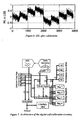
- a generic N -bit high-speed pipelined ADC architecture consists of a front-end input sample-and-hold (S/H), followed by a cascade of N S pipelined stages as shown in Figure 1. Each stage employs a flash quantizer and a multiplying digital-to-analogue converter (MDAC) that also performs the sample-and-hold function.
- MDAC multiplying digital-to-analogue converter
- a generic stage j processes the input signal in two phases and it is responsible for the extraction of M j bits. In the sampling phase, the input voltage is sampled and the corresponding value is stored in the MDAC, while a M j quantization is performed by the flash quantizer.
- This amplified residue, v raj is then held and applied to the next stage where identical operations are performed.
- the overall linearity is mainly limited by the mismatches in the first (front-end) MDAC.
- a typical conversion characteristic consists basically of 2 M l segments dislocated from an ideal straight-line.
- the gain-error of the MDAC affects the slope of these segments and is added to the jumps between two segments.
- a slightly lower than radix 2 inter-stage gain should be used in the first MDAC, because the gain-error resulting when the residue exceeds the allowed range can not be corrected by any digital technique [6]. This slightly reduces the full-scale range of the entire ADC, but ensures a successful self-calibration.
- the digital amounts of displacement can be measured during a calibration cycle and stored in a memory. Because fully differential MDACs exhibit code error symmetry, only one half of the calibrating-codes have to be calculated. These 2 ( M 1 -1) calibrating-codes can be later addressed and recalled during normal conversion mode, using the coarse digital outputs from the first stage M1 -bit quantizer. The conversion characteristic is then moved back to the ideal line (minus the reduced gain) by digitally subtracting these codes.
- a digital-domain self-calibration method is disclosed in "Electronics Letters, IEE, STEVENAGE, GB, vol. 38, no. 19, 12 September 2002, pages 1100-1101, XP006019051, GOES, J ET AL: "Digital-domain self calibration technique for video-rate pipeline A/D converters using Gaussian white noise".
- the present invention is a design technique for self-calibrating the linearity of high-speed analog-to-digital converters (ADC).
- ADC analog-to-digital converters
- the present invention consists in applying a WGN analog stimulus at the ADC input and calculating the calibrating codes from the histogram of the output codes by way of a truncated on-chip read-only memory (ROM) table.
- ROM read-only memory
- BIST on-chip high-speed built-in self-testing
- a (2 (M 1 -1) +1) bin histogram 3 can be computed by counting the number of occurrences of the output-codes inside these bins. Each bin covers a range of output codes that contain one expected step in the transfer characteristic. This histogram, H [i], will have a Gaussian-shape, which will be distorted by the existing deviations of the segments. 3 - Each bin in the histogram represents an interval of output digital codes of the ADC. The measured histogram represents, for all bins, the sum of the occurrences of the output codes comprised in each bin.
- T [ i ] ( A [ i ] ) ⁇ 1
- a [ i ] ⁇ C bin ( i ) ⁇ binwidth 2 C bin ( i ) + binwidth 2 ( ⁇ ⁇ 2 ⁇ ) ⁇ 1 e ⁇ ( x ⁇ ⁇ ) 2 2 ⁇ 2 d x
- C bin is the center of the bin
- T[ i ] is used to normalize H[ i ], resulting in the ideal case in a uniformly distributed histogram with 2 n occurrences in each bin.
- the differences from this expected value can be used to calculate the calibrating-codes in 4 steps:
- An accuracy of 1/16 LSB@ N -bit with a yield 3 ⁇ has to be reached to limit accumulated measurement errors below 1/2 LSB. To ensure this, the outermost bins representing the worst case are used to calculate the minimum number of samples.
- the number of samples needed to adjust the offset and the standard deviation of the WGN generator is calculated in the same way but using different bins and accuracy limits.
- the required accuracy concerning the statistical properties of the WGN stimulus depends mainly on the size of the bins.
- the standard deviation ⁇ has a linear influence on the measured transition voltages [8] and on the non-linearities. Because the measurement errors due to an imperfectly adjusted ⁇ accumulate over the observed code range, it is an advantage to use narrow bins at the code transitions of interest.
- ⁇ max ⁇ BIN ⁇ 2 N binwidth
- a binwidth of 64 bits and a required ⁇ BIN ⁇ 1/16 LSB allow the use of a 9-bit accurate ⁇ to calibrate a 12-bit ADC.
- a 14-bit ADC it would be required to use at least an 11-bit accurate ⁇ . Therefore, the efficiency of this technique is mainly limited by the ⁇ accuracy in the WGN generator. This accuracy can be easily adjusted during the generator setup using a digitally programmable gain amplifier (DPGA) together with a traditional successive-approximation algorithm.
- DPGA digitally programmable gain amplifier
- the offset in the WGN and in the ADC should also be calibrated digitally during the generator setup. This is sufficient to ensure that the subsequent steps of the calibration of the ADC do not fail.
- the wide-band WGN generator can be included on-chip by way of a high closed-loop gain amplifier with small input transistors and resistors employed as main noise sources. A detailed description of such circuits can be found in [8]. In fact, the input noise stimulus does not need to be necessarily white as long as it remains Gaussian.
- a 12-bit pipeline ADC employing the architecture presented in Figure 2 has been modeled at a functional level.
- This pipeline ADC consists in an input front-end sample-and-hold (S&H), in a 3-bit front-end stage comprising a 3-bit MDAC and a 3-bit flash quantizer and in a 10-bit ideal multi-stage pipeline backend ADC.
- Standard digital correction logic was included and the algorithm was implemented in the digital self-calibration circuitry block.
- the main static non-ideal effects were included, namely the offset voltages in the comparators of the flash quantizers and the limited matching accuracy (9-bit) in the capacitor-arrays in all MDAC blocks.
- the gain of the 3-bit front-end MDAC was nominally set to 3.9.
- the input-referred thermal noise of the ADC was also included and defined at 0.5 LSB below the quantization noise.
- An amount of n 2 24 samples was used to compute the histogram H [ i ] with 7 bins. This number of samples is sufficient for adjusting the WGN-generator and performing the self-calibration.
- the standard deviation of the WGN was set to ⁇ 2 ⁇ at full-scale plus the maximal allowed error.
- Figures 3 and 6 show, respectively, the INL of the ADC before and after calibration, measured using a static method by sweeping the input of the ADC with a full-scale ramp with steps of 1/8 LSB at 12-bit. After calibration, the initial INL of +4.5/-4.0 LSB is improved within the range of ⁇ 1LSB.
- Several simulations were carried-out with variations of the WGN generator offsets between ⁇ 8 mV.
- the resulting maximum INL errors after calibration were always within ⁇ 1 LSB, since about 1-bit is lost due to the accumulation of the digital truncation errors.
- the circuit depicted in Figure 7 is used to efficiently implement the digital self-calibration algorithm for the case of a 12 bit pipeline ADC.
- This circuit can be modified to implement the algorithm either for a different architecture of ADC or for a different ADC resolution.
- the 12-bit adder performs the correction using the calibrating-codes that are saved in 4 registers (C1 to C4). To reduce the number of required code-registers, the most significant bit of the ADC output decides if the codes are added or subtracted. Calibrating-codes with seven bit lengths allow for the correction of nonlinearities up to 128 LSB, including the corrections enforced by the reduced inter-stage gain.
- the offset register (OFF) and the gain adjustment register ( ⁇ ) are set during the initial calibration of the WGN generator using a similar method.
- the offset is then subtracted from the calibrating codes before the next histogram is taken, to ensure a symmetric behavior of the system after the WGN generator setup.
- the working registers (Reg 1 to Reg 4) contain the normalized values of the histogram bins. All the subsequent calculations such as subtractions and scaling can be done within these registers. As soon as the calculations described in section (A) (expressions 2 to 4) are accomplished, the working registers contain the new calibrating-codes and the calibrating-code registers are updated.
- Normalization factors stored in a ROM are employed, which are accumulated in the working registers every time a sample falls into the corresponding bin. This avoids the multiplication needed to normalize the histogram (2). All divisions to scale the calibrating-codes are radix 2 divisions, so they can be performed as a shift operation when the codes are written into the code registers. The 7 bit lines of the code registers are connected to the bus at the right position, so no additional shift unit is needed.
- the advantage of this system resides in its ability to perform multi-step calibration because already existing codes are used for new histograms but are not affected until they are updated.
Landscapes
- Engineering & Computer Science (AREA)
- Theoretical Computer Science (AREA)
- Physics & Mathematics (AREA)
- Nonlinear Science (AREA)
- Analogue/Digital Conversion (AREA)
Claims (5)
- Eine digitale Selbstkalibrierungsmethode für schnelle integrierte Analog-Digitalumsetzer (ADU) basierend auf gaussverteiltem weißen Rauschen (WGN) als Eingangsstimulus. Die hier beschriebene Methode besteht aus:a) Anlegen eines WGN Stimulus an den Eingang des ADU;b) Erzeugung eines digitalen Histogramms am Ausgang;c) Berechnung der Kalibrierungscodes von diesem digitalen Histogramm durch Anwendung einer im Speicher liegenden Tabelle (ROM), die das ideale Histogramm enthält, und durch einen 4-Schritt Algorithmus,dadurch gekennzeichnet,i) daß die ROM Tabelle, T[i], 2(M1-1) + 1 Werte verwendet, definiert durch:
 ii) daß die Sprünge durch Nichtlinearitäten (D[i]) berechnet werden mit:
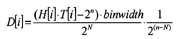 iii) daß die Abweichungen der Segmente von der idealen Umsetzercharakteristik (Dev[k]) berechnet werden durch:

- Selbstkalibrierungsmethode nach Anspruch 1, dadurch gekennzeichnet, daß die benötigte Anzahl an Stichproben für das Histogramm folgendermaßen bestimmt wird:

- Selbstkalibrierungsmethode nach Anspruch 1, dadurch gekennzeichnet, daß die Kalibrierung bei maximaler Umsetzer-Rate erfolgt.
- Analog-Digitalumsetzer Architektur um die Selbstkalibrierungsmethode nach Anspruch 1 auszuführen, bestehend aus:a) einer WGN generierenden Schaltung;b) einer ROM Tabelle (N1 bis N4);c) 2 Registerbänken (C1 bis C4 und Reg 1 bis Reg. 4);d) 2 Addierern und 2 zusätzliche Registern, jeweils eines zum Speichern des Offsets (OFF) und zur Einstellung der Standardabweichung (σ) des WGN Generators.
- ADU Architektur nach Anspruch 4, dadurch gekennzeichnet, daß die ROM Tabelle eine "binwidth " = 1 verwendet und die zusammen mit der WGN generierenden Schaltung und dem ADU am Chip integriert wird, um einen Selbsttest (built-in self-test BIST) für ADU Nichtlinearitäten durchzuführen.
Priority Applications (3)
| Application Number | Priority Date | Filing Date | Title |
|---|---|---|---|
| DE60307232T DE60307232D1 (de) | 2003-03-20 | 2003-03-20 | Techniken zur Selbstkalibrierung im Digitalbereich und für den eingebauten Selbsttest von integrierten Hochgeschwindigkeits-A/D-Wandlern mit Hilfe von weissen Gauss-Geräuschen |
| EP03398002A EP1473836B1 (de) | 2003-03-20 | 2003-03-20 | Techniken zur Selbstkalibrierung im Digitalbereich und für den eingebauten Selbsttest von integrierten Hochgeschwindigkeits-A/D-Wandlern mit Hilfe von weissen Gauss-Geräuschen |
| AT03398002T ATE335306T1 (de) | 2003-03-20 | 2003-03-20 | Techniken zur selbstkalibrierung im digitalbereich und für den eingebauten selbsttest von integrierten hochgeschwindigkeits-a/d- wandlern mit hilfe von weissen gauss-geräuschen |
Applications Claiming Priority (1)
| Application Number | Priority Date | Filing Date | Title |
|---|---|---|---|
| EP03398002A EP1473836B1 (de) | 2003-03-20 | 2003-03-20 | Techniken zur Selbstkalibrierung im Digitalbereich und für den eingebauten Selbsttest von integrierten Hochgeschwindigkeits-A/D-Wandlern mit Hilfe von weissen Gauss-Geräuschen |
Publications (2)
| Publication Number | Publication Date |
|---|---|
| EP1473836A1 EP1473836A1 (de) | 2004-11-03 |
| EP1473836B1 true EP1473836B1 (de) | 2006-08-02 |
Family
ID=32982005
Family Applications (1)
| Application Number | Title | Priority Date | Filing Date |
|---|---|---|---|
| EP03398002A Expired - Lifetime EP1473836B1 (de) | 2003-03-20 | 2003-03-20 | Techniken zur Selbstkalibrierung im Digitalbereich und für den eingebauten Selbsttest von integrierten Hochgeschwindigkeits-A/D-Wandlern mit Hilfe von weissen Gauss-Geräuschen |
Country Status (3)
| Country | Link |
|---|---|
| EP (1) | EP1473836B1 (de) |
| AT (1) | ATE335306T1 (de) |
| DE (1) | DE60307232D1 (de) |
Cited By (1)
| Publication number | Priority date | Publication date | Assignee | Title |
|---|---|---|---|---|
| US9041569B2 (en) | 2013-06-28 | 2015-05-26 | Silicon Laboratories Inc. | Method and apparatus for calibration of successive approximation register analog-to-digital converters |
Families Citing this family (7)
| Publication number | Priority date | Publication date | Assignee | Title |
|---|---|---|---|---|
| JP5189828B2 (ja) * | 2007-11-20 | 2013-04-24 | 株式会社日立製作所 | アナログデジタル変換器チップおよびそれを用いたrf−icチップ |
| US9240798B2 (en) * | 2014-02-28 | 2016-01-19 | Texas Instruments Incorporated | On-chip analog-to-digital converter (ADC) linearity text for embedded devices |
| US9256505B2 (en) | 2014-03-17 | 2016-02-09 | Avago Technologies General Ip (Singapore) Pte. Ltd. | Data transformations to improve ROM yield and programming time |
| DE102017121910B4 (de) | 2017-02-13 | 2021-07-29 | Elmos Semiconductor Se | Ressourceneffizientes Verfahren zur Bewertung der Funktionstüchtigkeit eines Analog-zu-Digital-Wandlers |
| DE102017121909B4 (de) | 2017-09-21 | 2021-07-29 | Elmos Semiconductor Se | Ressourceneffizientes Verfahren zur Bewertung der Funktionstüchtigkeit eines Analog-zu-Digital-Wandlers |
| WO2021072598A1 (zh) * | 2019-10-14 | 2021-04-22 | 深圳市汇顶科技股份有限公司 | 一种数字校准方法、装置及真随机数发生器电路 |
| CN113872598B (zh) * | 2021-08-27 | 2024-11-05 | 西安电子科技大学 | 基于直方图统计的流水线adc后台数字校准方法及装置 |
Family Cites Families (1)
| Publication number | Priority date | Publication date | Assignee | Title |
|---|---|---|---|---|
| SE516157C2 (sv) * | 1999-05-28 | 2001-11-26 | Ericsson Telefon Ab L M | Rättning av statiska fel i en AD-omvandlare |
-
2003
- 2003-03-20 EP EP03398002A patent/EP1473836B1/de not_active Expired - Lifetime
- 2003-03-20 AT AT03398002T patent/ATE335306T1/de not_active IP Right Cessation
- 2003-03-20 DE DE60307232T patent/DE60307232D1/de not_active Expired - Lifetime
Cited By (1)
| Publication number | Priority date | Publication date | Assignee | Title |
|---|---|---|---|---|
| US9041569B2 (en) | 2013-06-28 | 2015-05-26 | Silicon Laboratories Inc. | Method and apparatus for calibration of successive approximation register analog-to-digital converters |
Also Published As
| Publication number | Publication date |
|---|---|
| ATE335306T1 (de) | 2006-08-15 |
| DE60307232D1 (de) | 2006-09-14 |
| EP1473836A1 (de) | 2004-11-03 |
Similar Documents
| Publication | Publication Date | Title |
|---|---|---|
| US7187310B2 (en) | Circuit calibration using voltage injection | |
| US6563445B1 (en) | Self-calibration methods and structures for pipelined analog-to-digital converters | |
| US10840934B2 (en) | Methods and apparatus for a successive approximation register analog-to-digital converter | |
| CN106888018B (zh) | Dac时序失配误差的数字测量 | |
| CN106888020B (zh) | Dac开关失配误差的数字测量 | |
| CN113114247B (zh) | 基于比较时间探测器的流水线adc级间增益校准方法 | |
| US20090085785A1 (en) | Digital-to-analog converter calibration for multi-bit analog-to-digital converters | |
| US5926123A (en) | Self calibration circuitry and algorithm for multipass analog to digital converter interstage gain correction | |
| CN118659783B (zh) | 一种应用于流水线逐次逼近型adc的校准方法及电路 | |
| US20100073207A1 (en) | Delta-Sigma Analog-to-Digital Converters and Methods to Calibrate Delta-Sigma Analog-to-Digital Converters | |
| EP1473836B1 (de) | Techniken zur Selbstkalibrierung im Digitalbereich und für den eingebauten Selbsttest von integrierten Hochgeschwindigkeits-A/D-Wandlern mit Hilfe von weissen Gauss-Geräuschen | |
| Chang et al. | Radix-based digital calibration techniques for multi-stage recycling pipelined ADCs | |
| US10763886B1 (en) | Dithering and calibration technique in multi-stage ADC | |
| US8223049B2 (en) | Charge injection mechanism for analog-to-digital converters | |
| El-Sankary et al. | A background calibration technique for multibit/stage pipelined and time-interleaved ADCs | |
| Goes et al. | Digital-domain self-calibration technique for video-rate pipeline A/D converters using Gaussian white noise | |
| Jin et al. | A digital self-calibration algorithm for ADCs based on histogram test using low-linearity input signals | |
| KR101590480B1 (ko) | 파이프라인 adc | |
| Goes et al. | A CMOS 4-bit MDAC with self-calibrated 14-bit linearity for high-resolution pipelined A/D converters | |
| Chen | A 16b 5MSPS two-stage pipeline ADC with self-calibrated technology | |
| Rombouts et al. | Comments on" Interstage gain-proration technique for digital-domain multistep ADC calibration" | |
| Unterweissacher et al. | Efficient digital self-calibration of video-rate pipeline ADCs using white Gaussian noise | |
| KR100190531B1 (ko) | 아날로그-디지탈 변환장치의 다중 디지탈-아날로그 변환회로 | |
| Ortigueira et al. | Efficient digital self-calibration of video-rate pipeline ADCs using white gaussian noise | |
| Figueiredo et al. | New simple digital self-calibration technique for pipeline ADCs using the internal thermal noise |
Legal Events
| Date | Code | Title | Description |
|---|---|---|---|
| PUAI | Public reference made under article 153(3) epc to a published international application that has entered the european phase |
Free format text: ORIGINAL CODE: 0009012 |
|
| AK | Designated contracting states |
Kind code of ref document: A1 Designated state(s): AT BE BG CH CY CZ DE DK EE ES FI FR GB GR HU IE IT LI LU MC NL PT RO SE SI SK TR |
|
| AX | Request for extension of the european patent |
Extension state: AL LT LV MK |
|
| 17P | Request for examination filed |
Effective date: 20050414 |
|
| AKX | Designation fees paid |
Designated state(s): AT BE BG CH CY CZ DE DK EE ES FI FR GB GR HU IE IT LI LU MC NL PT RO SE SI SK TR |
|
| GRAP | Despatch of communication of intention to grant a patent |
Free format text: ORIGINAL CODE: EPIDOSNIGR1 |
|
| GRAC | Information related to communication of intention to grant a patent modified |
Free format text: ORIGINAL CODE: EPIDOSCIGR1 |
|
| GRAS | Grant fee paid |
Free format text: ORIGINAL CODE: EPIDOSNIGR3 |
|
| RAP1 | Party data changed (applicant data changed or rights of an application transferred) |
Owner name: ACACIA SEMICONDUCTOR, LDA. |
|
| GRAA | (expected) grant |
Free format text: ORIGINAL CODE: 0009210 |
|
| AK | Designated contracting states |
Kind code of ref document: B1 Designated state(s): AT BE BG CH CY CZ DE DK EE ES FI FR GB GR HU IE IT LI LU MC NL PT RO SE SI SK TR |
|
| PG25 | Lapsed in a contracting state [announced via postgrant information from national office to epo] |
Ref country code: IT Free format text: LAPSE BECAUSE OF FAILURE TO SUBMIT A TRANSLATION OF THE DESCRIPTION OR TO PAY THE FEE WITHIN THE PRESCRIBED TIME-LIMIT;WARNING: LAPSES OF ITALIAN PATENTS WITH EFFECTIVE DATE BEFORE 2007 MAY HAVE OCCURRED AT ANY TIME BEFORE 2007. THE CORRECT EFFECTIVE DATE MAY BE DIFFERENT FROM THE ONE RECORDED. Effective date: 20060802 Ref country code: LI Free format text: LAPSE BECAUSE OF FAILURE TO SUBMIT A TRANSLATION OF THE DESCRIPTION OR TO PAY THE FEE WITHIN THE PRESCRIBED TIME-LIMIT Effective date: 20060802 Ref country code: CZ Free format text: LAPSE BECAUSE OF FAILURE TO SUBMIT A TRANSLATION OF THE DESCRIPTION OR TO PAY THE FEE WITHIN THE PRESCRIBED TIME-LIMIT Effective date: 20060802 Ref country code: FI Free format text: LAPSE BECAUSE OF FAILURE TO SUBMIT A TRANSLATION OF THE DESCRIPTION OR TO PAY THE FEE WITHIN THE PRESCRIBED TIME-LIMIT Effective date: 20060802 Ref country code: SI Free format text: LAPSE BECAUSE OF FAILURE TO SUBMIT A TRANSLATION OF THE DESCRIPTION OR TO PAY THE FEE WITHIN THE PRESCRIBED TIME-LIMIT Effective date: 20060802 Ref country code: SK Free format text: LAPSE BECAUSE OF FAILURE TO SUBMIT A TRANSLATION OF THE DESCRIPTION OR TO PAY THE FEE WITHIN THE PRESCRIBED TIME-LIMIT Effective date: 20060802 Ref country code: NL Free format text: LAPSE BECAUSE OF FAILURE TO SUBMIT A TRANSLATION OF THE DESCRIPTION OR TO PAY THE FEE WITHIN THE PRESCRIBED TIME-LIMIT Effective date: 20060802 Ref country code: CH Free format text: LAPSE BECAUSE OF FAILURE TO SUBMIT A TRANSLATION OF THE DESCRIPTION OR TO PAY THE FEE WITHIN THE PRESCRIBED TIME-LIMIT Effective date: 20060802 Ref country code: RO Free format text: LAPSE BECAUSE OF FAILURE TO SUBMIT A TRANSLATION OF THE DESCRIPTION OR TO PAY THE FEE WITHIN THE PRESCRIBED TIME-LIMIT Effective date: 20060802 Ref country code: AT Free format text: LAPSE BECAUSE OF FAILURE TO SUBMIT A TRANSLATION OF THE DESCRIPTION OR TO PAY THE FEE WITHIN THE PRESCRIBED TIME-LIMIT Effective date: 20060802 Ref country code: BE Free format text: LAPSE BECAUSE OF FAILURE TO SUBMIT A TRANSLATION OF THE DESCRIPTION OR TO PAY THE FEE WITHIN THE PRESCRIBED TIME-LIMIT Effective date: 20060802 |
|
| REG | Reference to a national code |
Ref country code: GB Ref legal event code: FG4D |
|
| REG | Reference to a national code |
Ref country code: CH Ref legal event code: EP |
|
| REG | Reference to a national code |
Ref country code: IE Ref legal event code: FG4D |
|
| REF | Corresponds to: |
Ref document number: 60307232 Country of ref document: DE Date of ref document: 20060914 Kind code of ref document: P |
|
| PG25 | Lapsed in a contracting state [announced via postgrant information from national office to epo] |
Ref country code: DK Free format text: LAPSE BECAUSE OF FAILURE TO SUBMIT A TRANSLATION OF THE DESCRIPTION OR TO PAY THE FEE WITHIN THE PRESCRIBED TIME-LIMIT Effective date: 20061102 Ref country code: SE Free format text: LAPSE BECAUSE OF FAILURE TO SUBMIT A TRANSLATION OF THE DESCRIPTION OR TO PAY THE FEE WITHIN THE PRESCRIBED TIME-LIMIT Effective date: 20061102 Ref country code: BG Free format text: LAPSE BECAUSE OF FAILURE TO SUBMIT A TRANSLATION OF THE DESCRIPTION OR TO PAY THE FEE WITHIN THE PRESCRIBED TIME-LIMIT Effective date: 20061102 |
|
| PG25 | Lapsed in a contracting state [announced via postgrant information from national office to epo] |
Ref country code: DE Free format text: LAPSE BECAUSE OF FAILURE TO SUBMIT A TRANSLATION OF THE DESCRIPTION OR TO PAY THE FEE WITHIN THE PRESCRIBED TIME-LIMIT Effective date: 20061103 |
|
| PG25 | Lapsed in a contracting state [announced via postgrant information from national office to epo] |
Ref country code: ES Free format text: LAPSE BECAUSE OF FAILURE TO SUBMIT A TRANSLATION OF THE DESCRIPTION OR TO PAY THE FEE WITHIN THE PRESCRIBED TIME-LIMIT Effective date: 20061113 |
|
| NLV1 | Nl: lapsed or annulled due to failure to fulfill the requirements of art. 29p and 29m of the patents act | ||
| PG25 | Lapsed in a contracting state [announced via postgrant information from national office to epo] |
Ref country code: PT Free format text: LAPSE BECAUSE OF FAILURE TO SUBMIT A TRANSLATION OF THE DESCRIPTION OR TO PAY THE FEE WITHIN THE PRESCRIBED TIME-LIMIT Effective date: 20070102 |
|
| REG | Reference to a national code |
Ref country code: CH Ref legal event code: PL |
|
| EN | Fr: translation not filed | ||
| PLBE | No opposition filed within time limit |
Free format text: ORIGINAL CODE: 0009261 |
|
| STAA | Information on the status of an ep patent application or granted ep patent |
Free format text: STATUS: NO OPPOSITION FILED WITHIN TIME LIMIT |
|
| 26N | No opposition filed |
Effective date: 20070503 |
|
| GBPC | Gb: european patent ceased through non-payment of renewal fee |
Effective date: 20070320 |
|
| PG25 | Lapsed in a contracting state [announced via postgrant information from national office to epo] |
Ref country code: MC Free format text: LAPSE BECAUSE OF NON-PAYMENT OF DUE FEES Effective date: 20070331 Ref country code: IE Free format text: LAPSE BECAUSE OF NON-PAYMENT OF DUE FEES Effective date: 20070320 |
|
| PG25 | Lapsed in a contracting state [announced via postgrant information from national office to epo] |
Ref country code: GB Free format text: LAPSE BECAUSE OF NON-PAYMENT OF DUE FEES Effective date: 20070320 Ref country code: FR Free format text: LAPSE BECAUSE OF FAILURE TO SUBMIT A TRANSLATION OF THE DESCRIPTION OR TO PAY THE FEE WITHIN THE PRESCRIBED TIME-LIMIT Effective date: 20070511 Ref country code: GR Free format text: LAPSE BECAUSE OF FAILURE TO SUBMIT A TRANSLATION OF THE DESCRIPTION OR TO PAY THE FEE WITHIN THE PRESCRIBED TIME-LIMIT Effective date: 20061103 |
|
| PG25 | Lapsed in a contracting state [announced via postgrant information from national office to epo] |
Ref country code: EE Free format text: LAPSE BECAUSE OF FAILURE TO SUBMIT A TRANSLATION OF THE DESCRIPTION OR TO PAY THE FEE WITHIN THE PRESCRIBED TIME-LIMIT Effective date: 20060802 |
|
| PG25 | Lapsed in a contracting state [announced via postgrant information from national office to epo] |
Ref country code: FR Free format text: LAPSE BECAUSE OF FAILURE TO SUBMIT A TRANSLATION OF THE DESCRIPTION OR TO PAY THE FEE WITHIN THE PRESCRIBED TIME-LIMIT Effective date: 20060802 |
|
| PG25 | Lapsed in a contracting state [announced via postgrant information from national office to epo] |
Ref country code: CY Free format text: LAPSE BECAUSE OF FAILURE TO SUBMIT A TRANSLATION OF THE DESCRIPTION OR TO PAY THE FEE WITHIN THE PRESCRIBED TIME-LIMIT Effective date: 20060802 Ref country code: LU Free format text: LAPSE BECAUSE OF NON-PAYMENT OF DUE FEES Effective date: 20070320 |
|
| PG25 | Lapsed in a contracting state [announced via postgrant information from national office to epo] |
Ref country code: TR Free format text: LAPSE BECAUSE OF FAILURE TO SUBMIT A TRANSLATION OF THE DESCRIPTION OR TO PAY THE FEE WITHIN THE PRESCRIBED TIME-LIMIT Effective date: 20060802 Ref country code: HU Free format text: LAPSE BECAUSE OF FAILURE TO SUBMIT A TRANSLATION OF THE DESCRIPTION OR TO PAY THE FEE WITHIN THE PRESCRIBED TIME-LIMIT Effective date: 20070203 |