EP0725534A2 - Verfahren und Vorrichtung zur Bildverarbeitung - Google Patents
Verfahren und Vorrichtung zur Bildverarbeitung Download PDFInfo
- Publication number
- EP0725534A2 EP0725534A2 EP96201066A EP96201066A EP0725534A2 EP 0725534 A2 EP0725534 A2 EP 0725534A2 EP 96201066 A EP96201066 A EP 96201066A EP 96201066 A EP96201066 A EP 96201066A EP 0725534 A2 EP0725534 A2 EP 0725534A2
- Authority
- EP
- European Patent Office
- Prior art keywords
- data
- luminance
- color data
- memory
- image processing
- Prior art date
- Legal status (The legal status is an assumption and is not a legal conclusion. Google has not performed a legal analysis and makes no representation as to the accuracy of the status listed.)
- Granted
Links
Images

Classifications
-
- H—ELECTRICITY
- H04—ELECTRIC COMMUNICATION TECHNIQUE
- H04N—PICTORIAL COMMUNICATION, e.g. TELEVISION
- H04N1/00—Scanning, transmission or reproduction of documents or the like, e.g. facsimile transmission; Details thereof
- H04N1/46—Colour picture communication systems
- H04N1/64—Systems for the transmission or the storage of the colour picture signal; Details therefor, e.g. coding or decoding means therefor
- H04N1/646—Transmitting or storing colour television type signals, e.g. PAL, Lab; Their conversion into additive or subtractive colour signals or vice versa therefor
-
- H—ELECTRICITY
- H04—ELECTRIC COMMUNICATION TECHNIQUE
- H04N—PICTORIAL COMMUNICATION, e.g. TELEVISION
- H04N9/00—Details of colour television systems
- H04N9/79—Processing of colour television signals in connection with recording
- H04N9/87—Regeneration of colour television signals
- H04N9/877—Regeneration of colour television signals by assembling picture element blocks in an intermediate memory
-
- H—ELECTRICITY
- H04—ELECTRIC COMMUNICATION TECHNIQUE
- H04N—PICTORIAL COMMUNICATION, e.g. TELEVISION
- H04N5/00—Details of television systems
- H04N5/76—Television signal recording
- H04N5/78—Television signal recording using magnetic recording
- H04N5/781—Television signal recording using magnetic recording on disks or drums
Definitions
- the present invention relates to an image processing apparatus.
- the magnetic disk called still video floppy disk records a still image by separately frequency modulating the luminance signal and the line-sequential color difference signal and frequency multiplexing these siganls. Consequently, for obtaining an NTSC standard video signal, for example, in a reproducing apparatus, it is necessary to separate the frequency multiplexed FM signal into the luminance component and the color difference component, separately frequency demodulate these components, convert the line-sequential color difference signal into a line-simultaneous signal, and convert these components into said standard video signal.
- An object of the present invention is to provide an image processing apparatus capable of resolving the above-mentioned drawbacks entirely or individually.
- Another object of the present invention is to provide an apparatus capable of precise high-speed processing of image signal with a simple structure.
- Still another object of the present invention is to provide an apparatus capable of high-speed processing of externally given luminance signal and color signal with a simple structure.
- an image processing apparatus comprising:
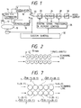
- Fig. 1 is a block diagram of an embodiment of the present invention, wherein shown are a magnetic disk 10 called still video floppy disk; a reproducing head 12; a Y/C separating circuit 14; a demodulation circuit 16 for frequency demodulation of the luminance component of the reproduced signal; a demodulation circuit 18 for frequency demodulation of the line-sequential color difference component of the reproduced signal; a selector switch 20 for selecting the output of the demodulation circuit 16 or 18; an A/D converter 22; a memory 24; a digital signal processing and memory control circuit 26 for controlling the memory 24 and forming an NTSC video signal from the output of the A/D converter 22 and the data stored in the memory 24; a D/A converter 28; a low-pass filter (LPF) 30 for eliminating unnecessary band component; and a system control circuit 32 for controlling the entire apparatus.
- a magnetic disk 10 called still video floppy disk
- a reproducing head 12 for a Y/C separating circuit 14
- a track of the magnetic disk 10, in which a desired image is recorded, is reproduced plural times, and the reproduced signals are subjected to fetching of luminance data and line-sequential color difference data in the memory 24 as will be explained later, and also to conversion into a line-simultaneously signal and into an NTSC signal.
- Fig. 3 is a block diagram of the memory 24, which is composed, in the present embodiment, of two chips of 1 Mbit general-purpose DRAM (for static column mode) of 4 x 256 Kbits. Use of an 8-bit bus in such structure allows to store 8-bit data into the memory 24 with 70 nsec in continuous manner as shown in Fig. 2.
- the refreshing of the memory can be conducted in the image blanking period, and such refreshing method will not be explained further as it is already well known.
- the switch 20 is connected to the contact b in a second field period to supply the output (reproduced line-sequential color difference signal) of the demodulation circuit 18 to the A/D converter 22 for digitizing.
- the digital signal processing and memory control circuit 26 reads, simultaneously with the A/D conversion of the reproduced line-sequential color difference signal, the luminance data from the memory 24 and forms an NTSC signal by addition/subtraction of said luminance data and line-sequential color difference data.
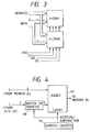
- Fig. 4 shows the structure of a digital NTSC encoder provided for this purpose in the digital signal processing and memory control circuit 26. There are provided a circuit 40 functioning as a buffer in the addition or as an inverter in the subtraction; an adder 42; and an address counter 44.
- the result of addition or subtraction in the circuit shown in Fig. 4 is written in the same address of the memory 24.
- This operation corresponds to a read-modify-write operation in the page mode or the static column mode.
- the read-modify-write cycle cannot be applied to all the luminance data as it takes about 120 - 130 nsec.
- said cycle can be applied to every other pixel, since the color difference singal is line-sequentially recorded.
- the memory 24 contains data as shown in Fig. 5.
- the position of the scanning line and the vertical address of the memory 24 are moved by one in comparison with the processing in the 2nd field period. Consequently, a modulation B-Y is applied to lines subjected to a modulation R-Y in the 2nd field period, and a modulation R-Y is applied to lines subjected to a modulation B-Y in the 2nd field period.
- the memory 24 contains data as shown in Fig. 6.
- the data stored in the memory are simply read in continuous manner and supplied to the D/A converter 28.
- the data from the memory 24 are converted into analog signals by the D/A converter 28; and are subjected to elimination of unnecessary band by the LPF 30, thereby providing an analog NTSC signal. Since all the necessary signals are stored in the memory 24, it is possible to stop the magnetic disk 10 and to interrupt the power supply to the separating circuit 14, demodulation circuits 16, 18 and A/D converter 22.
- the present embodiment allows the use of a low-speed memory, thereby reducing the cost and the power consumption, because the number of bits to be read from the memory per unit time can be reduced in a prolonged reproducing operation.
- the reproduced luminance signal is processed and stored in the memory at first, and said luminance signal is again read from the memory at the succeeding processing of the reproduced color difference signal, but it is also possible to store the reproduced color difference signal into the memory at first.
- Such method can be realised by increasing the read/write rate of the memory.
- the NTSC encoded image signal is stored in the memory, but it is also possible, in the present invention, to store said image signal in another memory.
- the present embodiment allows to reduce the memory capacity, since the reproduced data are converted into the video signal before storage in the memory.
Landscapes
- Engineering & Computer Science (AREA)
- Multimedia (AREA)
- Signal Processing (AREA)
- Television Signal Processing For Recording (AREA)
- Processing Of Color Television Signals (AREA)
Applications Claiming Priority (7)
| Application Number | Priority Date | Filing Date | Title |
|---|---|---|---|
| JP225140/89 | 1989-08-31 | ||
| JP1225140A JP2760078B2 (ja) | 1989-08-31 | 1989-08-31 | データ処理装置 |
| JP22514089 | 1989-08-31 | ||
| JP229682/90 | 1990-08-30 | ||
| JP22968290 | 1990-08-30 | ||
| JP02229682A JP3143463B2 (ja) | 1990-08-30 | 1990-08-30 | 画像処理装置 |
| EP90309590A EP0415798B1 (de) | 1989-08-31 | 1990-08-31 | Bildverarbeitungsvorrichtung |
Related Parent Applications (2)
| Application Number | Title | Priority Date | Filing Date |
|---|---|---|---|
| EP90309590.9 Division | 1990-08-31 | ||
| EP90309590A Division EP0415798B1 (de) | 1989-08-31 | 1990-08-31 | Bildverarbeitungsvorrichtung |
Publications (3)
| Publication Number | Publication Date |
|---|---|
| EP0725534A2 true EP0725534A2 (de) | 1996-08-07 |
| EP0725534A3 EP0725534A3 (de) | 1997-01-22 |
| EP0725534B1 EP0725534B1 (de) | 2001-11-28 |
Family
ID=26526455
Family Applications (2)
| Application Number | Title | Priority Date | Filing Date |
|---|---|---|---|
| EP96201066A Expired - Lifetime EP0725534B1 (de) | 1989-08-31 | 1990-08-31 | Verfahren und Vorrichtung zur Bildverarbeitung |
| EP90309590A Expired - Lifetime EP0415798B1 (de) | 1989-08-31 | 1990-08-31 | Bildverarbeitungsvorrichtung |
Family Applications After (1)
| Application Number | Title | Priority Date | Filing Date |
|---|---|---|---|
| EP90309590A Expired - Lifetime EP0415798B1 (de) | 1989-08-31 | 1990-08-31 | Bildverarbeitungsvorrichtung |
Country Status (3)
| Country | Link |
|---|---|
| US (1) | US5223942A (de) |
| EP (2) | EP0725534B1 (de) |
| DE (2) | DE69029019T2 (de) |
Families Citing this family (7)
| Publication number | Priority date | Publication date | Assignee | Title |
|---|---|---|---|---|
| JPH04245063A (ja) * | 1991-01-31 | 1992-09-01 | Sony Corp | 複製防止用の信号合成回路並びに検出回路 |
| KR970009467B1 (ko) * | 1992-07-21 | 1997-06-13 | 니뽕 빅터 가부시끼 가이샤 | 영상 신호 기록 장치 및 그 재생 장치 |
| DE69319883T2 (de) * | 1992-09-15 | 1998-12-24 | Samsung Electronics Co. Ltd., Suwon, Kyungki | Multiplexsystem für video |
| JPH06189337A (ja) * | 1992-12-21 | 1994-07-08 | Canon Inc | 静止画像信号記録再生装置 |
| JPH07131746A (ja) * | 1993-10-29 | 1995-05-19 | Canon Inc | 電子カメラ |
| US6269215B1 (en) * | 1999-03-02 | 2001-07-31 | Hitachi, Ltd. | Information processing system |
| JP2003037847A (ja) * | 2001-07-26 | 2003-02-07 | Matsushita Electric Ind Co Ltd | 画像処理システム及び撮像装置並びに画像処理装置 |
Family Cites Families (6)
| Publication number | Priority date | Publication date | Assignee | Title |
|---|---|---|---|---|
| US4490749A (en) * | 1980-11-22 | 1984-12-25 | Victor Company Of Japan, Ltd. | Color video signal recording and/or reproducing system |
| JPS57121391A (en) * | 1981-01-19 | 1982-07-28 | Nippon Television Kogyo Kk | Still picture reproducing device |
| JPS58181383A (ja) * | 1982-04-16 | 1983-10-24 | Victor Co Of Japan Ltd | デイジタル信号再生装置 |
| JP2573925B2 (ja) * | 1985-07-16 | 1997-01-22 | 富士写真フイルム株式会社 | 画像ハ−ドコピ−作成装置 |
| US4870509A (en) * | 1986-04-09 | 1989-09-26 | Canon Kabushiki Kaisha | Compact video signal recording and/or reproducing apparatus adapted for external input video signals and variable speed reproduction |
| JPS63294089A (ja) * | 1987-05-27 | 1988-11-30 | Toshiba Corp | 映像記憶装置 |
-
1990
- 1990-08-31 DE DE69029019T patent/DE69029019T2/de not_active Expired - Fee Related
- 1990-08-31 EP EP96201066A patent/EP0725534B1/de not_active Expired - Lifetime
- 1990-08-31 EP EP90309590A patent/EP0415798B1/de not_active Expired - Lifetime
- 1990-08-31 DE DE69033870T patent/DE69033870D1/de not_active Expired - Lifetime
- 1990-08-31 US US07/575,877 patent/US5223942A/en not_active Expired - Lifetime
Also Published As
| Publication number | Publication date |
|---|---|
| EP0725534A3 (de) | 1997-01-22 |
| EP0725534B1 (de) | 2001-11-28 |
| US5223942A (en) | 1993-06-29 |
| DE69029019T2 (de) | 1997-03-06 |
| EP0415798A2 (de) | 1991-03-06 |
| DE69033870D1 (de) | 2002-01-10 |
| DE69029019D1 (de) | 1996-12-05 |
| EP0415798B1 (de) | 1996-10-30 |
| EP0415798A3 (en) | 1992-05-06 |
Similar Documents
| Publication | Publication Date | Title |
|---|---|---|
| US5444483A (en) | Digital electronic camera apparatus for recording still video images and motion video images | |
| EP0725534B1 (de) | Verfahren und Vorrichtung zur Bildverarbeitung | |
| US5341178A (en) | Send-out convertors for a recording/reproducing system | |
| US7295765B1 (en) | Digital image recording and reproducing apparatus having formats corresponding to pixel configurations | |
| US5005080A (en) | Method and apparatus of image processing | |
| US4937668A (en) | Method and apparatus for transmitting video information | |
| JP3350982B2 (ja) | 画像縮小装置 | |
| JP2760078B2 (ja) | データ処理装置 | |
| JP3199220B2 (ja) | 磁気記録再生装置 | |
| JP2603220B2 (ja) | 画像情報伝送方法 | |
| JP2531616B2 (ja) | 画像信号記録装置 | |
| JP2994643B2 (ja) | 画像伝送装置及びその方法 | |
| JPS6462987A (en) | Method of digital picture-recording and regenerating high-definition television signal | |
| JPH04138789A (ja) | 記録装置 | |
| JP3303979B2 (ja) | 画像再生装置 | |
| JPH05167974A (ja) | 映像記録再生装置 | |
| JPS6248887A (ja) | 画像情報信号伝送方法及び装置 | |
| JPS62176386A (ja) | 情報信号伝送システム | |
| JPS62209983A (ja) | 画像情報伝送方法 | |
| EP0559498A1 (de) | Synchronisierungssystem für ein ein hochauflösendes Signal aufzeichnendes Gerät | |
| JPS62149284A (ja) | 画像情報伝送システム | |
| JPH02153682A (ja) | ハイビジヨン画像データのノイズ低減方法 | |
| JPH0955913A (ja) | 記録装置及び記録再生装置 | |
| JPH03178291A (ja) | 映像信号の記録・再生方法 | |
| JPS58119280A (ja) | ビデオ・テ−プ・レコ−ダ編集の制御方式 |
Legal Events
| Date | Code | Title | Description |
|---|---|---|---|
| PUAI | Public reference made under article 153(3) epc to a published international application that has entered the european phase |
Free format text: ORIGINAL CODE: 0009012 |
|
| AC | Divisional application: reference to earlier application |
Ref document number: 415798 Country of ref document: EP |
|
| AK | Designated contracting states |
Kind code of ref document: A2 Designated state(s): DE FR GB |
|
| PUAL | Search report despatched |
Free format text: ORIGINAL CODE: 0009013 |
|
| AK | Designated contracting states |
Kind code of ref document: A3 Designated state(s): DE FR GB |
|
| 17P | Request for examination filed |
Effective date: 19970604 |
|
| 17Q | First examination report despatched |
Effective date: 19990205 |
|
| GRAG | Despatch of communication of intention to grant |
Free format text: ORIGINAL CODE: EPIDOS AGRA |
|
| GRAG | Despatch of communication of intention to grant |
Free format text: ORIGINAL CODE: EPIDOS AGRA |
|
| GRAG | Despatch of communication of intention to grant |
Free format text: ORIGINAL CODE: EPIDOS AGRA |
|
| GRAH | Despatch of communication of intention to grant a patent |
Free format text: ORIGINAL CODE: EPIDOS IGRA |
|
| GRAH | Despatch of communication of intention to grant a patent |
Free format text: ORIGINAL CODE: EPIDOS IGRA |
|
| GRAA | (expected) grant |
Free format text: ORIGINAL CODE: 0009210 |
|
| AC | Divisional application: reference to earlier application |
Ref document number: 415798 Country of ref document: EP |
|
| AK | Designated contracting states |
Kind code of ref document: B1 Designated state(s): DE FR GB |
|
| PG25 | Lapsed in a contracting state [announced via postgrant information from national office to epo] |
Ref country code: FR Free format text: LAPSE BECAUSE OF FAILURE TO SUBMIT A TRANSLATION OF THE DESCRIPTION OR TO PAY THE FEE WITHIN THE PRESCRIBED TIME-LIMIT Effective date: 20011128 |
|
| REG | Reference to a national code |
Ref country code: GB Ref legal event code: IF02 |
|
| REF | Corresponds to: |
Ref document number: 69033870 Country of ref document: DE Date of ref document: 20020110 |
|
| PG25 | Lapsed in a contracting state [announced via postgrant information from national office to epo] |
Ref country code: DE Free format text: LAPSE BECAUSE OF FAILURE TO SUBMIT A TRANSLATION OF THE DESCRIPTION OR TO PAY THE FEE WITHIN THE PRESCRIBED TIME-LIMIT Effective date: 20020301 |
|
| EN | Fr: translation not filed | ||
| PLBE | No opposition filed within time limit |
Free format text: ORIGINAL CODE: 0009261 |
|
| STAA | Information on the status of an ep patent application or granted ep patent |
Free format text: STATUS: NO OPPOSITION FILED WITHIN TIME LIMIT |
|
| 26N | No opposition filed | ||
| PGFP | Annual fee paid to national office [announced via postgrant information from national office to epo] |
Ref country code: GB Payment date: 20040817 Year of fee payment: 15 |
|
| PG25 | Lapsed in a contracting state [announced via postgrant information from national office to epo] |
Ref country code: GB Free format text: LAPSE BECAUSE OF NON-PAYMENT OF DUE FEES Effective date: 20050831 |
|
| GBPC | Gb: european patent ceased through non-payment of renewal fee |
Effective date: 20050831 |