EP0724293A2 - Gatekontaktstruktur eines Leistung-MOS-Transistors - Google Patents
Gatekontaktstruktur eines Leistung-MOS-Transistors Download PDFInfo
- Publication number
- EP0724293A2 EP0724293A2 EP96101056A EP96101056A EP0724293A2 EP 0724293 A2 EP0724293 A2 EP 0724293A2 EP 96101056 A EP96101056 A EP 96101056A EP 96101056 A EP96101056 A EP 96101056A EP 0724293 A2 EP0724293 A2 EP 0724293A2
- Authority
- EP
- European Patent Office
- Prior art keywords
- mos transistor
- gate
- surrounding
- gates
- transistor according
- Prior art date
- Legal status (The legal status is an assumption and is not a legal conclusion. Google has not performed a legal analysis and makes no representation as to the accuracy of the status listed.)
- Withdrawn
Links
Images


Classifications
-
- H—ELECTRICITY
- H10—SEMICONDUCTOR DEVICES; ELECTRIC SOLID-STATE DEVICES NOT OTHERWISE PROVIDED FOR
- H10D—INORGANIC ELECTRIC SEMICONDUCTOR DEVICES
- H10D62/00—Semiconductor bodies, or regions thereof, of devices having potential barriers
- H10D62/10—Shapes, relative sizes or dispositions of the regions of the semiconductor bodies; Shapes of the semiconductor bodies
- H10D62/124—Shapes, relative sizes or dispositions of the regions of semiconductor bodies or of junctions between the regions
- H10D62/126—Top-view geometrical layouts of the regions or the junctions
-
- H—ELECTRICITY
- H10—SEMICONDUCTOR DEVICES; ELECTRIC SOLID-STATE DEVICES NOT OTHERWISE PROVIDED FOR
- H10D—INORGANIC ELECTRIC SEMICONDUCTOR DEVICES
- H10D64/00—Electrodes of devices having potential barriers
- H10D64/20—Electrodes characterised by their shapes, relative sizes or dispositions
- H10D64/27—Electrodes not carrying the current to be rectified, amplified, oscillated or switched, e.g. gates
- H10D64/311—Gate electrodes for field-effect devices
-
- H—ELECTRICITY
- H10—SEMICONDUCTOR DEVICES; ELECTRIC SOLID-STATE DEVICES NOT OTHERWISE PROVIDED FOR
- H10D—INORGANIC ELECTRIC SEMICONDUCTOR DEVICES
- H10D64/00—Electrodes of devices having potential barriers
- H10D64/20—Electrodes characterised by their shapes, relative sizes or dispositions
- H10D64/23—Electrodes carrying the current to be rectified, amplified, oscillated or switched, e.g. sources, drains, anodes or cathodes
- H10D64/251—Source or drain electrodes for field-effect devices
- H10D64/257—Source or drain electrodes for field-effect devices for lateral devices wherein the source or drain electrodes are characterised by top-view geometrical layouts, e.g. interdigitated, semi-circular, annular or L-shaped electrodes
-
- H—ELECTRICITY
- H10—SEMICONDUCTOR DEVICES; ELECTRIC SOLID-STATE DEVICES NOT OTHERWISE PROVIDED FOR
- H10D—INORGANIC ELECTRIC SEMICONDUCTOR DEVICES
- H10D64/00—Electrodes of devices having potential barriers
- H10D64/20—Electrodes characterised by their shapes, relative sizes or dispositions
- H10D64/27—Electrodes not carrying the current to be rectified, amplified, oscillated or switched, e.g. gates
- H10D64/311—Gate electrodes for field-effect devices
- H10D64/411—Gate electrodes for field-effect devices for FETs
- H10D64/511—Gate electrodes for field-effect devices for FETs for IGFETs
- H10D64/517—Gate electrodes for field-effect devices for FETs for IGFETs characterised by the conducting layers
- H10D64/519—Gate electrodes for field-effect devices for FETs for IGFETs characterised by the conducting layers characterised by their top-view geometrical layouts
-
- H—ELECTRICITY
- H10—SEMICONDUCTOR DEVICES; ELECTRIC SOLID-STATE DEVICES NOT OTHERWISE PROVIDED FOR
- H10D—INORGANIC ELECTRIC SEMICONDUCTOR DEVICES
- H10D64/00—Electrodes of devices having potential barriers
- H10D64/60—Electrodes characterised by their materials
- H10D64/66—Electrodes having a conductor capacitively coupled to a semiconductor by an insulator, e.g. MIS electrodes
- H10D64/68—Electrodes having a conductor capacitively coupled to a semiconductor by an insulator, e.g. MIS electrodes characterised by the insulator, e.g. by the gate insulator
- H10D64/691—Electrodes having a conductor capacitively coupled to a semiconductor by an insulator, e.g. MIS electrodes characterised by the insulator, e.g. by the gate insulator comprising metallic compounds, e.g. metal oxides or metal silicates
-
- H—ELECTRICITY
- H10—SEMICONDUCTOR DEVICES; ELECTRIC SOLID-STATE DEVICES NOT OTHERWISE PROVIDED FOR
- H10D—INORGANIC ELECTRIC SEMICONDUCTOR DEVICES
- H10D84/00—Integrated devices formed in or on semiconductor substrates that comprise only semiconducting layers, e.g. on Si wafers or on GaAs-on-Si wafers
- H10D84/01—Manufacture or treatment
- H10D84/0123—Integrating together multiple components covered by H10D12/00 or H10D30/00, e.g. integrating multiple IGBTs
- H10D84/0126—Integrating together multiple components covered by H10D12/00 or H10D30/00, e.g. integrating multiple IGBTs the components including insulated gates, e.g. IGFETs
- H10D84/0135—Manufacturing their gate conductors
-
- H10P14/416—
-
- H10W20/484—
-
- H—ELECTRICITY
- H10—SEMICONDUCTOR DEVICES; ELECTRIC SOLID-STATE DEVICES NOT OTHERWISE PROVIDED FOR
- H10D—INORGANIC ELECTRIC SEMICONDUCTOR DEVICES
- H10D64/00—Electrodes of devices having potential barriers
- H10D64/20—Electrodes characterised by their shapes, relative sizes or dispositions
- H10D64/23—Electrodes carrying the current to be rectified, amplified, oscillated or switched, e.g. sources, drains, anodes or cathodes
- H10D64/251—Source or drain electrodes for field-effect devices
- H10D64/256—Source or drain electrodes for field-effect devices for lateral devices wherein the source or drain electrodes are recessed in semiconductor bodies
Definitions
- the present invention relates to a MOS field effect transistor (MOS-FET).
- MOS-FET MOS field effect transistor
- the present invention relates to a power transistor supplying a large current to an output terminal thereof.
- the present invention furthermore relates to a transistor for driving a relatively heavy load, and more specifically, to a transistor for driving an inductive load including motors while switching.
- Fig. 1 shows an example where a plurality of MOS transistor blocks are formed on a semiconductor chip, and connected together to form a single power integrated circuit (IC).
- IC integrated circuit
- MOS transistors Q 1 -Q n which are transistor blocks, are connected in parallel to each other, wherein the gates of the transistors, which are connected to each other, the drains thereof, which are connected to each other, and the sources thereof, which are connected to each other, are led to a terminal G, a terminal D, and a terminal C, respectively.
- the power IC 1 so configured has a power supply connected to the terminal D and a motor 2 connected to the terminal S; when an input signal having a level for turning on the transistors Q 1 -Q n is supplied to the terminal G, each transistor is turned on, so the power supply current from the terminal D is fed through each transistor to the terminal S. The current fed to the terminal S is then supplied as a motor drive current to the motor 2.
- connection between the transistor blocks in this power IC 1 may be generally explained in a semiconductor chip by way of the schematic diagram as shown in Fig. 2
- a source s and a drain d are formed on a semiconductor substrate 11, and a gate g, which comprises polysilicon, is further laminated thereon via a silicon oxide film and so on. If the so-called single-layer aluminum wiring process is used for the entire connection throughout the transistor blocks formed based on the semiconductor substrate 11, aluminum is used for wiring between the sources and between the drains in two adjacent transistor blocks as shown, such as Q m and Q m+1 , whereas the same (or common) polysilicon as that of the gates is used for wiring between the gates.
- MOS transistor that equalizes and accelerates propagation delay times of an input signal from an input terminal to the respective gates.
- the MOS transistor according to the present invention includes a plurality of transistor blocks formed by sources which are connected to each other by a first electric conductive layer, drains which are connected to each other by a second electric conductive layer, and gates made of a continuous semiconductor layer, the improvement comprising a third electric conductive layer which is connected to a gate terminal and laminated on said gates.
- the conductive layer laminated on the gates formed of a continuous semiconductor layer propagates an input signal to the gate of each transistor block with relatively little delay.
- Fig. 1 is a circuit diagram depicting a prior art power IC where a plurality of MOS transistor blocks are connected together.
- Fig. 2 is a schematic diagram depicting a wiring configuration for each electrode of the power IC of Fig. 1.
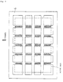
- Fig. 3 is a plan perspective view depicting the structure of a MOS transistor according to one (first) embodiment of the present invention.
- Fig. 4 is a cross-sectional view along X-X of the MOS transistor of Fig. 3.
- Fig. 5 is a cross-sectional view along Y-Y of the MOS transistor of Fig. 3.
- Fig. 6 is a partial perspective view depicting the arrangement of the drain and source in the MOS transistor of Fig. 3.
- Fig. 7 is a partial perspective view depicting the shape of the gate in the MOS transistor of Fig. 3.
- Fig. 8 is a partial perspective view depicting the channel formed in the MOS transistor of Fig. 3.
- Fig. 9 is a plan perspective view depicting the structure of a MOS transistor according to another (second) embodiment of the present invention.
- Fig. 10 is a cross-sectional view along X-X of the MOS transistor of Fig. 9.
- Fig. 11 is a cross-sectional view along Y-Y of the MOS transistor of Fig. 9.
- Fig. 12 is a partial perspective view depicting the arrangement of the drain and source in the MOS transistor of Fig. 9.
- Fig. 13 is a partial perspective view depicting the shape of the gate in the MOS transistor of Fig. 9.
- Fig. 14 is a partial perspective view depicting the channel formed in the MOS transistor of Fig. 9.
- Fig. 15 is a schematic diagram for explaining a method for equalizing the delay time of a gate input signal (where neither the first nor second embodiment is applicable).
- Fig. 16 is a schematic diagram for explaining a method for equalizing the delay time of a gate input signal (where the first embodiment is applicable).
- Fig. 17 is a schematic diagram for explaining a method for equalizing the delay time of a gate input signal (where the second embodiment is applicable).
- Fig. 18 is a schematic diagram for explaining a method for equalizing the delay time of a gate input signal (where the second embodiment is modified).
- Fig. 19 is a plan view for explaining why polysilicon is used for each gate of each transistor block, depicting the structure of a metal gate transistor and a polysilicon gate transistor.
- Fig. 3 is a plan perspective view depicting the structure of a MOS transistor according to one embodiment of the present invention
- Fig. 4 is a cross-sectional view along X-X of Fig. 3
- Fig. 5 is a cross-sectional view along Y-Y of Fig. 5.
- Figs. 6-8 are partial perspective views of Fig. 3.
- a plurality of drains and corresponding sources formed by so-called diffusion are disposed in a semiconductor substrate 3 (which is represented by a thick solid line) formed of p-type polysilicon.
- the drain and source regions extending in the vertical direction are arranged alternatively in the horizontal direction on the semiconductor chip 3, as shown in Fig. 6.
- the drains 4 11 - 4 41 , 4 12 - 4 42 , and 4 13 - 4 43 are arranged vertically in the first, second, and third drain regions, respectively.
- the sources 5 11 - 5 41 , 5 12 - 5 42 , and 5 13 - 5 43 are arranged vertically in the first, second, and third source regions, respectively.
- a gate 6 (which is represented by a thin solid line) formed of, for example, polysilicon, is laminated through an oxide film 7, such as SiO 2 , between the sources, between the drains, and between the source and drain. That is, as shown in Fig. 7, the gate 6 takes a grid-like shape, such that it covers gaps between the drains and sources, as viewed from the front. In other words, the gate 6 has vertically extending portions 6 11 - 6 15 and horizontally extending portions 6 21 - 6 23 along a principal plane of the semiconductor substrate 3.
- the sources 4 11 - 4 43 and drains 5 11 - 5 43 are formed in regions (first through third drain and source regions) separated by the vertically extending portions 6 11 - 6 15 of the gate 6, which are laminated through the oxide film 7 between the sources and drains. Furthermore, the gate 6 has a surrounding portion 6 30 that couples the vertically and horizontally extending portions to each other.
- channels are formed on the semiconductor substrate 3. Such channels are also represented by reference symbol "CH” in Fig. 5.
- CH reference symbol
- 20 channels are formed on the semiconductor substrate, indicating that 20 transistor blocks are formed.
- the drains and sources are connected by one-direction connecting portions (layers) 8 1 - 8 6 , which are conductors, such as aluminum, as denoted by a thin alternate long and short dash line, for each region. More specifically, the drains 4 11 - 4 41 , sources 5 11 - 5 41 , drains 4 12 - 4 42 , sources 5 12 - 5 42 , drain 4 13 - 4 43 , and sources 5 13 - 5 43 are connected to each other by the connecting portion 8 2 , 8 3 , 8 4 , 8 5 , and 8 6 , respectively.
- a contact hole, which is a node between the one-direction connecting portion and the drain and source is represented by mark " ⁇ " in Fig. 3.
- an other-direction connecting portion 9 for commonly connecting the one-direction connecting portions 8 1 , 8 3 , and 8 5 connected to the drains
- an other-direction connecting portion 10 for commonly connecting the one-direction connecting portions 8 2 , 8 4 , and 8 6 connected to the sources.
- These other-direction connecting portions which are represented by a thick alternate long and short dash line in the figures, are also formed of a conductor such as aluminum. Nodes between the other-direction connecting portions 9 and 10 and the one-direction connecting portions, i.e., so-called "via holes", are denoted by " ⁇ " overlapped by "X".
- a conductor 11 such as aluminum, which is denoted by a thin alternate long and two short dashes line, is laminated in contact therewith, and one end of the conductor 11 and the gate terminal of the overall MOS transistor are connected together.
- a node between the conductor 11 and gate 6, i.e., a contact hole, is also represented by " ⁇ " in Fig. 3.
- an insulating film 12 is formed around the contact hole of the conductor 11.
- the signal propagation time for the gate 6 is reduced by the conductor 11 disposed on the gate 6.
- the propagation of the input signal from a terminal Gin located at one corner of the rectangular conductor 11 to a point P on the gate is achieved fast enough to practically ignore the resistance because the conductor 11 extends to reach around the point P, so that the transistor blocks containing the point P provide quite good response to the input signal.
- the conductor 11 that extends around the point P is absent, only the propagation through polysilicon of the gate 6 is effective, so such responsiveness as offered by the present invention could not be achieved.
- the MOS transistor of the present embodiment can be fabricated with reasonable efficiency, by fabricating the conductors 8 1 - 8 6 for connecting the drains and source in one direction, and the gate-laminated conductor 11 at a single-layer aluminum wiring process step, and fabricating the conductors 9 and 10 for connecting the drains and sources in the other direction at a second-layer aluminum wiring process step.
- all the conductors may be formed at a single-layer wiring process step, depending on how well the layout is done on the semiconductor substrate. This may increase the entire area of the semiconductor chip required for the layout or require more precise micro-machining technology, as compared to a two-layer aluminum wiring process.
- the structure has been described where the conductor 11 is laminated only around the surrounding portion 6 30 of the gate 6, although the conductor may also be laminated near some of the vertically and horizontally extending portions of the grid-shaped gate.
- Fig. 9 is a plan perspective view depicting the structure of a MOS transistor according to another embodiment of the present invention.
- Fig. 10 is a cross-sectional view along X-X of Fig. 9; and
- Fig. 11 is a cross-sectional view along Y-Y of Fig. 9.
- Figs. 12-14 are partial perspective views of Fig. 9.
- the gate 6 has guides 6 41 and 6 42 for extending the conductor 11 to near the center of the gate plane thereof, as shown in Fig. 13.
- the guides 6 41 and 6 42 serve as the source side and drain side, respectively.
- two sources and two drains are not formed under these guides.
- twelve channels are formed as shown in Fig. 14, so the number of transistor blocks used is reduced by 4, as compared to that shown in Fig. 8.
- the conductor 11 extends from the surrounding portion 6 30 to the horizontally extending portion 6 22 , as can be seen from Fig. 9.
- This allows the input signal from the terminal Gin to be propagated, with relatively little delay, to the gate near the conductor extending inward, so that the transistor blocks in which the channels are formed by that gate offer better response than the above-described embodiment.
- the present embodiment allows the input signal to be propagated to the gate with a relatively uniform delay time over the entire transistor blocks formed on the semiconductor substrate 3. Additionally, it advantageously eliminates the need for changing the area of the entire semiconductor chip.
- the structure of this embodiment is equivalent or equal to the structure where the conductor 11 is laminated on some of the vertically extending portions of the grid-shaped gate 6.
- the conductor 11 has been described as being extended vertically inward from the surrounding portion, it may be extended horizontally inward.
- Fig. 15 is a schematic diagram depicting the grid-shaped polysilicon gate 6 as one plane, where the aspect ratio (vertical to horizontal ratio) of the gate is 1:3 and neither the first nor second embodiment is applicable.
- FIG. 16 A schematic diagram similar to Fig. 15 is shown in Fig. 16, where the above first embodiment is applicable.
- FIG. 17 a schematic diagram similar to Figs. 15 and 16 is shown in Fig. 17, where the above second embodiment is applicable.
- the conductor 11 is laminated on the surrounding portions of the gate 6, and leads from the conductor are extended inward to the gate 6 at five locations (indicated by ⁇ ). That is, the conductor 11 is connected to the gate 6 not only in the surrounding portions but also at such locations.
- the distance over which the gate signal input at G IN1 is propagated to the location where the largest delay is involved (denoted by a alternate long and short dash line) is given by:
- the delay time in the case of Fig. 16 is increased by a factor of 0.15 as compared to Equation (1) for Fig. 15, and by a factor of 0.08 in the case of Fig. 17.
- the delay time in the case of Fig. 16 is increased by a factor of 0.28 as compared to Equation (2) for Fig. 15, and by a factor of 0.14 in the case of Fig. 17.
- any gate delay time can be set. For example, as compared to a switching time of 200 msec for the MOS transistor configured as in Fig. 15, this method permits a switching time of 20 nsec to be set accurately.
- the present invention is not limited to such a pattern of conductive layer that laminated on the gate. That is, in the above explanation, it has been described that the conductive layer laminated on the gate is comprised of a conductive surrounding portions extending along the perimeter of the distribution areas (generally denoted by active areas in Figs. 3-14) of the gate, and the method described with reference to Figs. 15-17 preferably equalizes the gate delay time, based on the assumption that the surrounding extending portion is comprised of four sides of a rectangle. However, the conductive surrounding extending portion may be comprised of three sides of a rectangle. Referring to Fig.
- the conductor 11 extends from these three sides along the perimeter of the gate 6, and comprised of a connecting portion for connecting a middle point (denoted by ⁇ ) located at or near the center of the distribution area with the conductive surrounding extending portion.
- a connecting portion assumes a shape of straight line extending vertically from the conductive surrounding extending portion, and connects the middle points distributed at regular intervals of a/2 on the straight line segment (denoted by a dotted line) surrounded by and separated away by an equal distance of a/2 from the conductive surrounding extending portion, with the conductive surrounding extending portion.
- the distance between the middle points is equal to the distance of a/2 between the middle point and the conductive surrounding extending portion.
- the distance between an end of the straight line segment near the remaining one side S where the conductor is absent in the gate surrounding portion and that side S is half the distance a/2 between the middle point and conductive surrounding portion, that is, a/4.
- the delay time can be equalized in a similar manner to that shown in Fig. 17.
- various types of conductor patterns on the gate are possible, and may be designed appropriately according to a desired switching time for the MOS transistor.
- the first reason is that polysilicon may be easily established on a gate-length layout.
- a mask for forming a gate oxide film is required, so that unless some consideration is given to the overlap (OL) between the source and drain regions and the aluminum gate, the overlap may become non-existent due to mask misalignment, resulting in improper operation. In addition, the overlap itself assumes a capacitive load, which causes unstable operation of the transistor block.
- a mask for forming a gate oxide film is not necessary; after the formation of the polysilicon gate, that gate itself may be used as a mask to perform so-called self-aligned ion implantation, thereby forming the source and drain.
- a channel proportional to the length L of the polysilicon gate is formed, and because the capacitive load due to an overlap between the source and drain regions and the polysilicon gate is determined solely by lateral diffusion in the source and drain, thus eliminating the need for consideration given to the overlap.
- the second reason is that polysilicon is suitable for a high-temperature process for forming sources and drains.
- source and drain layers it is necessary to expose source and drain layers to a high temperature of 900-950 degrees Celsius during such a high-temperature process; because aluminum has a melting point of about 400 degrees Celsius, an aluminum gate cannot serve as a self-alignment mask as shown in Fig. 19 (B), so that sources and drains cannot be formed after laminating the aluminum gate. That is, during a high-temperature process where sources and drains are formed at temperatures exceeding the melting point of aluminum, it is necessary to form the sources and drains before lamination of the aluminum gate. In contrast, because polysilicon has a melting point of 1300 degrees Celsius, it can sufficiently withstand such a self-aligned high-temperature process.
- the semiconductor substrate 1 has been described as p-type silicon, it is not limited thereto, but may be of n-type and other semiconductors.
- sources and drains, as wall as conductors, oxide films, and insulating films may be formed of various kinds of material and in various shapes.
- the number of transistor has been shown in the embodiments by way of example only, so it may be, of course, greater or smaller than that number.
- sources and drains have been arranged vertically and horizontally in an orderly fashion, it is not limited thereto, but the present invention may be applicable regardless of the vertical or horizontal direction, if the gates commonly formed (or formed of a continuous semiconductor layer) are disposed between the sources and drains via the gate oxide film (or insulator).
- an input signal to a gate of each transistor block is propagated with relatively little delay by a conductive layer laminated on the gate made of a continuous semiconductor layer, so that the delay times of an input signal to the respective gates can be equalized.
- the delay time of a gate input signal to the transistor block located at the center of the semiconductor chip can be substantially reduced. Additionally, the larger the chip area of the MOS transistor, the better the inherent benefit of the present invention.
- the present invention improves the switching speed associated with the output of a motor drive current having a heavy load of 1A, even when a power IC having a transistor block with a gate width of 1000 ⁇ m or wider is employed.
Landscapes
- Insulated Gate Type Field-Effect Transistor (AREA)
- Metal-Oxide And Bipolar Metal-Oxide Semiconductor Integrated Circuits (AREA)
- Semiconductor Integrated Circuits (AREA)
Applications Claiming Priority (2)
| Application Number | Priority Date | Filing Date | Title |
|---|---|---|---|
| JP7011317A JP2997179B2 (ja) | 1995-01-27 | 1995-01-27 | パワーmosトランジスタ |
| JP11317/95 | 1995-01-27 |
Publications (2)
| Publication Number | Publication Date |
|---|---|
| EP0724293A2 true EP0724293A2 (de) | 1996-07-31 |
| EP0724293A3 EP0724293A3 (de) | 1996-08-14 |
Family
ID=11774652
Family Applications (1)
| Application Number | Title | Priority Date | Filing Date |
|---|---|---|---|
| EP96101056A Withdrawn EP0724293A3 (de) | 1995-01-27 | 1996-01-25 | Gatekontaktstruktur eines Leistung-MOS-Transistors |
Country Status (4)
| Country | Link |
|---|---|
| US (1) | US5693966A (de) |
| EP (1) | EP0724293A3 (de) |
| JP (1) | JP2997179B2 (de) |
| KR (1) | KR100326693B1 (de) |
Cited By (4)
| Publication number | Priority date | Publication date | Assignee | Title |
|---|---|---|---|---|
| EP0766309A3 (de) * | 1995-08-28 | 1998-04-29 | Texas Instruments Incorporated | Feldeffekttransistor mit mehrschichtiger Metallisierung und integrierter Schaltung dafür |
| FR2759493A1 (fr) * | 1997-02-12 | 1998-08-14 | Motorola Semiconducteurs | Dispositif de puissance a semiconducteur |
| EP1391989A1 (de) * | 2001-07-31 | 2004-02-25 | Nokia Corporation | Abstimmschaltung und IGFET |
| DE102016100504A1 (de) * | 2016-01-13 | 2017-07-13 | Infineon Technologies Ag | Transistorbauelement mit segmentierter Kontaktschicht |
Families Citing this family (3)
| Publication number | Priority date | Publication date | Assignee | Title |
|---|---|---|---|---|
| US5977830A (en) * | 1996-12-03 | 1999-11-02 | Lucent Technologies Inc. | Low noise transistor module and amplifier |
| JP3696211B2 (ja) | 2003-02-10 | 2005-09-14 | 株式会社東芝 | パワースイッチング装置 |
| JP4687066B2 (ja) * | 2004-10-25 | 2011-05-25 | 株式会社デンソー | パワーic |
Family Cites Families (8)
| Publication number | Priority date | Publication date | Assignee | Title |
|---|---|---|---|---|
| JP2558931B2 (ja) * | 1990-07-13 | 1996-11-27 | 株式会社東芝 | 半導体装置およびその製造方法 |
| JPH0499378A (ja) * | 1990-08-18 | 1992-03-31 | Nec Corp | 半導体装置 |
| JPH04109677A (ja) * | 1990-08-29 | 1992-04-10 | Seiko Instr Inc | Mosトランジスター |
| US5341014A (en) * | 1992-01-07 | 1994-08-23 | Matsushita Electric Industrial Co., Ltd. | Semiconductor device and a method of fabricating the same |
| EP0623962A1 (de) * | 1993-05-05 | 1994-11-09 | Texas Instruments Deutschland Gmbh | Gate-Electrode eines Leistung-MOS-Feldeffekttransistors |
| US5412239A (en) * | 1993-05-14 | 1995-05-02 | Siliconix Incorporated | Contact geometry for improved lateral MOSFET |
| US5486715A (en) * | 1993-10-15 | 1996-01-23 | Ixys Corporation | High frequency MOS device |
| US5355008A (en) * | 1993-11-19 | 1994-10-11 | Micrel, Inc. | Diamond shaped gate mesh for cellular MOS transistor array |
-
1995
- 1995-01-27 JP JP7011317A patent/JP2997179B2/ja not_active Expired - Fee Related
-
1996
- 1996-01-16 US US08/585,992 patent/US5693966A/en not_active Expired - Lifetime
- 1996-01-24 KR KR1019960001473A patent/KR100326693B1/ko not_active Expired - Fee Related
- 1996-01-25 EP EP96101056A patent/EP0724293A3/de not_active Withdrawn
Non-Patent Citations (1)
| Title |
|---|
| None |
Cited By (8)
| Publication number | Priority date | Publication date | Assignee | Title |
|---|---|---|---|---|
| EP0766309A3 (de) * | 1995-08-28 | 1998-04-29 | Texas Instruments Incorporated | Feldeffekttransistor mit mehrschichtiger Metallisierung und integrierter Schaltung dafür |
| FR2759493A1 (fr) * | 1997-02-12 | 1998-08-14 | Motorola Semiconducteurs | Dispositif de puissance a semiconducteur |
| EP0859414A1 (de) * | 1997-02-12 | 1998-08-19 | Motorola Semiconducteurs S.A. | Halbleiter-Leistungsanordnung |
| US5945730A (en) * | 1997-02-12 | 1999-08-31 | Motorola, Inc. | Semiconductor power device |
| EP1391989A1 (de) * | 2001-07-31 | 2004-02-25 | Nokia Corporation | Abstimmschaltung und IGFET |
| US6992532B2 (en) | 2001-07-31 | 2006-01-31 | Nokia Corporation | IGFET and tuning circuit |
| DE102016100504A1 (de) * | 2016-01-13 | 2017-07-13 | Infineon Technologies Ag | Transistorbauelement mit segmentierter Kontaktschicht |
| DE102016100504B4 (de) | 2016-01-13 | 2021-11-18 | Infineon Technologies Ag | Transistorbauelement mit segmentierter Kontaktschicht |
Also Published As
| Publication number | Publication date |
|---|---|
| US5693966A (en) | 1997-12-02 |
| KR960030442A (ko) | 1996-08-17 |
| KR100326693B1 (ko) | 2002-08-14 |
| EP0724293A3 (de) | 1996-08-14 |
| JP2997179B2 (ja) | 2000-01-11 |
| JPH08204183A (ja) | 1996-08-09 |
Similar Documents
| Publication | Publication Date | Title |
|---|---|---|
| TWI414043B (zh) | 電移適用高效能fet佈局 | |
| US5196373A (en) | Method of making trench conductor and crossunder architecture | |
| JPS6286763A (ja) | 分布電界効果トランジスタ構成体 | |
| KR100273745B1 (ko) | 반도체장치 | |
| US7091554B2 (en) | Semiconductor device | |
| CN1033116C (zh) | 互补金属氧化物半导体集成电路 | |
| US5693966A (en) | Power MOS transistor | |
| US4750026A (en) | C MOS IC and method of making the same | |
| US20250120174A1 (en) | Wiring in diffusion breaks in an integrated circuit | |
| US5057445A (en) | Method of making a high-voltage, low on-resistance igfet | |
| US5055904A (en) | Semiconductor device | |
| JP2867948B2 (ja) | 半導体記憶装置とその製造方法 | |
| HK1008370A (en) | Gate compacting structure of power mos transistor | |
| US11677401B2 (en) | 3D integrated count | |
| US6861705B2 (en) | Driver circuits and methods for manufacturing driver circuits | |
| US6437402B1 (en) | Power MOS transistor | |
| KR100225944B1 (ko) | 가변 드레인 전류형 트랜지스터를 갖는 반도체 장치 | |
| JP2839722B2 (ja) | 集積回路装置 | |
| JPH11135647A (ja) | 半導体装置 | |
| KR20230002969A (ko) | 인접한 특징부들 사이에 전도성 파이프를 형성하는 방법 및 인접한 특징부들 사이에 전도성 파이프를 갖는 집적 조립체 | |
| JP3033372B2 (ja) | 半導体装置 | |
| JP2911345B2 (ja) | 半導体集積回路装置 | |
| JPH0714004B2 (ja) | 半導体装置 | |
| JPH04215473A (ja) | スタティックram | |
| JP3019764B2 (ja) | 半導体集積回路装置およびその回路セルの多段接続構造 |
Legal Events
| Date | Code | Title | Description |
|---|---|---|---|
| PUAI | Public reference made under article 153(3) epc to a published international application that has entered the european phase |
Free format text: ORIGINAL CODE: 0009012 |
|
| PUAL | Search report despatched |
Free format text: ORIGINAL CODE: 0009013 |
|
| AK | Designated contracting states |
Kind code of ref document: A2 Designated state(s): FR GB IT |
|
| AK | Designated contracting states |
Kind code of ref document: A3 Designated state(s): FR GB IT |
|
| 17P | Request for examination filed |
Effective date: 19970214 |
|
| 17Q | First examination report despatched |
Effective date: 19981109 |
|
| STAA | Information on the status of an ep patent application or granted ep patent |
Free format text: STATUS: THE APPLICATION IS DEEMED TO BE WITHDRAWN |
|
| 18D | Application deemed to be withdrawn |
Effective date: 20011218 |
|
| REG | Reference to a national code |
Ref country code: HK Ref legal event code: WD Ref document number: 1008370 Country of ref document: HK |