EP0711447B1 - Programmierbare logische vorrichtung mit einer prüfschaltung zum klassifizieren von schmelzverbindungszuständen als gültig geschlossen, gültig geöffnet oder ungültig - Google Patents
Programmierbare logische vorrichtung mit einer prüfschaltung zum klassifizieren von schmelzverbindungszuständen als gültig geschlossen, gültig geöffnet oder ungültig Download PDFInfo
- Publication number
- EP0711447B1 EP0711447B1 EP95915990A EP95915990A EP0711447B1 EP 0711447 B1 EP0711447 B1 EP 0711447B1 EP 95915990 A EP95915990 A EP 95915990A EP 95915990 A EP95915990 A EP 95915990A EP 0711447 B1 EP0711447 B1 EP 0711447B1
- Authority
- EP
- European Patent Office
- Prior art keywords
- parameter
- current
- link
- value
- circuit
- Prior art date
- Legal status (The legal status is an assumption and is not a legal conclusion. Google has not performed a legal analysis and makes no representation as to the accuracy of the status listed.)
- Expired - Lifetime
Links
- 238000012795 verification Methods 0.000 claims description 33
- 230000004044 response Effects 0.000 claims description 8
- 238000000034 method Methods 0.000 claims description 5
- 238000005259 measurement Methods 0.000 description 11
- 238000012360 testing method Methods 0.000 description 8
- 238000010586 diagram Methods 0.000 description 3
- 238000011990 functional testing Methods 0.000 description 3
- 230000009471 action Effects 0.000 description 2
- 230000003213 activating effect Effects 0.000 description 2
- 238000013459 approach Methods 0.000 description 2
- 238000003491 array Methods 0.000 description 2
- 230000000295 complement effect Effects 0.000 description 2
- 239000004020 conductor Substances 0.000 description 2
- 238000013461 design Methods 0.000 description 2
- 238000005516 engineering process Methods 0.000 description 2
- 230000006870 function Effects 0.000 description 2
- 230000002411 adverse Effects 0.000 description 1
- 230000015572 biosynthetic process Effects 0.000 description 1
- 230000008878 coupling Effects 0.000 description 1
- 238000010168 coupling process Methods 0.000 description 1
- 238000005859 coupling reaction Methods 0.000 description 1
- 230000001419 dependent effect Effects 0.000 description 1
- 230000000694 effects Effects 0.000 description 1
- 239000000463 material Substances 0.000 description 1
- 230000000541 pulsatile effect Effects 0.000 description 1
Images


Classifications
-
- G—PHYSICS
- G11—INFORMATION STORAGE
- G11C—STATIC STORES
- G11C17/00—Read-only memories programmable only once; Semi-permanent stores, e.g. manually-replaceable information cards
- G11C17/14—Read-only memories programmable only once; Semi-permanent stores, e.g. manually-replaceable information cards in which contents are determined by selectively establishing, breaking or modifying connecting links by permanently altering the state of coupling elements, e.g. PROM
- G11C17/16—Read-only memories programmable only once; Semi-permanent stores, e.g. manually-replaceable information cards in which contents are determined by selectively establishing, breaking or modifying connecting links by permanently altering the state of coupling elements, e.g. PROM using electrically-fusible links
-
- G—PHYSICS
- G11—INFORMATION STORAGE
- G11C—STATIC STORES
- G11C29/00—Checking stores for correct operation ; Subsequent repair; Testing stores during standby or offline operation
-
- G—PHYSICS
- G11—INFORMATION STORAGE
- G11C—STATIC STORES
- G11C29/00—Checking stores for correct operation ; Subsequent repair; Testing stores during standby or offline operation
- G11C29/04—Detection or location of defective memory elements, e.g. cell constructio details, timing of test signals
- G11C29/08—Functional testing, e.g. testing during refresh, power-on self testing [POST] or distributed testing
- G11C29/12—Built-in arrangements for testing, e.g. built-in self testing [BIST] or interconnection details
- G11C29/44—Indication or identification of errors, e.g. for repair
Definitions
- the present invention relates to programmable logic devices (PLD's) of a type in which an internal memory of fuse or and-fuse links is programmable via program circuitry to achieve a desired pattern of "open” and "closed” link states which are verifiable via the program circuitry. More specifically, the invention relates to an electronic circuit that comprises a memory array of programmable elements, each element having an electrical property which is describable by a parameter and which is alterable from an unprogrammed condition in response to an application of energy directed to the element.
- the parameter has a first value lying in a first range of values when the element is unprogrammed and a second value lying in a second range of values when the element is successfully programmed.
- Programmable logic devices include a family of integrated circuits (IC's) with an internal memory array of programmable elements (links) of a fuse or an anti-fuse type.
- a memory array of links of the fuse type has all link states originally "closed” while an array of links of the anti-fuse type has all link states originally "open”.
- the array is programmed in response to high power programming pulses to contain a desired pattern of "open” and "closed” link states in order to customize the PLD's functionality.
- specific links are intended to be brought irreversibly and completely to a state opposite their original state.
- link resistance approaches the reference resistance value functional and AC failures, which are not usually tested for during or after programming, may result. Functional and AC testing, beyond the usual room temperature functional test, sufficient to identify these possible failures would be unduly costly.
- the circuit of the invention specified in the preamble and characterized, in that the circuit includes verification means for selectively and reversibly including a selected one of the elements in a verification circuit and for providing one or more signals indicative of whether or not the value of the parameter of the selected element lies in a forbidden range of values of the parameter intermediate the first and second ranges.
- the explicit indication that the selected programmable element has a parameter value lying within the forbidden range enables discriminating between properly functioning and faulty arrays.
- the verification means is operative to provide the one or more signals indicative of the value of the parameter of the selected element lying in a specific one of the first, second and forbidden ranges.
- An indication as to which one of the three parameter ranges is concerned gives a full representation of the status of the selected element.
- the verification means preferably comprises a current source, connectable to the selected element and operative to supply first or second currents to the selected element to create a voltage across the selected element; comparator means coupled to the selected element for comparing the voltage to first and second reference voltages indicative of the first and second ranges, respectively, and for providing comparator output signals representative of the comparison; and logic gate means coupled to the comparator means for providing the one or more signals on the basis of the comparator output signals.
- the first range is, for example, the "validly closed” state range corresponding to link resistances less than a lower reference resistance value.
- the second range then is the "validly open” state range corresponding to link resistances greater than or equal to the higher reference resistance value.
- the forbidden range then lies between the two reference resistance values.
- the verification circuitry includes a switchable two level current source in order to produce test voltages across the links (link voltages) of correct dynamic range.
- the current source produces a predetermined constant higher current through those links having a resistance less than or equal to the lower reference resistance value and a predetermined constant lower current through those links having a resistance greater than or equal to the higher reference resistance value.
- the quotient between the higher and lower current levels is preferably about one quarter of the quotient between the higher and lower reference resistance values.
- a measurement voltage at a node which is produced in response to the link voltage is compared by differential comparator means to respective lower and higher reference voltages, the lower reference voltage corresponding to the measurement voltage that would be produced by a higher link voltage which is the product of the higher reference resistance value and the lower current level, and the higher reference voltage corresponding to the measurement voltage that would be produced by a lower link voltage which is the product of the lower reference resistance value and the higher current level.
- the quotient of the higher and lower link voltages equals the quotient of the higher and lower reference resistance values divided by the quotient of the higher and lower current levels.
- the switchable current source is configured to automatically switch a relatively high current source out of the circuit with a selected link as long as the link voltage exceeds the higher link voltage, thereby clamping the link voltage to the higher link voltage for a link resistance of the selected link in the range less than or equal to the higher reference resistance value and greater than or equal to the quotient of the higher link voltage and the higher current level. Consequently, the link voltage of the selected link will exceed the higher link voltage only when the link resistance exceeds the higher reference resistance value and the link voltage will be less than the lower link voltage only when the link resistance is less than the lower reference resistance value.
- the switchable current source is configured to switch a relatively high current source into the circuit with a selected link during a strobe signal. Otherwise, only a relatively low current source is in the circuit with the selected link.
- the comparator means is configured to be active for comparison of the measurement voltage with the lower reference voltage only in the absence of the strobe signal and for comparison of the measurement voltage with the higher reference voltage only during the strobe signal.
- the results of the comparisons of the measurement voltage with the lower and higher reference voltages enable formation of digital signals classifying the link resistance of the selected link among a "validly closed” state zone, a "validly open” state zone and an "invalid” state zone intermediate the "validly closed” and “validly open” state zones.
- the "invalid” state zone is chosen to be of sufficient extent to ensure that a PLD having all its link resistance values verified as lying in the "validly closed” and "validly open” state zones is virtually guaranteed to operate as programmed, providing it passes the usual room temperature functional test.
- the invention also relates to a method of verifying a status of a plurality of programmable elements in an electronic memory array, wherein each element has an electrical property which is describable by a parameter and which is alterable from an unprogrammed condition in response to an application of energy directed to the element.
- the parameter has a first value lying in a first range of values when the element is unprogrammed, and a second value lying in a second range of values when the element is successfully programmed.
- the verifying step comprises reversibly including a selected one of the elements in a verification circuit; and enabling the verification circuit to provide one or more signals indicative of whether or not the value of the parameter of the selected element lies in a forbidden range of values of the parameter intermediate the first and second ranges.
- This method may be feasible when testing memory arrays with off-chip test circuitry.
- a "validly closed” state range corresponds to link resistances less than the lower reference resistance value and the "validly open” state range corresponds to link resistances greater than or equal to the higher reference resistance value.
- the higher and lower reference resistance values are in the ratio of at least 50 to 1 and preferably 200 to 1.
- this large ratio necessitates using a current source that produces a predetermined constant higher current through those links having a resistance less than or equal to the lower reference resistance value and a predetermined constant lower current through those links having a resistance greater than or equal to the higher reference resistance value in order to produce test voltages across the links of correct dynamic range.
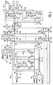
- FIG. 2 there is illustrated an embodiment of the invention using bipolar integrated circuit technology.
- a plurality of fuse links 14 are shown arranged in a two dimensional array of M+1 rows, numbered 0 to M, by N+1 columns, numbered 0 to N.
- links 14 are oriented vertically, having an upper terminal 14a and a lower terminal 14b.
- the array is arranged, for purposes of illustration, with rows oriented vertically and columns oriented horizontally.
- Each link 14 has an individual transistor switch 16 connected between the link's upper terminal 14a and a supply voltage source VCC, preferably equal to 5 volts.
- the base electrodes 16a of the transistor switches 16 connected to links 14 in each same row are connected to a row selection line 18 fed by a row decoder 20 for that row.
- Each row decoder 20 includes an AND gate 22 which is responsive to a group of parallel inputs 24, which are all digital ONE when the row number corresponding to the row is decoded and a further input signal VPROG at input 25 which is digital ONE to enable programming or verifying the states of the links 10. It should be appreciated that when all inputs to AND gate 22 of a row decoder are digital ONE, all transistor switches 16 controlled by that row decoder are in an ON state.
- each column decoder 28 includes a transistor switch 30 for producing a programming current I P through a selected link 14 to produce sufficient thermal energy in the link to cause it to become "open".
- Transistor 30 has its base electrode 30a connected to the output of an AND gate 31.
- each column decoder includes a switchable two level verification current source 32 including a first portion 34 for producing a relatively high level verification current I H , preferably 1ma, through the selected link and a second portion 36 for producing a relatively low level verification current I L , preferably 20 ⁇ a, through the selected link.
- the second portion in order to produce the low level verification current I L through the selected link, the second portion must actually sink a current equal to I L +I 1 , where I 1 is the current passing through a Schottky diode 66 coupling each column control line 26 to comparator circuitry which will be later discussed.
- Each column decoder 28 has a group of parallel inputs 38 which are all digital ONE in response to decoding of the column number corresponding to the column controlled by the column decoder, a PRO/VER input signal on input 40 which is near VCC (digital ONE) to enable programming and near ground (digital ZERO) to enable verification and the signal VPROG on input 42.
- the latter is near VCC (digital ONE) for programming and for verification.
- the inputs 38 feed an AND gate 44.
- a pulsatile signal VPROG on input 42 is coupled via a resistor 46 to a point 48 that is connected to the output of AND gate 44 so as to form a wired AND function.
- the PRO/VER input signal on input 40 and the output of AND gate 44 are inputs to AND gate 31 controlling transistor switch 30.
- the voltage at point 48 forms the supply voltage coupled via resistors 50, 52 to the collectors and bases of Schottky transistors 54, 56 and bases of Schottky transistors 58, 60, in the current source portions 34, 36, respectively.
- the emitters of the transistors 54, 56, 58, and 60 are all connected to PRO/VER input 40.
- Transistors 54, 58 and 56, 60 form input and output of current mirror pairs.
- the resistors 50, 52 and relative widths or number of parallel junctions of the current mirror pairs are chosen to achieve the current I H in transistor 58 and the current I L in transistor 60.
- the collector of output transistor 58 is connected to column control line 26 via the series combination of a Schottky diode 62 and two diodes formed by base to collector commoned transistors 64, while the collector of transistor 56 is directly connected to line 26.
- a link whose state is to be programmed or verified is selected by provision of its row and column locations to row and column decoders 20, 28 and the assertion of a VPROG pulse of digital ONE value.
- the transistor switches 16 of the selected row are turned on in response to row decoder 20 for that row and the transistor switch 30, for programming, or the two level current source 32, for verification, within the column decoder 28 for the selected column is turned on to sink current from its associated column conductor 26.
- Two level current source 32 is turned on for verification purposes during the duration of the VPROG pulse when the PRO/VER input is digital ZERO (near ground) while transistor switch 30 is turned on for programming purposes during the duration of the VPROG pulse when the PRO/VER input is digital ONE.
- the current produced through the selected link by two level current source 32 is dependent upon the link resistance.
- a link resistance greater than or equal to 75K ⁇ (1.5 volts/20 ⁇ a)
- only the lower current level I L will flow through the selected link, producing a link voltage across the selected link of greater than or equal to 1.5 volts.
- the voltage at the lower terminal 14b and conductor 26 will be 2.25 volts, which value is hereafter referred to as the lower reference voltage V 1 .
- the high current level I H of 1 ma will produce a link voltage of less than 1.5 volts. Consequently, the potential of terminal 14b will greater than 2.75 volts and transistor 58 will never be cut off.
- the voltage at lower terminal 14b will be 3.75 volts, the value thereof being referred to as the higher reference voltage V 2 .
- high level current source 34 will act to clamp the voltage of the lower terminal 14b to just below 2.75 volts.
- the various column control lines 26 are connected to the cathodes via Schottky diodes 66 whose anodes are connected to a common node 68.
- the effect of this interconnection is that the voltage at node 68 is due to the voltage at the lower terminal 14b of the selected link.
- a further Schottky diode whose anode is connected to node 68 forms a measurement voltage V MEAS at its cathode.
- the diode 66 associated with the selected column and the diode 68 are biased by current sources 72, 74 and 76 to have equal anode to cathode currents I 1 and consequently equal and opposite voltages. Therefore, measurement voltage V MEAS is equal to the voltage at the lower terminal 14b of the selected link.
- the current sources and differential comparators 78 and 80 are powered from a voltage source 83 which is active and equal to VCC only during a verification cycle.
- Voltage V MEAS is compared in differential comparator 78 with the lower reference voltage V 1 , which is formed by passing a current having the value I L through a resistance having the value R H which is connected to supply 83 via a Vbe junction. If V MEAS exceeds V 1 , which means the resistance of the link is less than R H , output 82 of comparator 78 will be high (digital ONE). Similarly, voltage V MEAS is compared in differential comparator 80 with the higher reference voltage V 2 . which is formed by passing a current having the value I H through a resistance having the value R L which is connected to supply 83 via a Vbe junction. If V MEAS exceeds V 2 which means the resistance of the link is less than R L , output 82 of comparator 78 will be high (digital ONE).
- Outputs 82 and 84 form the inputs of an AND gate 86 and of an Exclusive NOR gate 88.
- the output of gate 86 is digital ONE when both inputs are digital ONE, which corresponds to the resistance of the link being less than R L .
- the output of gate 88 is digital one when both inputs have the same digital value, which corresponds to the link resistance being greater than or equal to R H or less than R L . It should be appreciated that from these two digital outputs, it can be determined whether the state of the link is "validly open” (link resistance greater than or equal to R H ), “validly closed” (link resistance less than R L ), or “invalid” (link resistance greater than or equal to R L and less than R H ).
- FIG. 3 there is illustrated an embodiment of the invention using biCMOS integrated circuit technology.
- the same reference numerals are used for elements corresponding to the bipolar embodiment shown in Figure 1.
- the biCMOS embodiment differs from the bipolar embodiment in the design of the two level verification current source and in the voltage measuring section because the low level current I L and high level current I H are sequentially applied through the selected link under the control of a strobe signal and the result of comparison of the resultant two measurement values with the associated voltage reference values V 1 and V 2 are latched.
- low level current I L is produced through the selected link when the strobe signal is low (digital ZERO) while high level current I H is produced through the selected link when the strobe signal is high (digital ONE).
- the switchable two level verification current source 132 within each column decoder is formed by a pair of series connected FET's 202, 204.
- FET 202 has its gate electrode connected to output of AND gate 44 turning FET 202 on when the selected column is decoded by AND gate 44.
- the gate electrodes 204a of FET's 204 are connected together and are fed by line 216 output from column decoders controller 206.
- Controller 206 controls the current through a FET 218 to selectively add a high current I H to the low current I L +I 1 flowing in the drain to source path of FET 218.
- Line 216 connected to the commoned drain and gate of FET 216 has a voltage which causes FET 204 to have a drain to source current mirroring the current flowing in FET 218.
- Controller 206 is responsive to the output of an NOR gate 208 which receives a strobe signal on input 210 and the PRO/VER signal on input 212. It includes a voltage controlled current source 214 between voltage source 83 and line 216 producing I H , FET 218 between line 216 and ground, and current source 220 between source 83 and line 216 producing the low current I L +I 1 . Current due to I L +I 1 flows into the drain to source path of FET 218 whenever voltage source 83 is active, irrespective of the state of the strobe signal.
- the PRO/VER signal is digital ZERO during verification, as long as the strobe signal is digital ZERO, the output of NOR gate 208 will be digital ZERO.
- the current source 214 will be off and solely the current I L +I 1 will flow in the drain to source path of FET 218, and by current mirror action, also in the drain to source path of FET 204.
- a comparator 178 is provided which is identical to comparator 78 in Figure 2 except that a FET 222 is located for selectively activating comparator 178 when it is turned on.
- the gate electrode 222a of FET 222 is fed from the output of NOR gate 208, via an inverter 234, thereby turning FET 222 on when the output of NOR gate 208 is digital ZERO, which is when the strobe signal has not gone to digital ZERO.
- the output 82 of comparator 178 is applied via the series combination of an inverter 224 and gate element 226 to a latch 228 formed by cross coupled inverters 230, 232.
- comparator 180 is provided which is identical to comparator 80 in Figure 1 except that a FET 236a is located for selectively activating comparator 180 when it is turned on.
- the gate electrode 236a of FET 236 is fed directly from the output of NOR gate 208, thereby turning FET 236 on when the output of NOR gate 208 is digital ONE, which is when the strobe signal goes to digital ZERO.
- the output 84 of comparator 180 is applied via the series combination of an inverter 224 and gate element 240 to a latch 242 formed by cross coupled inverters 244, 246.
- Gate element 240 which is controlled opposite complementary inputs to gate element 226, is on when FET 236 is on.
- the output of latch 228 is digital ONE when the link resistance, as measured when the strobe is digital ONE, is less than the higher reference resistance value R H .
- the output of latch 242 is digital ONE when the link resistance, as measured when the strobe is digital ZERO, is less than the lower reference resistance value R L .
- verification circuitry being on-chip and physically merged with column decoder means.
- the verification circuitry or the switchable two-level current source may be part of off-chip test equipment.
- the invention then provides a method of verifying the status of an unprogrammed or programmed element whose basic step includes determining whether or not the value of the describing parameter lies in a forbidden range between two ranges of allowed parameter values.
Landscapes
- Tests Of Electronic Circuits (AREA)
- Logic Circuits (AREA)
- Design And Manufacture Of Integrated Circuits (AREA)
Claims (6)
- Elektronische Schaltung mit:einer Speicheranordnung aus programmierbaren Elementen, wobei jedes Element eine elektrische Eigenschaft aufweist, welche durch einen Parameter darstellbar ist und welche in Reaktion auf einen, auf das Element gerichteten Energieaufwand aus einem unprogrammierten Zustand heraus veränderbar ist, wobei der Parameter bei einem unprogrammierten Element einen, in einem ersten Wertebereich liegenden, ersten Wert und bei einem, mit Erfolg programmierten Element einen, in einem zweiten Wertebereich liegenden, zweiten Wert aufweist,
dadurch gekennzeichnet, dass die Schaltung aufweist:Prüfmittel, um ein ausgewähltes Element selektiv und reversibel in einen Prüfschaltkreis aufzunehmen und ein oder mehrere Signale zu liefern, welche darauf hinweisen, ob der Wert des Parameters des ausgewählten Elementes in einem unzulässigen Wertebereich des sich zwischen dem ersten und zweiten Bereich befindlichen Parameters liegt oder nicht. - Schaltung nach Anspruch 1, wobei die Prüfmittel eingesetzt werden, um ein bzw. mehrere Signale zu liefern, welche den, in einem bestimmten, ersten, zweiten oder unzulässigen Bereich liegenden Wert des Parameters des ausgewählten Elementes anzeigen.
- Schaltung nach Anspruch 1 oder 2, wobei der Parameter durch einen Widerstand dargestellt ist und die Prüfmittel aufweisen:eine Stromquelle, welche an das ausgewählte Element anschließbar ist und eingesetzt wird, um dem ausgewählten Element einen ersten bzw. zweiten Strom zur Erzeugung einer Spannung an dem ausgewählten Element zuzuführen, wobei der erste Strom wesentlich größer als der zweite Strom ist;an das ausgewählte Element gekoppelte Vergleichsmittel, um die Spannung mit der ersten und zweiten Referenzspannung, welche jeweils für den ersten und zweiten Bereich bezeichnend sind, zu vergleichen und für den Vergleich charakteristische Ausgangssignale des Komparators zu liefern;Logikgatemittel, um das Signal bzw. die mehreren Signale unter Zugrundelegung der Ausgangssignale des Komparators zu liefern.
- Schaltung nach Anspruch 3, wobei ein Verhältnis zwischen dem ersten und dem zweiten Strom in der Größenordnung von fünfzig liegt.
- Schaltung nach Anspruch 3 oder 4, wobei die Stromquelle eingesetzt wird, um den ersten Strom zu erzeugen, wenn das ausgewählte Element einen Widerstand aufweist, welcher kleiner als ein geringerer Referenzwert ist bzw. diesem entspricht, und um den zweiten Strom zu erzeugen, wenn das ausgewählte Element einen Widerstand aufweist, welcher größer als ein höherer Referenzwert ist bzw. diesem entspricht.
- Verfahren zum Prüfen eines Zustandes mehrerer programmierbarer Elemente in einer elektronischen Speicheranordnung, wobei jedes Element eine elektrische Eigenschaft aufweist, welche durch einen Parameter darstellbar ist und welche in Reaktion auf einen, auf das Element gerichteten Energieaufwand aus einem unprogrammierten Zustand heraus veränderbar ist, wobei der Parameter bei einem unprogrammierten Element einen, in einem ersten Wertebereich liegenden, ersten Wert und bei einem, mit Erfolg programmierten Element einen, in einem zweiten Wertebereich liegenden, zweiten Wert aufweist,
dadurch gekennzeichnet, dass der Prüfvorgang vorsieht:ein ausgewähltes Element in eine Prüfschaltung reversibel aufzunehmen;durch die Prüfschaltung ein oder mehrere Signale zu liefern, welche darauf hinweisen, ob der Wert des Parameters des ausgewählten Elementes in einem unzulässigen Wertebereich des sich zwischen dem ersten und zweiten Bereich befindlichen Parameters liegt oder nicht.
Applications Claiming Priority (3)
| Application Number | Priority Date | Filing Date | Title |
|---|---|---|---|
| US247934 | 1981-03-26 | ||
| US08/247,934 US5635854A (en) | 1994-05-24 | 1994-05-24 | Programmable logic integrated circuit including verify circuitry for classifying fuse link states as validly closed, validly open or invalid |
| PCT/IB1995/000339 WO1995032507A1 (en) | 1994-05-24 | 1995-05-09 | Programmable logic device with verify circuitry for classifying fuse link states as validly closed, validly open or invalid |
Publications (2)
| Publication Number | Publication Date |
|---|---|
| EP0711447A1 EP0711447A1 (de) | 1996-05-15 |
| EP0711447B1 true EP0711447B1 (de) | 2000-05-10 |
Family
ID=22936955
Family Applications (1)
| Application Number | Title | Priority Date | Filing Date |
|---|---|---|---|
| EP95915990A Expired - Lifetime EP0711447B1 (de) | 1994-05-24 | 1995-05-09 | Programmierbare logische vorrichtung mit einer prüfschaltung zum klassifizieren von schmelzverbindungszuständen als gültig geschlossen, gültig geöffnet oder ungültig |
Country Status (6)
| Country | Link |
|---|---|
| US (1) | US5635854A (de) |
| EP (1) | EP0711447B1 (de) |
| JP (1) | JP3662254B2 (de) |
| KR (1) | KR100395186B1 (de) |
| DE (1) | DE69516801T2 (de) |
| WO (1) | WO1995032507A1 (de) |
Families Citing this family (24)
| Publication number | Priority date | Publication date | Assignee | Title |
|---|---|---|---|---|
| US5694047A (en) * | 1995-08-09 | 1997-12-02 | Xilinx, Inc. | Method and system for measuring antifuse resistance |
| US5741720A (en) | 1995-10-04 | 1998-04-21 | Actel Corporation | Method of programming an improved metal-to-metal via-type antifuse |
| KR100236997B1 (ko) * | 1996-12-05 | 2000-01-15 | 정선종 | 오프셋 트리밍 장치 |
| US5859562A (en) * | 1996-12-24 | 1999-01-12 | Actel Corporation | Programming circuit for antifuses using bipolar and SCR devices |
| US6185705B1 (en) * | 1997-03-07 | 2001-02-06 | Micron Technology, Inc. | Method and apparatus for checking the resistance of programmable elements |
| US5952833A (en) | 1997-03-07 | 1999-09-14 | Micron Technology, Inc. | Programmable voltage divider and method for testing the impedance of a programmable element |
| KR100284904B1 (ko) * | 1998-05-29 | 2001-05-02 | 윤종용 | 불 휘발성 반도체 메모리 장치 및 그 장치의 무효 메모리 블록데이블 세팅 방법 |
| US6424161B2 (en) * | 1998-09-03 | 2002-07-23 | Micron Technology, Inc. | Apparatus and method for testing fuses |
| US6388305B1 (en) | 1999-12-17 | 2002-05-14 | International Business Machines Corporation | Electrically programmable antifuses and methods for forming the same |
| JP2002203901A (ja) * | 2000-12-27 | 2002-07-19 | Toshiba Microelectronics Corp | フューズ回路 |
| KR100761399B1 (ko) * | 2000-12-30 | 2007-09-27 | 주식회사 하이닉스반도체 | 리던던시 회로 |
| JP3932815B2 (ja) * | 2001-03-09 | 2007-06-20 | 株式会社デンソー | センサ回路網の異常検出方法 |
| US6541983B2 (en) * | 2001-05-10 | 2003-04-01 | Koninklijke Philips Electronics N.V. | Method for measuring fuse resistance in a fuse array |
| DE10162306A1 (de) * | 2001-12-19 | 2003-07-03 | Philips Intellectual Property | Verfahren und Anordnung zur Verifikation von NV-Fuses sowie ein entsprechendes Computerprogrammprodukt und ein entsprechendes computerlesbares Speichermedium |
| US6690193B1 (en) * | 2002-08-26 | 2004-02-10 | Analog Devices, Inc. | One-time end-user-programmable fuse array circuit and method |
| DE10319273B4 (de) * | 2003-04-29 | 2008-11-06 | Infineon Technologies Ag | Verfahren und Vorrichtung zum Bewerten und Nachprogrammieren von einmal programmierbaren Zellen |
| US20050254189A1 (en) * | 2004-05-07 | 2005-11-17 | Taiwan Semiconductor Manufacturing Co., Ltd. | ESD protection circuit with low parasitic capacitance |
| US7136322B2 (en) * | 2004-08-05 | 2006-11-14 | Analog Devices, Inc. | Programmable semi-fusible link read only memory and method of margin testing same |
| JP3923982B2 (ja) * | 2005-01-12 | 2007-06-06 | 株式会社東芝 | 半導体集積回路 |
| JP2006339290A (ja) * | 2005-05-31 | 2006-12-14 | Nec Electronics Corp | ヒューズ切断テスト回路及びヒューズ切断テスト方法並びに半導体回路 |
| US8072834B2 (en) | 2005-08-25 | 2011-12-06 | Cypress Semiconductor Corporation | Line driver circuit and method with standby mode of operation |
| TWI269306B (en) * | 2005-12-16 | 2006-12-21 | Fortune Semiconductor Corp | One-time programmable memory and its data recording method |
| US8223575B2 (en) * | 2007-03-08 | 2012-07-17 | Taiwan Semiconductor Manufacturing Co., Ltd. | Multi-level electrical fuse using one programming device |
| US7911820B2 (en) * | 2008-07-21 | 2011-03-22 | International Business Machines Corporation | Regulating electrical fuse programming current |
Family Cites Families (15)
| Publication number | Priority date | Publication date | Assignee | Title |
|---|---|---|---|---|
| JPS58164099A (ja) * | 1982-03-25 | 1983-09-28 | Toshiba Corp | 半導体メモリ− |
| JPS59175090A (ja) * | 1983-03-24 | 1984-10-03 | Toshiba Corp | 半導体記憶回路 |
| JPS60182219A (ja) * | 1984-02-29 | 1985-09-17 | Fujitsu Ltd | 半導体装置 |
| US4625162A (en) * | 1984-10-22 | 1986-11-25 | Monolithic Memories, Inc. | Fusible link short detector with array of reference fuses |
| US4814646A (en) * | 1985-03-22 | 1989-03-21 | Monolithic Memories, Inc. | Programmable logic array using emitter-coupled logic |
| US4698589A (en) * | 1986-03-21 | 1987-10-06 | Harris Corporation | Test circuitry for testing fuse link programmable memory devices |
| US4730273A (en) * | 1986-04-03 | 1988-03-08 | Motorola, Inc. | On-chip programmability verification circuit for programmable read only memory having lateral fuses |
| FR2660795B1 (fr) * | 1990-04-10 | 1994-01-07 | Sgs Thomson Microelectronics Sa | Circuit de detection de fusible. |
| US5140554A (en) * | 1990-08-30 | 1992-08-18 | Texas Instruments Incorporated | Integrated circuit fuse-link tester and test method |
| DE4041959A1 (de) * | 1990-12-24 | 1992-06-25 | Mikroelektronik Und Technologi | Schaltungsanordnung zur erkennung des programmierzustandes von durchbrennelementen |
| GB2253489B (en) * | 1991-03-06 | 1995-06-07 | Motorola Inc | Programmable read only memory |
| JP3379761B2 (ja) * | 1991-07-02 | 2003-02-24 | 株式会社日立製作所 | 不揮発性記憶装置 |
| US5293133A (en) * | 1992-08-27 | 1994-03-08 | Quicklogic Corporation | Method of determining an electrical characteristic of an antifuse and apparatus therefor |
| US5404049A (en) * | 1993-11-02 | 1995-04-04 | International Business Machines Corporation | Fuse blow circuit |
| US5453696A (en) * | 1994-02-01 | 1995-09-26 | Crosspoint Solutions, Inc. | Embedded fuse resistance measuring circuit |
-
1994
- 1994-05-24 US US08/247,934 patent/US5635854A/en not_active Expired - Lifetime
-
1995
- 1995-05-09 EP EP95915990A patent/EP0711447B1/de not_active Expired - Lifetime
- 1995-05-09 DE DE69516801T patent/DE69516801T2/de not_active Expired - Lifetime
- 1995-05-09 WO PCT/IB1995/000339 patent/WO1995032507A1/en not_active Ceased
- 1995-05-09 KR KR1019960700327A patent/KR100395186B1/ko not_active Expired - Fee Related
- 1995-05-09 JP JP53016595A patent/JP3662254B2/ja not_active Expired - Fee Related
Also Published As
| Publication number | Publication date |
|---|---|
| KR100395186B1 (ko) | 2003-11-28 |
| JPH09500971A (ja) | 1997-01-28 |
| JP3662254B2 (ja) | 2005-06-22 |
| DE69516801T2 (de) | 2000-11-30 |
| WO1995032507A1 (en) | 1995-11-30 |
| EP0711447A1 (de) | 1996-05-15 |
| DE69516801D1 (de) | 2000-06-15 |
| KR960704323A (ko) | 1996-08-31 |
| US5635854A (en) | 1997-06-03 |
Similar Documents
| Publication | Publication Date | Title |
|---|---|---|
| EP0711447B1 (de) | Programmierbare logische vorrichtung mit einer prüfschaltung zum klassifizieren von schmelzverbindungszuständen als gültig geschlossen, gültig geöffnet oder ungültig | |
| US4698589A (en) | Test circuitry for testing fuse link programmable memory devices | |
| US5412594A (en) | Fuse trimming in plastic package devices | |
| KR910003147B1 (ko) | 반도체집적회로와 그 시험방법 | |
| US4969124A (en) | Method for vertical fuse testing | |
| US6548884B2 (en) | Semiconductor device | |
| US7307911B1 (en) | Apparatus and method for improving sensing margin of electrically programmable fuses | |
| WO2006017416A2 (en) | Programmable semi-fusible link read only memory and method of margin testing same | |
| JPH0269684A (ja) | 集積回路の電源線試験方法 | |
| US7333383B2 (en) | Fuse resistance read-out circuit | |
| US5453696A (en) | Embedded fuse resistance measuring circuit | |
| EP0188013B1 (de) | Kurzschlussdetektor für durchbrennbare Schaltbrücken mit einer Anordnung von Referenzschaltbrücken | |
| US4707806A (en) | Semiconductor integrated circuit device having fuse-type information storing circuit | |
| US4806793A (en) | Signature circuit responsive to an input signal | |
| EP0173357B1 (de) | Binärschaltung mit wählbarer Ausgangspolarität | |
| US7453717B2 (en) | Three-state memory cell | |
| US4716547A (en) | Current switch for programming vertical fuses of a read only memory | |
| EP0011974A1 (de) | Mit Prüfmitteln ausgerüstete programmierbare Speichervorrichtung | |
| EP0911832B1 (de) | Speicherzelle mit programmierter Spielraumprüfung | |
| US4703455A (en) | Bipolar programmable memory and method | |
| JPS59919B2 (ja) | 半導体記憶装置 | |
| EP0228283A2 (de) | Halbleiterspeicher mit einer Prüfschaltung | |
| JP2002015594A (ja) | ヒューズブロー対応型の半導体集積回路 | |
| JPH0298893A (ja) | 半導体メモリ装置 | |
| JPH08274176A (ja) | 半導体装置 |
Legal Events
| Date | Code | Title | Description |
|---|---|---|---|
| PUAI | Public reference made under article 153(3) epc to a published international application that has entered the european phase |
Free format text: ORIGINAL CODE: 0009012 |
|
| AK | Designated contracting states |
Kind code of ref document: A1 Designated state(s): DE FR GB NL |
|
| 17P | Request for examination filed |
Effective date: 19960530 |
|
| RAP3 | Party data changed (applicant data changed or rights of an application transferred) |
Owner name: KONINKLIJKE PHILIPS ELECTRONICS N.V. |
|
| GRAG | Despatch of communication of intention to grant |
Free format text: ORIGINAL CODE: EPIDOS AGRA |
|
| 17Q | First examination report despatched |
Effective date: 19990809 |
|
| GRAG | Despatch of communication of intention to grant |
Free format text: ORIGINAL CODE: EPIDOS AGRA |
|
| GRAH | Despatch of communication of intention to grant a patent |
Free format text: ORIGINAL CODE: EPIDOS IGRA |
|
| GRAH | Despatch of communication of intention to grant a patent |
Free format text: ORIGINAL CODE: EPIDOS IGRA |
|
| GRAA | (expected) grant |
Free format text: ORIGINAL CODE: 0009210 |
|
| AK | Designated contracting states |
Kind code of ref document: B1 Designated state(s): DE FR GB NL |
|
| PG25 | Lapsed in a contracting state [announced via postgrant information from national office to epo] |
Ref country code: NL Free format text: LAPSE BECAUSE OF FAILURE TO SUBMIT A TRANSLATION OF THE DESCRIPTION OR TO PAY THE FEE WITHIN THE PRESCRIBED TIME-LIMIT Effective date: 20000510 |
|
| REF | Corresponds to: |
Ref document number: 69516801 Country of ref document: DE Date of ref document: 20000615 |
|
| ET | Fr: translation filed | ||
| NLV1 | Nl: lapsed or annulled due to failure to fulfill the requirements of art. 29p and 29m of the patents act | ||
| PLBE | No opposition filed within time limit |
Free format text: ORIGINAL CODE: 0009261 |
|
| STAA | Information on the status of an ep patent application or granted ep patent |
Free format text: STATUS: NO OPPOSITION FILED WITHIN TIME LIMIT |
|
| 26N | No opposition filed | ||
| REG | Reference to a national code |
Ref country code: GB Ref legal event code: IF02 |
|
| REG | Reference to a national code |
Ref country code: FR Ref legal event code: D6 |
|
| REG | Reference to a national code |
Ref country code: GB Ref legal event code: 746 Effective date: 20021107 |
|
| REG | Reference to a national code |
Ref country code: GB Ref legal event code: 732E |
|
| REG | Reference to a national code |
Ref country code: FR Ref legal event code: TP |
|
| REG | Reference to a national code |
Ref country code: FR Ref legal event code: ST Effective date: 20090119 |
|
| PG25 | Lapsed in a contracting state [announced via postgrant information from national office to epo] |
Ref country code: FR Free format text: LAPSE BECAUSE OF NON-PAYMENT OF DUE FEES Effective date: 20080602 |
|
| REG | Reference to a national code |
Ref country code: FR Ref legal event code: D3 |
|
| PGFP | Annual fee paid to national office [announced via postgrant information from national office to epo] |
Ref country code: DE Payment date: 20100512 Year of fee payment: 16 |
|
| PGFP | Annual fee paid to national office [announced via postgrant information from national office to epo] |
Ref country code: FR Payment date: 20110621 Year of fee payment: 17 |
|
| PGFP | Annual fee paid to national office [announced via postgrant information from national office to epo] |
Ref country code: GB Payment date: 20110503 Year of fee payment: 17 |
|
| GBPC | Gb: european patent ceased through non-payment of renewal fee |
Effective date: 20120509 |
|
| REG | Reference to a national code |
Ref country code: FR Ref legal event code: ST Effective date: 20130131 |
|
| REG | Reference to a national code |
Ref country code: DE Ref legal event code: R119 Ref document number: 69516801 Country of ref document: DE Effective date: 20121201 |
|
| PG25 | Lapsed in a contracting state [announced via postgrant information from national office to epo] |
Ref country code: GB Free format text: LAPSE BECAUSE OF NON-PAYMENT OF DUE FEES Effective date: 20120509 Ref country code: FR Free format text: LAPSE BECAUSE OF NON-PAYMENT OF DUE FEES Effective date: 20120531 |
|
| PG25 | Lapsed in a contracting state [announced via postgrant information from national office to epo] |
Ref country code: DE Free format text: LAPSE BECAUSE OF NON-PAYMENT OF DUE FEES Effective date: 20121201 |