EP0706147B1 - Digitaliseur avec réduction de bruit - Google Patents
Digitaliseur avec réduction de bruit Download PDFInfo
- Publication number
- EP0706147B1 EP0706147B1 EP95306976A EP95306976A EP0706147B1 EP 0706147 B1 EP0706147 B1 EP 0706147B1 EP 95306976 A EP95306976 A EP 95306976A EP 95306976 A EP95306976 A EP 95306976A EP 0706147 B1 EP0706147 B1 EP 0706147B1
- Authority
- EP
- European Patent Office
- Prior art keywords
- grid
- shield
- signal
- noise
- coupling
- Prior art date
- Legal status (The legal status is an assumption and is not a legal conclusion. Google has not performed a legal analysis and makes no representation as to the accuracy of the status listed.)
- Expired - Lifetime
Links
Images

Classifications
-
- G—PHYSICS
- G06—COMPUTING; CALCULATING OR COUNTING
- G06F—ELECTRIC DIGITAL DATA PROCESSING
- G06F3/00—Input arrangements for transferring data to be processed into a form capable of being handled by the computer; Output arrangements for transferring data from processing unit to output unit, e.g. interface arrangements
- G06F3/01—Input arrangements or combined input and output arrangements for interaction between user and computer
- G06F3/03—Arrangements for converting the position or the displacement of a member into a coded form
- G06F3/041—Digitisers, e.g. for touch screens or touch pads, characterised by the transducing means
- G06F3/0416—Control or interface arrangements specially adapted for digitisers
- G06F3/0418—Control or interface arrangements specially adapted for digitisers for error correction or compensation, e.g. based on parallax, calibration or alignment
- G06F3/04182—Filtering of noise external to the device and not generated by digitiser components
-
- G—PHYSICS
- G06—COMPUTING; CALCULATING OR COUNTING
- G06F—ELECTRIC DIGITAL DATA PROCESSING
- G06F3/00—Input arrangements for transferring data to be processed into a form capable of being handled by the computer; Output arrangements for transferring data from processing unit to output unit, e.g. interface arrangements
- G06F3/01—Input arrangements or combined input and output arrangements for interaction between user and computer
- G06F3/03—Arrangements for converting the position or the displacement of a member into a coded form
-
- G—PHYSICS
- G06—COMPUTING; CALCULATING OR COUNTING
- G06F—ELECTRIC DIGITAL DATA PROCESSING
- G06F2203/00—Indexing scheme relating to G06F3/00 - G06F3/048
- G06F2203/041—Indexing scheme relating to G06F3/041 - G06F3/045
- G06F2203/04107—Shielding in digitiser, i.e. guard or shielding arrangements, mostly for capacitive touchscreens, e.g. driven shields, driven grounds
-
- G—PHYSICS
- G06—COMPUTING; CALCULATING OR COUNTING
- G06F—ELECTRIC DIGITAL DATA PROCESSING
- G06F3/00—Input arrangements for transferring data to be processed into a form capable of being handled by the computer; Output arrangements for transferring data from processing unit to output unit, e.g. interface arrangements
- G06F3/01—Input arrangements or combined input and output arrangements for interaction between user and computer
- G06F3/03—Arrangements for converting the position or the displacement of a member into a coded form
- G06F3/041—Digitisers, e.g. for touch screens or touch pads, characterised by the transducing means
- G06F3/044—Digitisers, e.g. for touch screens or touch pads, characterised by the transducing means by capacitive means
Definitions
- the present invention relates to digitizer apparatus and in particular to digitizer apparatus with noise reduction means.
- Digitizing tablet sensor circuits can be adversely affected by ambient electrical and electrostatic noise from light sources, display monitors, and nearby electrically operated devices. Severe interference can be caused by image generators such as television screens or computer monitor screens when a digitizing grid is placed over the screen for digitizing a generated image.
- prior art systems insert a conductive shield between possible noise sources and the sensors.
- the shield is grounded to conduct electrical noise away.
- Several examples of the prior art illustrate this approach to eradicating unwanted noise and electrostatic interference.
- U.S. Patent 4,644,102 shows the use of an electrostatic shield using grounded copper strips and a grounded copper plate.
- the grounded copper strips prevent the effects of reversed fields that occur when using a conventional grounded plate. Noise is eliminated or at least reduced by the use of a demodulator coupled to a matched filter instead of a conventional low-pass filter which was considered to have too slow a recovery time.
- U.S. Patent 4,636,582 teaches the use of a conductive shield layer coupled to ground to prevent electrostatic interference with handwritten information detected by a pair of conductive layers activated by a writing stylus. Electrostatic noise from the hand of a user or nearby electrical devices interferes with the decoding of signals representing entered information.
- the shield is intended to ground at least some of the electrical noise.
- U.S. Patent 4,497,977 shows the use of an electrostatic shield layer coupled to ground to prevent noise from the hand of a user from causing interference with electrical signals representing information entered via a handheld stylus.
- U.S. Patent 3,974,332 describes a system for entering information using a conductive pen capacitively coupled to a tablet for selecting segments on the tablet.
- the segments are insulated from one another by an electrically conductive grounded shield layer with apertures for the segments.
- the shield prevents capacitive coupling to segments adjacent to a selected segment, i.e., prevents or at least reduces crosstalk between segments.
- U.S. Patent 3,732,369 shows a digitizing tablet having x- and y-coordinate wires that are capacitively coupled to a stylus for supplying signals indicative of the x,y position of the stylus.
- a conductive ground plane, insulated from the lower wires, is provided.
- U.S. Patent 4,956,526 describes the use of a shielding plate placed at a distance from a sensor plate to provide a maximum output voltage signal.
- U.S. Patent 4,853,497 teaches the use of pan-shaped nonferrous shield that extends over and close to the sides of a rectangular grid of wires in an electromagnetic digitizer to eliminate edge effects.
- U.S. Patent 5,124,509 describes a digitizing device having a conductive plate in an inductively coupled system.
- the purpose of the plate is not to eliminate or to reduce interference noise. It operates to detect a submultiple of the stylus' oscillator frequency, the latter being used to induce a voltage signal in the associated grid lines.
- the submultiple frequency is capacitively coupled from the stylus to the user's hand or body.
- the plate picks up the submultiple frequency and couples it through a phase-locked loop to operate an analog switch.
- the conductivity of the plate is purposely made low. Also shown is a prior art standard grounded electrostatic shield.
- U.S. Patent 5,218,173 relates to materials used in shields for electromagnetic digitizers such as used in notebook computers.
- the shield plate protects the circuitry from local interference and magnetic fields such as those created by power transformers and the like.
- US patent 4859814 discloses a digitizer apparatus in which noise emitted by image source means (CRT) is reduced by a differential noise reduction technique which consists in differentially amplifying a sensing signal from a conductive wire of a grid and a noise signal from a noise reference conductor.
- the noise reference conductor can be another conductive wire of the grid or another "noise antenna".
- the noise antenna could also have a function of shielding of the grid from noise emitted by the CRT.
- the present invention seeks to provide for digitizer apparatus having advantages over known digitizer apparatus.
- digitizer apparatus according to claim 1.
- a noise shield in a digitizing tablet can be coupled to ground through a circuit that produces electrical signals proportional to interfering noise and applies the extracted signals to the desired output signal so as to cancel the noise from such output signal.
- the shield can be grounded at one point and a noise signal taken from a point on an ungrounded edge of the shield.
- a conductive shield between an image source and a digitizing grid so that the electrostatic noise impressed on the digitizing grid is a duplicate of or is congruent with that which is impressed on the shield (except for possible differences in amplitude).
- the shield can be coupled to ground through an impedance to develop a voltage proportional to the noise potential.
- the voltage so developed across the impedance is applied to a differential amplifier as is the signal from the digitizing grid so as to supply an output signal proportional to the digitizing grid signal with the noise signal component cancelled.
- the invention is advantageous in supplying a noise cancellation signal. Also, the invention can improve the performance of electrostatic shielding by cancelling noise from the output signal.
- the shield can also be grounded on one or more sides leaving at least one side or edge ungrounded. A voltage potential can be tapped from the ungrounded side to supply the noise-proportional signal to the differential amplifier.
- the noise signal can be conducted to the cancelling circuit via a matching or phase shift network, which may be made adjustable for improving noise cancellation since at least part of the electrical noise may be capacitively coupled to the shield causing a phase shift between the signals on the grid and noise shield.
- a matching or phase shift network which may be made adjustable for improving noise cancellation since at least part of the electrical noise may be capacitively coupled to the shield causing a phase shift between the signals on the grid and noise shield.
- reference to supplying signals from a digitizing grid should be understood to include the case where the signal is taken from the grid per se (U.S. Patents 4,644,102 and 5,124,509) or from a stylus inductively, capacitively, or otherwise coupled to the grid (U.S. Patent 3,732,369).
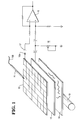
- FIG. 1 Principal elements of one embodiment of the present invention, and their interconnection, are illustrated in FIG. 1.
- a digitizing grid 10 is coupled, via connectors 15a and 17, to an amplifier 16 which includes suitable input and feedback resistors in a manner well known in the art.
- a transparent conductive shield 12 is interposed between the digitizing grid 10 and an image plane 14.
- the image plane 14 and a light source 19 can be any type of image source or image generator, e.g., a television screen or a computer monitor screen. It is well known that such image generators produce substantial amounts of electrical noise interference which prior art grounded plates cannot shield.
- the shield 12 and the digitizing grid 10 are spaced so that electrostatic noise passing through the shield 12 to the digitizing grid 10 will be substantially congruent or similar to the noise intercepted by the shield 10.
- the distance of the spacing between the shield 12 and the digitizing grid 10 is limited by two principal factors. If the spacing is too small, the shield 12 and the digitizing grid 10 form a capacitor which becomes more effective in passing noise signals the closer they are together. If the spacing is too large, a depth field is created and the resulting parallax distortion will cause misplacement of the pen or probe 11 with respect to the image points being digitized. The spacing appears to be optimal between one and two millimetres.
- the shield 12 may even be implemented as a coating on the face of the display 14, e.g., a cathode ray tube face.
- the shield 12 may be fabricated from an indium-tin-oxide (ITO) material, such as is used commercially in the manufacture of liquid crystal displays, because of its transparency and electrical characteristics.
- ITO indium-tin-oxide
- the shield 12 is coupled to a phase shift network 18 which may be constructed to allow the phase and amplitude of the noise signal from the shield 12 to be adjusted over a desired range.
- the phase-adjusted signal from the network 18 is coupled to another input of the amplifier 16 through suitable resistors.
- the signals are coupled to the amplifier 16 so that a signal corresponding the noise signal from the shield 12 is cancelled from the signal from the digitizing grid 10 which includes both noise and information components.
- electrostatic and other electrical noise that are included in the signal from the digitizing grid 10, due principally to the image generator 14, will be similar or congruent to that from the shield 12.
- the noise signals from the image generator 14 are somewhat attenuated by passing through the shield 12 but because the shield 12 is not ideal, e.g. having a poor ground impedance, some noise signals will be passed and picked up on the digitizing grid 10.
- the amplitude of the noise signal taken from the shield 12 will normally be larger than the amplitude of the corresponding signal on the digitizing grid 10. Differences in the amplitudes of the noise signals taken from the shield 12 and the digitizing grid 10 can be compensated for by amplifying either signal or by adjusting the values of the resistors in the amplifier networks.
- FIGS. 2 and 3 Other useful means for coupling the noise from the shield 10 to the amplifier 16 to cancel the noise in the signal from the digitizing grid 10 are shown in FIGS. 2 and 3.
- the capacitors 21 and 23 represent the equivalent capacitances coupling noise to the shield 12 and to the digitizing grid 10 respectively.
- the equivalent resistance of the shield is represented by the resistor 25 which is coupled to ground through an inductor 27. Therefore, current created by the noise on the shield 12 passes through the inductor 27.
- the current through the inductor 27 induces a voltage in a proximate inductor 29 which is coupled to the amplifier 16 through a phase adjusting circuit comprising a capacitor 18a and a resistor 18b.
- the signal has the same noise coupled thereto by the equivalent capacitance 23 so that the input signal to the inverting input terminal of the amplifier 16 includes the noise.
- the output signal from the amplifier 16 does not include the noise since it is removed from the signal by coupling it to the non-inverting input terminal of the amplifier 16.
- the polarities of the input terminals can be of course reversed.
- the noise can be subtracted from the signal by reversing the polarity of the inductance 29 and coupling the signal from the phase adjustment circuit resistively to the inverting input terminal and coupling the non-inverting input terminal to ground.
- FIG. 3 Another coupling circuit is illustrated in FIG. 3.
- the equivalent capacitors 21 and 23 and the equivalent resistance 25 of the shield 12 are the same as described in connection with the circuit of FIG. 2.
- the electric current from the shield 12, i.e., from the resistor 25, is coupled via a capacitor 31 and a resistor 33 (which can be adjustable as shown) to ground.
- the voltage developed across the resistor 33 is coupled to the non-inverting input terminal of the amplifier 16 via a phase adjusting circuit comprising the capacitor 18a and the resistor 18b, as previously described in connection with the circuit of FIG. 2.
- Coupling the shield to ground through impedances can create unwanted signals in addition to the noise because the shield 12 is quasi-floating.
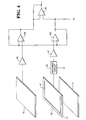
- the shield 12 can be grounded on three sides, as shown in FIG. 4, by a ground conductor 41 on the shield.
- the noise potential can then be taken from a tap point on the ungrounded side of the shield 10 and coupled to a noise amplifier 47 via a matching circuit 43.
- the matching circuit 43 can include a phase adjustment circuit as previously described.
- the noise amplifier 47 and a signal amplifier 45 can be provided as inverting operational amplifiers with suitable input and feedback resistors (not shown) or as unity gain amplifiers by coupling the output terminal to the inverting input terminal and coupling the input signal to the non-inverting input terminal.
- the latter arrangement provides an extremely high input impedance to the input noise and signal sources which helps to reduce signal distortion.
- the output signals from the signal amplifier 45 and from the noise amplifier 47 are coupled to amplifiers 401 and 403 coupled as a common mode rejection differential amplifier.
- the output signals from the amplifiers 401 and 403 are coupled to the output amplifier 16.
- This arrangement not only supplies a high input impedance for the signals but also rejects common mode noise to prevent distortion of the signals.
Claims (8)
- Appareil numériseur pour utiliser avec un stylet (11) et ayant une tablette graphique et une source d'images (13) pour fournir une image à afficher au moyen de ladite tablette, ladite tablette ayant une grille (10) pour fournir un signal en fonction de la position du stylet (11) par rapport à ladite tablette, et dans lequel ledit appareil a également un amplificateur différentiel (16) ayant une première et une seconde entrées, ledit signal fourni par ladite grille (10) étant ainsi délivré vers la première entrée, ledit appareil étant caractérisé par des moyens de blindage (12) pour blinder ladite grille (10) contre le bruit émis par ladite source d'images (13), pour fournir un signal dérivé à partir du bruit produit par ladite source d'images (14) à ladite seconde entrée dudit amplificateur différentiel.
- Appareil selon la Revendication 1, dans lequel ledit stylet (11) est agencé pour produire un signal représentatif d'une position du stylet (11) sur ladite tablette, ladite source d'images est agencée pour produire une image à numériser, ledit amplificateur différentiel (16) est agencé pour fournir un signal de sortie proportionnel à la différence entre les valeurs de signaux sur lesdites première et seconde entrées, ladite grille (10) est agencée pour détecter le signal émis par ledit stylet (11), lesdits moyens de blindage (12) englobent des moyens de blindage conducteur placés entre ladite source d'images (14) et ladite grille (10) et dans lequel un moyen de couplage (18) est prévu pour coupler un signal fourni par lesdits moyens de blindage (12) à ladite seconde entrée dudit amplificateur différentiel (16).
- Appareil selon la Revendication 2, dans lequel ledit moyen de couplage (18) englobe un moyen d'ajustement de phase.
- Appareil selon la Revendication 1, dans lequel ladite source d'images (14) est agencée pour produire une image à numériser, ladite grille (10) est agencée pour fournir un signal de sortie qui indique la position dudit stylet (11) sur la surface de ladite grille (16), ladite grille (10) étant positionnée au-dessus de ladite source d'images (14), lesdits moyens de blindage (12) englobant des moyens de blindage conducteur placés entre ladite grille (10) et ladite source d'images de façon telle que tout potentiel à bruit électrostatique exercé sur ladite grille à partir de ladite source d'images traverse lesdits moyens de blindage conducteur (12) et sert à fournir un signal proportionnel au potentiel à bruit électrostatique, ledit amplificateur différentiel (16) étant agencé pour fournir des signaux proportionnels à une différence entre les signaux d'entrée couplés auxdites première et seconde entrées de celui-ci, et englobant des moyens (41) de mise à la masse d'un bord des moyens de blindage conducteur (12), un premier moyen de couplage (43) pour coupler un bord non mis à la masse desdits moyens de blindage conducteur (12) à ladite seconde entrée dudit amplificateur différentiel (16) et un second moyen de couplage (45) pour coupler des signaux provenant de ladite grille (10) à ladite première entrée dudit amplificateur différentiel (16).
- Appareil selon la Revendication 1, 2, 3 ou 4, dans lequel lesdits moyens de blindage (12) sont transparents.
- Appareil selon la Revendication 4, dans lequel les bords 0 à n-1 desdits moyens de blindage conducteur (12) sont mis à la masse, n étant le nombre de bords sur lesdits moyens de blindage conducteur (12).
- Appareil selon la Revendication 4, dans lequel lesdits premier et second moyens de couplage englobent chacun un amplificateur d'isolement (45, 47).
- Appareil selon la Revendication 7, dans lequel ledit amplificateur différentiel (16) englobe un étage de réjection en mode commun (401, 403).
Applications Claiming Priority (2)
| Application Number | Priority Date | Filing Date | Title |
|---|---|---|---|
| US317952 | 1994-10-04 | ||
| US08/317,952 US5574262A (en) | 1994-10-04 | 1994-10-04 | Noise cancellation for non-ideal electrostatic shielding |
Publications (3)
| Publication Number | Publication Date |
|---|---|
| EP0706147A2 EP0706147A2 (fr) | 1996-04-10 |
| EP0706147A3 EP0706147A3 (fr) | 1996-05-01 |
| EP0706147B1 true EP0706147B1 (fr) | 2000-01-12 |
Family
ID=23235973
Family Applications (1)
| Application Number | Title | Priority Date | Filing Date |
|---|---|---|---|
| EP95306976A Expired - Lifetime EP0706147B1 (fr) | 1994-10-04 | 1995-10-02 | Digitaliseur avec réduction de bruit |
Country Status (5)
| Country | Link |
|---|---|
| US (1) | US5574262A (fr) |
| EP (1) | EP0706147B1 (fr) |
| JP (1) | JP3007560B2 (fr) |
| KR (1) | KR100399563B1 (fr) |
| DE (1) | DE69514471T2 (fr) |
Cited By (1)
| Publication number | Priority date | Publication date | Assignee | Title |
|---|---|---|---|---|
| US8614690B2 (en) | 2008-09-26 | 2013-12-24 | Apple Inc. | Touch sensor panel using dummy ground conductors |
Families Citing this family (40)
| Publication number | Priority date | Publication date | Assignee | Title |
|---|---|---|---|---|
| JP3188367B2 (ja) * | 1994-12-26 | 2001-07-16 | シャープ株式会社 | 座標検出装置 |
| KR100190160B1 (ko) * | 1995-10-27 | 1999-06-01 | 윤종용 | 디스플레이 기기의 전계 차폐 회로 |
| US5859392A (en) * | 1996-02-09 | 1999-01-12 | Lsi Logic Corporation | Method and apparatus for reducing noise in an electrostatic digitizing tablet |
| US5990865A (en) * | 1997-01-06 | 1999-11-23 | Gard; Matthew Davis | Computer interface device |
| US6081259A (en) * | 1997-11-25 | 2000-06-27 | Lsi Logic Corporation | Method and apparatus for reducing noise in an electrostatic digitizer |
| US7663607B2 (en) | 2004-05-06 | 2010-02-16 | Apple Inc. | Multipoint touchscreen |
| KR100272169B1 (ko) * | 1998-08-14 | 2000-11-15 | 윤종용 | 센서 패널의 위치 좌표 신호 검출회로 |
| JP2000181612A (ja) * | 1998-12-16 | 2000-06-30 | Fujitsu Takamisawa Component Ltd | 座標入力装置 |
| GB2373581B (en) * | 2001-03-20 | 2004-11-10 | Eturbotouch Technology Inc | Touch screen capable of isolating noise signals |
| US20030010544A1 (en) * | 2001-07-10 | 2003-01-16 | Ching-Chuan Chao | Low EMI digitizer tablet |
| KR100469355B1 (ko) * | 2002-11-14 | 2005-02-02 | 엘지.필립스 엘시디 주식회사 | 표시장치용 터치 패널 |
| US7678346B2 (en) | 2003-01-30 | 2010-03-16 | Gm Global Technology Operations, Inc. | Dual function CO clean-up/sorber unit |
| JP2007525761A (ja) | 2004-02-27 | 2007-09-06 | エヌ−トリグ リミテッド | デジタイザシステムにおけるノイズ低減 |
| JP4533259B2 (ja) * | 2005-06-29 | 2010-09-01 | アルプス電気株式会社 | 入力装置 |
| WO2007146785A2 (fr) | 2006-06-09 | 2007-12-21 | Apple Inc. | Affichage à cristaux liquides à écran tactile |
| US7920129B2 (en) | 2007-01-03 | 2011-04-05 | Apple Inc. | Double-sided touch-sensitive panel with shield and drive combined layer |
| US9710095B2 (en) * | 2007-01-05 | 2017-07-18 | Apple Inc. | Touch screen stack-ups |
| JP5051690B2 (ja) | 2007-01-30 | 2012-10-17 | 株式会社ジャパンディスプレイウェスト | 入力機能付表示装置 |
| US20080238881A1 (en) * | 2007-03-27 | 2008-10-02 | N-Trig Ltd. | Shield for a digitizer sensor |
| KR101587897B1 (ko) * | 2007-05-07 | 2016-01-25 | 삼성디스플레이 주식회사 | 터치 패널 일체형 액정 표시 장치 및 그 구동 방법 |
| US8174508B2 (en) * | 2007-11-19 | 2012-05-08 | Microsoft Corporation | Pointing and data entry input device |
| KR101237640B1 (ko) * | 2008-01-29 | 2013-02-27 | (주)멜파스 | 기생 캐패시턴스 방지 구조를 구비한 터치스크린 장치 |
| JP5264249B2 (ja) * | 2008-03-31 | 2013-08-14 | 三菱自動車工業株式会社 | 静電容量式タッチセンサー装置 |
| US9927924B2 (en) | 2008-09-26 | 2018-03-27 | Apple Inc. | Differential sensing for a touch panel |
| KR101657215B1 (ko) * | 2009-09-08 | 2016-09-19 | 삼성디스플레이 주식회사 | 터치 패널 장치를 포함하는 표시 장치 및 커플링 노이즈 제거 방법 |
| US9164620B2 (en) | 2010-06-07 | 2015-10-20 | Apple Inc. | Touch sensing error compensation |
| US8804056B2 (en) | 2010-12-22 | 2014-08-12 | Apple Inc. | Integrated touch screens |
| KR20130005660A (ko) * | 2011-07-07 | 2013-01-16 | 삼성전자주식회사 | 터치스크린패널 액정디스플레이장치 |
| US9259904B2 (en) | 2011-10-20 | 2016-02-16 | Apple Inc. | Opaque thin film passivation |
| FR2988553B1 (fr) * | 2012-03-23 | 2015-03-27 | Fogale Nanotech | Dispositif de detection capacitive integrant une piste metallique sur une garde transparente. |
| US10095361B2 (en) | 2015-03-18 | 2018-10-09 | Microsoft Technology Licensing, Llc | Stylus detection with capacitive based digitizer sensor |
| US9671913B2 (en) | 2015-05-11 | 2017-06-06 | Microsoft Technology Licensing, Llc | Capacitive display device |
| US10296146B2 (en) | 2015-12-22 | 2019-05-21 | Microsoft Technology Licensing, Llc | System and method for detecting grip of a touch enabled device |
| US10423268B2 (en) | 2015-12-22 | 2019-09-24 | Microsoft Technology Licensing, Llc | System and method for detecting grounding state of a touch enabled computing device |
| US9823774B2 (en) | 2016-02-23 | 2017-11-21 | Microsoft Technology Licensing, Llc | Noise reduction in a digitizer system |
| WO2018057969A1 (fr) | 2016-09-23 | 2018-03-29 | Apple Inc. | Panneau de capteur tactile à blindage supérieur et/ou inférieur |
| US10372282B2 (en) | 2016-12-01 | 2019-08-06 | Apple Inc. | Capacitive coupling reduction in touch sensor panels |
| US10678348B2 (en) | 2018-03-12 | 2020-06-09 | Microsoft Technology Licensing, Llc | Touch detection on an ungrounded pen enabled device |
| US10616349B2 (en) | 2018-05-01 | 2020-04-07 | Microsoft Technology Licensing, Llc | Hybrid sensor centric recommendation engine |
| US11789561B2 (en) | 2021-09-24 | 2023-10-17 | Apple Inc. | Architecture for differential drive and sense touch technology |
Family Cites Families (25)
| Publication number | Priority date | Publication date | Assignee | Title |
|---|---|---|---|---|
| US3732369A (en) * | 1971-04-05 | 1973-05-08 | Welland Investment Trust | Coordinate digitizer system |
| DE2508154C3 (de) * | 1974-12-03 | 1978-06-15 | Pentel K.K., Tokio | Eingabeplatte |
| US4185165A (en) * | 1978-07-03 | 1980-01-22 | Talos Systems, Inc. | Low noise system and method for sequentially sensing induced signals in digitizer grid conductors |
| US4456787A (en) * | 1982-07-06 | 1984-06-26 | Scriptel Corporation | Electrographic system and method |
| US4497977A (en) * | 1983-03-03 | 1985-02-05 | Kabushiki Kaisha Daini Seikosha | Automatic coordinate determining device having electrostatic shielding |
| US4636582A (en) * | 1983-08-31 | 1987-01-13 | Toppan Moore Co., Ltd. | Signal input sheet having a conductive shield layer |
| US4631355A (en) * | 1984-12-18 | 1986-12-23 | At&T Bell Laboratories | Telautograph system |
| US4644102A (en) * | 1985-03-29 | 1987-02-17 | Pencept, Inc. | Digitizing tablet system |
| US4736073A (en) * | 1986-02-10 | 1988-04-05 | Sanders Associates, Inc. | Noise-canceling system for a digitizing tablet |
| FR2608753B1 (fr) * | 1986-12-18 | 1991-06-07 | Centre Nat Rech Scient | Dispositif de localisation bidimensionnelle d'evenements generateurs de courant sur une surface resistive |
| US4853497A (en) * | 1988-06-20 | 1989-08-01 | Calcomp Inc. | Shielding techique for digitizers |
| US4859814A (en) * | 1988-08-29 | 1989-08-22 | Kurta Corporation | Noise cancellation in digitizing system and method |
| JPH02178822A (ja) * | 1988-12-29 | 1990-07-11 | Toppan Moore Co Ltd | 信号入力シート |
| US4956526A (en) * | 1989-07-18 | 1990-09-11 | Kabushikikaisha Wacom | Digitizer having flat tablet with magnetic shield plate |
| JPH0383120A (ja) * | 1989-08-28 | 1991-04-09 | Mitsubishi Electric Corp | 座標入力機能付表示装置 |
| US5008497A (en) * | 1990-03-22 | 1991-04-16 | Asher David J | Touch controller |
| US5083118A (en) * | 1990-04-16 | 1992-01-21 | Pentel Kabushiki Kaisha | Transparent coordinate input apparatus for electrostatic capacity coupling system |
| JPH0458316A (ja) * | 1990-06-28 | 1992-02-25 | Toshiba Corp | 情報処理装置 |
| US5124509A (en) * | 1991-01-15 | 1992-06-23 | Calcomp, Inc. | Digitizer with capacitive and inductive coupling |
| US5136125A (en) * | 1991-05-06 | 1992-08-04 | International Business Machines Corporation | Sensor grid for an electromagnetic digitizer tablet |
| US5218174A (en) * | 1991-10-01 | 1993-06-08 | Kurta Corporation | Low power cordless magnetic field digitizer with differential grid sensing and synchronous position demodulation |
| US5218173A (en) * | 1991-10-17 | 1993-06-08 | Ibm Corporation | Shielding materials for electromagnetic digitizers |
| JP2988779B2 (ja) * | 1992-05-20 | 1999-12-13 | シャープ株式会社 | 表示機能付きタブレット装置 |
| EP0589498A1 (fr) * | 1992-08-12 | 1994-03-30 | Koninklijke Philips Electronics N.V. | Circuit électronique rendu insensible aux parasites électromagnétiques d'un afficheur |
| JP3003895B2 (ja) * | 1992-09-09 | 2000-01-31 | 川崎重工業株式会社 | レーザ加工装置 |
-
1994
- 1994-10-04 US US08/317,952 patent/US5574262A/en not_active Expired - Lifetime
-
1995
- 1995-10-02 KR KR1019950033684A patent/KR100399563B1/ko not_active IP Right Cessation
- 1995-10-02 EP EP95306976A patent/EP0706147B1/fr not_active Expired - Lifetime
- 1995-10-02 DE DE69514471T patent/DE69514471T2/de not_active Expired - Fee Related
- 1995-10-03 JP JP25611295A patent/JP3007560B2/ja not_active Expired - Fee Related
Cited By (1)
| Publication number | Priority date | Publication date | Assignee | Title |
|---|---|---|---|---|
| US8614690B2 (en) | 2008-09-26 | 2013-12-24 | Apple Inc. | Touch sensor panel using dummy ground conductors |
Also Published As
| Publication number | Publication date |
|---|---|
| DE69514471D1 (de) | 2000-02-17 |
| JPH08147090A (ja) | 1996-06-07 |
| DE69514471T2 (de) | 2000-07-13 |
| EP0706147A3 (fr) | 1996-05-01 |
| US5574262A (en) | 1996-11-12 |
| KR100399563B1 (ko) | 2004-03-26 |
| JP3007560B2 (ja) | 2000-02-07 |
| KR960015343A (ko) | 1996-05-22 |
| EP0706147A2 (fr) | 1996-04-10 |
Similar Documents
| Publication | Publication Date | Title |
|---|---|---|
| EP0706147B1 (fr) | Digitaliseur avec réduction de bruit | |
| US4922061A (en) | Capacitive touch panel system with randomly modulated position measurement signal | |
| CN101243385B (zh) | 具有降低对射频干扰的敏感性的触摸屏 | |
| US5274198A (en) | Printed conductive ink electrostatic shield for electromagnetic digitizers | |
| JP3237629B2 (ja) | 直接触式タッチパネル装置 | |
| US10592046B2 (en) | Method of multi-zone capacitive sensing, device and apparatus implementing the method | |
| US6133906A (en) | Display-integrated stylus detection system | |
| EP0780784A1 (fr) | Digitaliseur et méthode | |
| EP2856185B1 (fr) | Appareil de test d'électrode | |
| US6081259A (en) | Method and apparatus for reducing noise in an electrostatic digitizer | |
| US9430105B2 (en) | Frequency independent offset cancellation scheme in touch receiver channel | |
| US20080238881A1 (en) | Shield for a digitizer sensor | |
| EP0199100A2 (fr) | Capteur tactile électromagnétique pour système d'affichage à tube cathodique | |
| US5083118A (en) | Transparent coordinate input apparatus for electrostatic capacity coupling system | |
| EP0610262A1 (fr) | Numeriseur transparent a grille conductrice transparente | |
| EP0712090B1 (fr) | Système d'entrée à capteur tactile pour un affichage d'ordinateur | |
| JP5035205B2 (ja) | タッチパネル装置 | |
| JP3456412B2 (ja) | 導電体接近及び近接位置検出装置 | |
| JP3864512B2 (ja) | 非直結ペンケ−スを使用した静電容量結合型座標入力装置 | |
| JPH0580011B2 (fr) | ||
| JPS6074014A (ja) | 座標検出パネルの駆動装置 | |
| JPH0916330A (ja) | ディスプレイ用透明デジタイザ | |
| JPS5828287Y2 (ja) | 座標読取装置 | |
| JPS63128414A (ja) | 指タツチ式座標出力装置 | |
| JPS63273122A (ja) | 電磁誘導形デイジタイザ |
Legal Events
| Date | Code | Title | Description |
|---|---|---|---|
| PUAI | Public reference made under article 153(3) epc to a published international application that has entered the european phase |
Free format text: ORIGINAL CODE: 0009012 |
|
| PUAL | Search report despatched |
Free format text: ORIGINAL CODE: 0009013 |
|
| AK | Designated contracting states |
Kind code of ref document: A2 Designated state(s): DE FR GB |
|
| AK | Designated contracting states |
Kind code of ref document: A3 Designated state(s): DE FR GB |
|
| 17P | Request for examination filed |
Effective date: 19960603 |
|
| RAP1 | Party data changed (applicant data changed or rights of an application transferred) |
Owner name: SYMBIOS, INC. |
|
| RAP1 | Party data changed (applicant data changed or rights of an application transferred) |
Owner name: HYUNDAI ELECTRONICS AMERICA |
|
| GRAG | Despatch of communication of intention to grant |
Free format text: ORIGINAL CODE: EPIDOS AGRA |
|
| GRAG | Despatch of communication of intention to grant |
Free format text: ORIGINAL CODE: EPIDOS AGRA |
|
| GRAG | Despatch of communication of intention to grant |
Free format text: ORIGINAL CODE: EPIDOS AGRA |
|
| GRAH | Despatch of communication of intention to grant a patent |
Free format text: ORIGINAL CODE: EPIDOS IGRA |
|
| 17Q | First examination report despatched |
Effective date: 19990617 |
|
| GRAH | Despatch of communication of intention to grant a patent |
Free format text: ORIGINAL CODE: EPIDOS IGRA |
|
| GRAA | (expected) grant |
Free format text: ORIGINAL CODE: 0009210 |
|
| AK | Designated contracting states |
Kind code of ref document: B1 Designated state(s): DE FR GB |
|
| REF | Corresponds to: |
Ref document number: 69514471 Country of ref document: DE Date of ref document: 20000217 |
|
| ET | Fr: translation filed | ||
| PLBE | No opposition filed within time limit |
Free format text: ORIGINAL CODE: 0009261 |
|
| STAA | Information on the status of an ep patent application or granted ep patent |
Free format text: STATUS: NO OPPOSITION FILED WITHIN TIME LIMIT |
|
| 26N | No opposition filed | ||
| REG | Reference to a national code |
Ref country code: GB Ref legal event code: IF02 |
|
| REG | Reference to a national code |
Ref country code: GB Ref legal event code: 732E |
|
| PGFP | Annual fee paid to national office [announced via postgrant information from national office to epo] |
Ref country code: GB Payment date: 20050928 Year of fee payment: 11 |
|
| PGFP | Annual fee paid to national office [announced via postgrant information from national office to epo] |
Ref country code: DE Payment date: 20050929 Year of fee payment: 11 |
|
| PGFP | Annual fee paid to national office [announced via postgrant information from national office to epo] |
Ref country code: FR Payment date: 20051010 Year of fee payment: 11 |
|
| REG | Reference to a national code |
Ref country code: FR Ref legal event code: TP |
|
| REG | Reference to a national code |
Ref country code: GB Ref legal event code: 732E |
|
| REG | Reference to a national code |
Ref country code: GB Ref legal event code: 732E |
|
| PG25 | Lapsed in a contracting state [announced via postgrant information from national office to epo] |
Ref country code: DE Free format text: LAPSE BECAUSE OF NON-PAYMENT OF DUE FEES Effective date: 20070501 |
|
| GBPC | Gb: european patent ceased through non-payment of renewal fee |
Effective date: 20061002 |
|
| REG | Reference to a national code |
Ref country code: FR Ref legal event code: ST Effective date: 20070629 |
|
| PG25 | Lapsed in a contracting state [announced via postgrant information from national office to epo] |
Ref country code: GB Free format text: LAPSE BECAUSE OF NON-PAYMENT OF DUE FEES Effective date: 20061002 |
|
| PG25 | Lapsed in a contracting state [announced via postgrant information from national office to epo] |
Ref country code: FR Free format text: LAPSE BECAUSE OF NON-PAYMENT OF DUE FEES Effective date: 20061031 |