EP0704787A1 - Circuit pour l'élimination de parasites dans un train d'impulsions d'horloge - Google Patents
Circuit pour l'élimination de parasites dans un train d'impulsions d'horloge Download PDFInfo
- Publication number
- EP0704787A1 EP0704787A1 EP95113633A EP95113633A EP0704787A1 EP 0704787 A1 EP0704787 A1 EP 0704787A1 EP 95113633 A EP95113633 A EP 95113633A EP 95113633 A EP95113633 A EP 95113633A EP 0704787 A1 EP0704787 A1 EP 0704787A1
- Authority
- EP
- European Patent Office
- Prior art keywords
- output
- pulse
- circuit
- potential
- blocking
- Prior art date
- Legal status (The legal status is an assumption and is not a legal conclusion. Google has not performed a legal analysis and makes no representation as to the accuracy of the status listed.)
- Granted
Links
Images
Classifications
-
- H—ELECTRICITY
- H03—ELECTRONIC CIRCUITRY
- H03K—PULSE TECHNIQUE
- H03K5/00—Manipulating of pulses not covered by one of the other main groups of this subclass
- H03K5/125—Discriminating pulses
- H03K5/1252—Suppression or limitation of noise or interference
Definitions
- the invention relates to a circuit arrangement for interference-freeing a clock signal pulse sequence from disturbances occurring with the pulse edges.
- this clock is generated or fed in at a central location and distributed via a clock distribution system, which may have considerable line lengths.
- a clock distribution system which may have considerable line lengths.
- faults can be masked out by clocking the data signals, e.g. by the information being recorded by the receivers with the negative clock edge, so that the disturbances arising with the positive clock edge have already subsided at the time of transfer.
- this method cannot be used for the clock itself and for a pulse frame signal derived from it, which is used as a synchronization signal for the units of the data processing system.
- the distribution network for clock and synchronization pulses has been made insensitive to interference by appropriate decoupling measures in cases of such data processing systems, or by using interference-sensitive reception gates to avoid the effects of interference.
- the object of the invention is therefore to provide a circuit arrangement with which clock pulse sequences which are disturbed in the manner mentioned are freed from disturbances in order to be able to ensure proper data processing operation with comparatively little outlay.
- a circuit arrangement according to the solution to this problem has the features specified in the characterizing part of patent claim 1.
- the circuit arrangement according to the invention therefore has the effect that an edge change occurring after a pulse pause, regardless of whether it is to be regarded as a fault because the full signal value is not achieved thereby or whether it represents an undisturbed pulse edge, leads to a potential jump on the output side. which represents an undisturbed impulse. Potential changes occurring within the delay period have no effect. Further edge changes following an edge change at the end of the pulse also have no effect if they lie within the delay time.
- a special embodiment of the circuit arrangement according to the invention is characterized in a subclaim.
- a circuit arrangement for interference-freeing of the pulse frame or synchronization signal mentioned is the subject of another patent application.
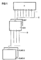
- FIG. 1 shows a part of a telephone exchange that belongs to its periphery.
- connection modules SLMO-0 to SLMO-3 are shown, to which subscriber lines are to be thought of.
- These line modules contain a corresponding number of subscriber sets, as well as a line group processor.
- connection modules mentioned are part of a larger plurality, which may be 128, for example.
- FIG. 1 also shows a central interface unit I1, via which the data is exchanged with the central parts of the switching center and via which the connection modules are supplied with clock pulses and synchronization signals.
- Distribution units BD0 to BD7 ensure a partially central distribution of data, clock and synchronization signals. They form an interface I2 on the input side and an interface I3 on the output side.
- the output 0 of the part of the interface I3 belonging to the distribution unit BD0 leads, as shown, to the connection modules SLMO-0 to SLMO-3 shown.
- the remaining outputs of this distribution unit or the outputs of the other distribution units lead to further connection modules, not shown here.
- connections of the illustrated distribution network may serve for the distribution of the clock pulse signals.
- Corresponding connections are to be considered for the transmission of the pulse frame signal and the data.
- the circuit according to the invention shown in FIG. 2, when used in an arrangement according to FIG. 1, is assigned to the outputs of the distribution units BD0 to BD7, to which it supplies interference-free clock pulses, from where only up to the connection modules SLMO-0 to SLMO-3 Cable connections of at most 60 cm have to be traversed, so that disruptive couplings can be avoided here without any special effort. If the clock signals arriving at the connection modules are nevertheless subject to interference, the circuit arrangement according to the invention can also be assigned to its inputs.
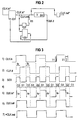
- the circuit arrangement according to the invention according to FIG. 2 has a blocking gate G1 to which the clock pulses, which may be subject to interference, are fed.
- a driver circuit G2 is connected to the output of this blocking gate G1, the output of which is fed back to the input via a resistor R1.
- the output of the blocking gate G1 is also connected to the input of a delay element V, the output of which is connected to the one input of a comparator G3, the other input of which is also connected to the output of the blocking gate G1.
- the output signal of the comparator G3 is fed to the blocking input X of the blocking gate G1.
- Holding circuit which is such that it immediately transfers a potential change at the start and end of the pulse to the output of the circuit arrangement in the form of a potential jump in the amount of the pulse amplitude, regardless of whether the input-side potential change leads to the pulse amplitude being reached or not, if only a threshold value is exceeded. After that, potential changes occurring at its input do not pass on until a certain period of time has elapsed. The time span is dimensioned such that any disturbances occurring at the start and end of the pulse have subsided after their start-up.
- the holding function could also be generated with the aid of a bistable flip-flop.
- line 1) shows a clock pulse sequence CLKin as it is fed to the blocking gate G1.
- the pulses are shown without interference, in the right part it is shown by way of example that the leading edge of a pulse is subject to interference in such a way that the signal does not yet reach the full amplitude when the edge changes after the pulse pause, and again the value before the edge falls back, see T1, i.e. is faulty and only assumes the correct value after a fault time.
- T2 shows a clock pulse sequence CLKin as it is fed to the blocking gate G1.
- the comparator G3 After the delay time, the comparator G3 signals equality again, so that the blocking gate is switched back to the active state and can thus react to an edge change again. Because of the time span, during the disturbances, persistent delay time will be the subsequent falling edge of the pulse.
- resistor R1 is dimensioned such that the potential CLKin * supplied by the now active blocking gate is compared to that occurring at the output of resistor R1 Potential CLKin # can enforce.
Applications Claiming Priority (2)
| Application Number | Priority Date | Filing Date | Title |
|---|---|---|---|
| DE4434084A DE4434084C1 (de) | 1994-09-23 | 1994-09-23 | Schaltungsanordnung zur Störbefreiung einer Taktsignalimpulsfolge |
| DE4434084 | 1994-09-23 |
Publications (2)
| Publication Number | Publication Date |
|---|---|
| EP0704787A1 true EP0704787A1 (fr) | 1996-04-03 |
| EP0704787B1 EP0704787B1 (fr) | 1997-11-12 |
Family
ID=6529052
Family Applications (1)
| Application Number | Title | Priority Date | Filing Date |
|---|---|---|---|
| EP95113633A Expired - Lifetime EP0704787B1 (fr) | 1994-09-23 | 1995-08-30 | Circuit pour l'élimination de parasites dans un train d'impulsions d'horloge |
Country Status (6)
| Country | Link |
|---|---|
| EP (1) | EP0704787B1 (fr) |
| AT (1) | ATE160231T1 (fr) |
| DE (2) | DE4434084C1 (fr) |
| DK (1) | DK0704787T3 (fr) |
| ES (1) | ES2109764T3 (fr) |
| GR (1) | GR3025434T3 (fr) |
Families Citing this family (1)
| Publication number | Priority date | Publication date | Assignee | Title |
|---|---|---|---|---|
| DE10164806B4 (de) * | 2000-09-29 | 2005-03-31 | Agilent Technologies, Inc. (n.d.Ges.d.Staates Delaware), Palo Alto | Polaritätsausblendverzögerungsschaltung zum Ausblenden von Ausgleichsvorgängen |
Citations (3)
| Publication number | Priority date | Publication date | Assignee | Title |
|---|---|---|---|---|
| EP0309849A1 (fr) * | 1987-09-28 | 1989-04-05 | Siemens Aktiengesellschaft | Arrangement de régénération des largeurs d'impulsion d'un signal numérique |
| US4988892A (en) * | 1989-06-02 | 1991-01-29 | Atari Corporation | Method and circuit for generating dependent clock signals |
| JPH03224020A (ja) * | 1990-01-30 | 1991-10-03 | Fujitsu Ltd | クロック受信回路 |
-
1994
- 1994-09-23 DE DE4434084A patent/DE4434084C1/de not_active Expired - Fee Related
-
1995
- 1995-08-30 EP EP95113633A patent/EP0704787B1/fr not_active Expired - Lifetime
- 1995-08-30 DK DK95113633T patent/DK0704787T3/da active
- 1995-08-30 ES ES95113633T patent/ES2109764T3/es not_active Expired - Lifetime
- 1995-08-30 AT AT95113633T patent/ATE160231T1/de not_active IP Right Cessation
- 1995-08-30 DE DE59500979T patent/DE59500979D1/de not_active Expired - Fee Related
-
1997
- 1997-11-19 GR GR970403079T patent/GR3025434T3/el unknown
Patent Citations (3)
| Publication number | Priority date | Publication date | Assignee | Title |
|---|---|---|---|---|
| EP0309849A1 (fr) * | 1987-09-28 | 1989-04-05 | Siemens Aktiengesellschaft | Arrangement de régénération des largeurs d'impulsion d'un signal numérique |
| US4988892A (en) * | 1989-06-02 | 1991-01-29 | Atari Corporation | Method and circuit for generating dependent clock signals |
| JPH03224020A (ja) * | 1990-01-30 | 1991-10-03 | Fujitsu Ltd | クロック受信回路 |
Non-Patent Citations (1)
| Title |
|---|
| PATENT ABSTRACTS OF JAPAN vol. 15, no. 515 (P - 1293) 27 December 1991 (1991-12-27) * |
Also Published As
| Publication number | Publication date |
|---|---|
| EP0704787B1 (fr) | 1997-11-12 |
| DE59500979D1 (de) | 1997-12-18 |
| ES2109764T3 (es) | 1998-01-16 |
| DK0704787T3 (da) | 1998-07-27 |
| GR3025434T3 (en) | 1998-02-27 |
| DE4434084C1 (de) | 1996-01-25 |
| ATE160231T1 (de) | 1997-11-15 |
Similar Documents
| Publication | Publication Date | Title |
|---|---|---|
| EP0275464B1 (fr) | Dispositif émetteur-récepteur pour un système à bus | |
| EP0269812A1 (fr) | Procédé et circuit pour l'alimentation d'une ligne d'horloge avec un signal d'horloge parmi deux en fonction du niveau d'un de ces deux signaux d'horloge | |
| DE3001397C2 (fr) | ||
| EP0235559B1 (fr) | Système de délivrance d'information pour la délivrance d'informations binaires | |
| EP0051141B1 (fr) | Procédé et dispositif pour l'égalisation de signaux binaires à la réception | |
| DE3442613C2 (fr) | ||
| DE3732287A1 (de) | Verfahren und schaltungsanordnung zum ableiten des worttaktes eines pulslagemodulierten signals | |
| DE19960785A1 (de) | Eingangsfilterstufe für einen Datenstrom und Verfahren zum Filtern eines Datenstroms | |
| DE2822835B2 (de) | Schaltungsanordnung zur Eliminierung koinzidenter Impulse | |
| EP0704787B1 (fr) | Circuit pour l'élimination de parasites dans un train d'impulsions d'horloge | |
| EP0977406B1 (fr) | Circuit de transmission de signaux numériques avec séparation galvanique | |
| EP0204376B1 (fr) | Circuit pour l'exploration d'un signal ternaire | |
| DE1199313B (de) | Schaltungsanordnung zum Wahrnehmen und Korrigieren von Datensignalverzerrungen | |
| DE2539804A1 (de) | Signalumsetzer, insbesondere vielfrequenzsignalempfaenger | |
| WO2001024441A2 (fr) | Procede et dispositif pour la communication bidirectionnelle entre au moins deux interlocuteurs | |
| DE3103574C2 (de) | Schaltungsanordnung zum Herstellen und Aufrechterhalten des Gleichlaufs zwischen von örtlich erzeugten Bittaktimpulsen abgeleiteten Envelopetaktimpulsen und in Envelopes eines binärcodierten Signals enthaltenen Synchronisierbits | |
| EP0063638B1 (fr) | Système de télécommunication numérique | |
| DE3401748A1 (de) | Schaltungsanordnung fuer eine digitale pegelregelung | |
| EP0234355B1 (fr) | Montage pour installations de télécommunication MIC, en particulier des centraux téléphoniques MIC avec plusieurs émetteurs synchrones commandés par impulsions d'horloge pour un canal d'émission commun | |
| EP0704786B1 (fr) | Circuit pour l'élimination de parasites dans un signal de trame | |
| EP0355607B1 (fr) | Circuit de synchronisation d'un signal numérique asynchrone à une horloge du système | |
| DE3205948A1 (de) | Datenkommunikationssystem | |
| DE1952549C3 (de) | Schaltungsanordnung zur Übertragung von Impulsen | |
| EP0384920B1 (fr) | Circuit pour régler d'une façon numérique dans un récepteur le gain d'un amplificateur | |
| DE4140920C1 (en) | Level changing circuitry for flanks of rectangular or trapezoidal signals - has threshold value discriminator with output signal separated into two channels, each having a gate circuit assigned to SR-flip=flop |
Legal Events
| Date | Code | Title | Description |
|---|---|---|---|
| PUAI | Public reference made under article 153(3) epc to a published international application that has entered the european phase |
Free format text: ORIGINAL CODE: 0009012 |
|
| AK | Designated contracting states |
Kind code of ref document: A1 Designated state(s): AT BE CH DE DK ES FR GB GR IE IT LI NL PT SE |
|
| 17P | Request for examination filed |
Effective date: 19960419 |
|
| GRAG | Despatch of communication of intention to grant |
Free format text: ORIGINAL CODE: EPIDOS AGRA |
|
| GRAH | Despatch of communication of intention to grant a patent |
Free format text: ORIGINAL CODE: EPIDOS IGRA |
|
| 17Q | First examination report despatched |
Effective date: 19970131 |
|
| GRAH | Despatch of communication of intention to grant a patent |
Free format text: ORIGINAL CODE: EPIDOS IGRA |
|
| GRAA | (expected) grant |
Free format text: ORIGINAL CODE: 0009210 |
|
| AK | Designated contracting states |
Kind code of ref document: B1 Designated state(s): AT BE CH DE DK ES FR GB GR IE IT LI NL PT SE |
|
| PG25 | Lapsed in a contracting state [announced via postgrant information from national office to epo] |
Ref country code: GR Free format text: LAPSE BECAUSE OF FAILURE TO SUBMIT A TRANSLATION OF THE DESCRIPTION OR TO PAY THE FEE WITHIN THE PRESCRIBED TIME-LIMIT Effective date: 19971112 |
|
| REF | Corresponds to: |
Ref document number: 160231 Country of ref document: AT Date of ref document: 19971115 Kind code of ref document: T |
|
| REG | Reference to a national code |
Ref country code: CH Ref legal event code: NV Representative=s name: SIEMENS SCHWEIZ AG Ref country code: CH Ref legal event code: EP |
|
| REF | Corresponds to: |
Ref document number: 59500979 Country of ref document: DE Date of ref document: 19971218 |
|
| ET | Fr: translation filed | ||
| REG | Reference to a national code |
Ref country code: ES Ref legal event code: FG2A Ref document number: 2109764 Country of ref document: ES Kind code of ref document: T3 |
|
| REG | Reference to a national code |
Ref country code: GR Ref legal event code: FG4A Free format text: 3025434 |
|
| GBT | Gb: translation of ep patent filed (gb section 77(6)(a)/1977) |
Effective date: 19980114 |
|
| ITF | It: translation for a ep patent filed |
Owner name: STUDIO JAUMANN P. & C. S.N.C. |
|
| REG | Reference to a national code |
Ref country code: PT Ref legal event code: SC4A Free format text: AVAILABILITY OF NATIONAL TRANSLATION Effective date: 19980209 |
|
| REG | Reference to a national code |
Ref country code: DK Ref legal event code: T3 |
|
| PG25 | Lapsed in a contracting state [announced via postgrant information from national office to epo] |
Ref country code: IE Free format text: LAPSE BECAUSE OF NON-PAYMENT OF DUE FEES Effective date: 19980830 Ref country code: DK Free format text: LAPSE BECAUSE OF NON-PAYMENT OF DUE FEES Effective date: 19980830 Ref country code: AT Free format text: LAPSE BECAUSE OF NON-PAYMENT OF DUE FEES Effective date: 19980830 |
|
| PG25 | Lapsed in a contracting state [announced via postgrant information from national office to epo] |
Ref country code: SE Free format text: LAPSE BECAUSE OF NON-PAYMENT OF DUE FEES Effective date: 19980831 Ref country code: ES Free format text: LAPSE BECAUSE OF NON-PAYMENT OF DUE FEES Effective date: 19980831 Ref country code: BE Free format text: LAPSE BECAUSE OF NON-PAYMENT OF DUE FEES Effective date: 19980831 |
|
| PLBE | No opposition filed within time limit |
Free format text: ORIGINAL CODE: 0009261 |
|
| STAA | Information on the status of an ep patent application or granted ep patent |
Free format text: STATUS: NO OPPOSITION FILED WITHIN TIME LIMIT |
|
| 26N | No opposition filed | ||
| BERE | Be: lapsed |
Owner name: SIEMENS A.G. Effective date: 19980831 |
|
| PG25 | Lapsed in a contracting state [announced via postgrant information from national office to epo] |
Ref country code: PT Free format text: LAPSE BECAUSE OF NON-PAYMENT OF DUE FEES Effective date: 19990228 |
|
| PG25 | Lapsed in a contracting state [announced via postgrant information from national office to epo] |
Ref country code: FR Free format text: LAPSE BECAUSE OF NON-PAYMENT OF DUE FEES Effective date: 19990430 |
|
| EUG | Se: european patent has lapsed |
Ref document number: 95113633.2 |
|
| PG25 | Lapsed in a contracting state [announced via postgrant information from national office to epo] |
Ref country code: DE Free format text: LAPSE BECAUSE OF NON-PAYMENT OF DUE FEES Effective date: 19990601 |
|
| REG | Reference to a national code |
Ref country code: FR Ref legal event code: ST |
|
| REG | Reference to a national code |
Ref country code: PT Ref legal event code: MM4A Free format text: LAPSE DUE TO NON-PAYMENT OF FEES Effective date: 19990228 |
|
| PG25 | Lapsed in a contracting state [announced via postgrant information from national office to epo] |
Ref country code: GB Free format text: LAPSE BECAUSE OF NON-PAYMENT OF DUE FEES Effective date: 19990830 |
|
| PG25 | Lapsed in a contracting state [announced via postgrant information from national office to epo] |
Ref country code: LI Free format text: LAPSE BECAUSE OF NON-PAYMENT OF DUE FEES Effective date: 19990831 Ref country code: CH Free format text: LAPSE BECAUSE OF NON-PAYMENT OF DUE FEES Effective date: 19990831 |
|
| PG25 | Lapsed in a contracting state [announced via postgrant information from national office to epo] |
Ref country code: NL Free format text: LAPSE BECAUSE OF NON-PAYMENT OF DUE FEES Effective date: 20000301 |
|
| REG | Reference to a national code |
Ref country code: CH Ref legal event code: PL |
|
| GBPC | Gb: european patent ceased through non-payment of renewal fee |
Effective date: 19990830 |
|
| NLV4 | Nl: lapsed or anulled due to non-payment of the annual fee |
Effective date: 20000301 |
|
| REG | Reference to a national code |
Ref country code: DK Ref legal event code: EBP |
|
| REG | Reference to a national code |
Ref country code: ES Ref legal event code: FD2A Effective date: 19990910 |
|
| PG25 | Lapsed in a contracting state [announced via postgrant information from national office to epo] |
Ref country code: IT Free format text: LAPSE BECAUSE OF NON-PAYMENT OF DUE FEES;WARNING: LAPSES OF ITALIAN PATENTS WITH EFFECTIVE DATE BEFORE 2007 MAY HAVE OCCURRED AT ANY TIME BEFORE 2007. THE CORRECT EFFECTIVE DATE MAY BE DIFFERENT FROM THE ONE RECORDED. Effective date: 20050830 |