EP0703667A1 - Circuit intégré de commande avec circuit de décalage de niveau pour la commutation d'un commutateur électronique - Google Patents
Circuit intégré de commande avec circuit de décalage de niveau pour la commutation d'un commutateur électronique Download PDFInfo
- Publication number
- EP0703667A1 EP0703667A1 EP94830436A EP94830436A EP0703667A1 EP 0703667 A1 EP0703667 A1 EP 0703667A1 EP 94830436 A EP94830436 A EP 94830436A EP 94830436 A EP94830436 A EP 94830436A EP 0703667 A1 EP0703667 A1 EP 0703667A1
- Authority
- EP
- European Patent Office
- Prior art keywords
- circuit
- resistor
- output
- transistors
- transistor
- Prior art date
- Legal status (The legal status is an assumption and is not a legal conclusion. Google has not performed a legal analysis and makes no representation as to the accuracy of the status listed.)
- Granted
Links
- 230000003071 parasitic effect Effects 0.000 claims abstract description 12
- 238000010586 diagram Methods 0.000 description 4
- 230000000694 effects Effects 0.000 description 3
- 239000003990 capacitor Substances 0.000 description 2
- 238000004519 manufacturing process Methods 0.000 description 2
- 238000000034 method Methods 0.000 description 2
- 238000004804 winding Methods 0.000 description 2
- 101150110971 CIN7 gene Proteins 0.000 description 1
- 101100286980 Daucus carota INV2 gene Proteins 0.000 description 1
- 101100508840 Daucus carota INV3 gene Proteins 0.000 description 1
- 101150110298 INV1 gene Proteins 0.000 description 1
- 101100397044 Xenopus laevis invs-a gene Proteins 0.000 description 1
- 101100397045 Xenopus laevis invs-b gene Proteins 0.000 description 1
- 230000008901 benefit Effects 0.000 description 1
- 230000000295 complement effect Effects 0.000 description 1
- 230000008878 coupling Effects 0.000 description 1
- 238000010168 coupling process Methods 0.000 description 1
- 238000005859 coupling reaction Methods 0.000 description 1
- 230000005669 field effect Effects 0.000 description 1
- 230000006870 function Effects 0.000 description 1
- 238000002347 injection Methods 0.000 description 1
- 239000007924 injection Substances 0.000 description 1
- 230000007257 malfunction Effects 0.000 description 1
- 230000008569 process Effects 0.000 description 1
- 239000000758 substrate Substances 0.000 description 1
- 230000007704 transition Effects 0.000 description 1
- 230000001960 triggered effect Effects 0.000 description 1
Images

Classifications
-
- H—ELECTRICITY
- H03—ELECTRONIC CIRCUITRY
- H03K—PULSE TECHNIQUE
- H03K17/00—Electronic switching or gating, i.e. not by contact-making and –breaking
- H03K17/51—Electronic switching or gating, i.e. not by contact-making and –breaking characterised by the components used
- H03K17/56—Electronic switching or gating, i.e. not by contact-making and –breaking characterised by the components used by the use, as active elements, of semiconductor devices
- H03K17/687—Electronic switching or gating, i.e. not by contact-making and –breaking characterised by the components used by the use, as active elements, of semiconductor devices the devices being field-effect transistors
-
- H—ELECTRICITY
- H03—ELECTRONIC CIRCUITRY
- H03K—PULSE TECHNIQUE
- H03K17/00—Electronic switching or gating, i.e. not by contact-making and –breaking
- H03K17/16—Modifications for eliminating interference voltages or currents
- H03K17/161—Modifications for eliminating interference voltages or currents in field-effect transistor switches
Definitions
- the present invention relates to switching control circuits for electronic power switches and, more particularly, to a circuit of this type including a control signal level shifter.
- One known application of electronic power switches is in forming bridge circuits for the actuation of motors. These circuits include pairs of electronic switches connected in series between the poles of a high voltage power supply. The load, in this case a winding of the motor, is connected between the connection points of the switches of the pairs. The switches of each pair are controlled in such a way that at any instant at most one of the two is closed. That is to say it cannot happen that both switches of a pair are simultaneously closed.
- the electronic switches are controlled by low voltage logic circuits which produce control signals at two levels referred to a reference voltage which, normally, is also the earth terminal of the circuit arrangement.
- a reference voltage which, normally, is also the earth terminal of the circuit arrangement.
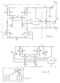
- a typical structure of a control circuit with a level shifter is schematically represented in Figure 1 of the attached drawings.
- Four power transistors for example field effect transistors (FET) of n channel DMOS type, indicated T1, T2, T3 and T4 are connected in series in pairs between the terminals, indicated with the earth symbol and V H , of a relatively high voltage DC power supply, for example 300 volts.
- a load L for example a winding of a motor not further shown, is connected between the connection nodes of the switches of the two pairs.
- a control logic circuit, indicated LG produces control signals at two voltage levels, for example the ground level, or zero, and a relatively low supply voltage level V LL , typically five volts.
- the driving circuit (DR2) of the transistor T2 is supplied with a relatively low voltage V L , for example 12 volts, sufficient to raise the gate electrode of T2 to a voltage, with respect to its source terminal (which is connected to ground) greater than the conduction threshold.
- the driving circuit DR1 of the transistor T1 is supplied with a voltage V C the value of which is substantially equal to V L provided by a "buffer" capacitor C connected between the connection node S1 (between the two transistors T1 and T2) and a charging circuit, not shown, the function of which is to maintain the capacitor C charged to the voltage V C .
- the level shifter LS1 includes two substantially identical circuit branches each constituted by an n channel MOS transistor M1, M2 the source terminal of which is connected to the ground terminal and the drain terminal of which is connected to the supply terminal V C via the parallel connection of a resistor R1, R2 and a zener diode D1, D2.
- the gate terminals of the transistors M1 and M2 are connected to an output of the logic circuit LG, one directly and the other through an inverter INV1, such that the control signals which arrive at the two transistors are always complementary to one another.
- the level shifter LS1 also includes a bistable (flip-flop) circuit, indicated RS, supplied with the voltage V C , and having "set” and “reset” terminals S, R respectively, connected via respective inverters INV2 and INV3 to the drain electrodes, respectively, of transistors M1 and M2, and an output terminal Q connected to the input of the driving circuit DR1 of transistor T1.
- RS bistable (flip-flop) circuit
- the two transistors M1 and M2 are alternatively brought to a conduction state by signals generated by the logic circuit LG.
- the current pulses which form in succession in the two resistors R1 and R2 produce the "set” and “reset” signals at the inputs S and R of the flip-flop RS and, consequently, the output signal Q from the flip-flop, which is referred to the voltage level of the node S1 (which varies substantially between 0 and V H in dependence on the state of conduction of the transistors of the bridge), causes the driving circuit DR1 to apply a voltage signal between the gate and source electrodes of the transistor T1, a voltage signal which switches on or off the transistor T1.
- circuit described above can be improved, in a manner which will be illustrated hereinbelow, to ensure that during switching of the node S1 between 0 and V H , both the inputs of the flip-flop are at low level.
- both the circuit of Figure 1 and the thus-improved circuit are subject, when forming part of a monolithic integrated circuit, to possible spurious switching such that they cannot be utilised when it is essential to achieve absolute security in operation of the transistor bridge.
- Spurious switching is due to the structure capacitances associated with the transistors M1 and M2.
- These capacitances are the sum of the capacitances between drain and source and between drain and substrate.
- the conduction of parasitic components is triggered due to the structure of the integrated circuit in which the various components of the switching control circuit are formed, which can lead to switching signals at the flip-flop which are not those caused by the control signal and which can therefore cause very serious malfunctions.
- the object of the present invention is to provide a switching control circuit with a level shifter for an electronic power switch in which spurious switching is not possible in any case.
- the two transistors Tp1 and Tp2 inject a current into the resistors R3 and R4. This takes place, in particular, in the switching phase of the node S1 from the higher level to the lower level when the power transistors T1 and T2 are, respectively, off and on.
- both the inputs of the flip-flop are at the higher level, that is to say in a state which does not in general correspond to a well defined output state of the flip-flop.
- the resistor R3, connected to the "reset” input (R) has a greater resistance than that of the resistor R4 connected to the "set” input (S).
- the layout of the integrated circuit is chosen in such a way that, during switching, the overall currents injected by the two parasitic current generators into one resistor and into the other resistor are not equal to one another but such that the overall current injected into the resistor connected to the "reset” input (R) is greater than that injected into the other resistor.
- the resistors R3 and R4 are equal, the level of the "set” terminal falls more rapidly than that of the "reset” terminal because the charge of the capacitance associated with the "set” terminal will be less than that of the capacitance associated with the "reset” terminal.
- One way of obtaining this result is to dispose the transistors M10 and M9 at a different distance from the centre of the areas in which the associated diodes D1 and D2 are formed. For example, as is shown in Figure 4, the distance d1 between M10 and the diodes D1 and D2 is greater than the distance d2 between M9 and the same pair of diodes. This exploits the fact that, with the usual fabrication processes for this type of integrated circuit, the gain of the parasitic pnp transistors Tp1, Tp2 is strongly influenced by these distances d1 and d2.
- the object of the invention is fully achieved in that the risk of spurious switching is entirely avoided. It is noted moreover that this effect is obtained without additional circuit components, but simply by dimensioning and/or suitably arranging some already existing components.
Landscapes
- Electronic Switches (AREA)
- Control Of Direct Current Motors (AREA)
- Logic Circuits (AREA)
Priority Applications (4)
| Application Number | Priority Date | Filing Date | Title |
|---|---|---|---|
| DE69403965T DE69403965T2 (de) | 1994-09-16 | 1994-09-16 | Integrierte Steuerschaltungsanordnung mit einem Pegelschieber zum Schalten eines elektronischen Schalters |
| EP94830436A EP0703667B1 (fr) | 1994-09-16 | 1994-09-16 | Circuit intégré de commande avec circuit de décalage de niveau pour la commutation d'un commutateur électronique |
| JP7214740A JP2642912B2 (ja) | 1994-09-16 | 1995-08-23 | 電子的スイッチのスイッチング用レベルシフタを有する集積形制御回路 |
| US08/529,882 US5552731A (en) | 1994-09-16 | 1995-09-18 | Integrated control circuit with a level shifter for switching an electronic switch |
Applications Claiming Priority (1)
| Application Number | Priority Date | Filing Date | Title |
|---|---|---|---|
| EP94830436A EP0703667B1 (fr) | 1994-09-16 | 1994-09-16 | Circuit intégré de commande avec circuit de décalage de niveau pour la commutation d'un commutateur électronique |
Publications (2)
| Publication Number | Publication Date |
|---|---|
| EP0703667A1 true EP0703667A1 (fr) | 1996-03-27 |
| EP0703667B1 EP0703667B1 (fr) | 1997-06-25 |
Family
ID=8218524
Family Applications (1)
| Application Number | Title | Priority Date | Filing Date |
|---|---|---|---|
| EP94830436A Expired - Lifetime EP0703667B1 (fr) | 1994-09-16 | 1994-09-16 | Circuit intégré de commande avec circuit de décalage de niveau pour la commutation d'un commutateur électronique |
Country Status (4)
| Country | Link |
|---|---|
| US (1) | US5552731A (fr) |
| EP (1) | EP0703667B1 (fr) |
| JP (1) | JP2642912B2 (fr) |
| DE (1) | DE69403965T2 (fr) |
Cited By (4)
| Publication number | Priority date | Publication date | Assignee | Title |
|---|---|---|---|---|
| WO2001075941A2 (fr) * | 2000-04-04 | 2001-10-11 | Koninklijke Philips Electronics N.V. | Circuit integre d'attaque en demi-pont a bas prix |
| WO2003050956A1 (fr) * | 2001-12-11 | 2003-06-19 | Koninklijke Philips Electronics N.V. | Dispositif de decalage de niveau haute tension par l'intermediaire de condensateurs |
| US8143831B2 (en) | 2006-04-05 | 2012-03-27 | Sitronic Ges. Fuer Elektrotechnische Ausruestung Mbh & Co. Kg | Regulating device for regulating the voltage on a high-side load |
| WO2014059317A1 (fr) * | 2012-10-11 | 2014-04-17 | Qualcomm Incorporated | Décaleur de niveau basse puissance compact pour doubles rails |
Families Citing this family (16)
| Publication number | Priority date | Publication date | Assignee | Title |
|---|---|---|---|---|
| WO1996032778A2 (fr) * | 1995-04-10 | 1996-10-17 | Philips Electronics N.V. | Circuit a decalage de niveau et circuit d'attaque cote tension haute integre |
| US5719521A (en) * | 1996-10-29 | 1998-02-17 | Philips Electronics North America Corporation | Integrated half-bridge timing control circuit |
| JP3635975B2 (ja) | 1999-03-02 | 2005-04-06 | 富士電機デバイステクノロジー株式会社 | レベルシフト回路 |
| US6362679B2 (en) * | 2000-02-23 | 2002-03-26 | Tripath Technology, Inc. | Power device driver circuit |
| JP4382312B2 (ja) * | 2001-09-05 | 2009-12-09 | 三菱電機株式会社 | 駆動制御装置、電力変換装置、電力変換装置の制御方法、および電力変換装置の使用方法 |
| DE10261433B3 (de) * | 2002-12-30 | 2004-08-19 | Infineon Technologies Ag | Schaltungsanordnung und Verfahren zur Ansteuerung eines in Reihe zu einer induktiven Last geschalteten Halbleiterschalters |
| US20050075809A1 (en) * | 2003-09-18 | 2005-04-07 | Ewc Controls Incorporated | Apparatus and method for detecting, filtering and conditioning AC voltage signals |
| DE102004060631A1 (de) * | 2003-12-16 | 2005-09-01 | International Rectifier Corp., El Segundo | Gate Treiber mit Pegelumsetzung zwischen statischen Wannen ohne Leistungsversorgung |
| US7126388B2 (en) * | 2004-12-16 | 2006-10-24 | Semiconductor Components Industries, L.L.C. | Power MOSFET driver and method therefor |
| US7843237B2 (en) * | 2008-11-17 | 2010-11-30 | Infineon Technologies Austria Ag | Circuit arrangement for actuating a transistor |
| JP5018866B2 (ja) * | 2009-11-19 | 2012-09-05 | サンケン電気株式会社 | レベルシフト回路及びスイッチング電源装置 |
| TWI446713B (zh) * | 2011-03-11 | 2014-07-21 | Richtek Technology Corp | 改良抗雜訊的浮接閘驅動器電路結構及其方法 |
| KR101350545B1 (ko) | 2012-05-31 | 2014-01-13 | 삼성전기주식회사 | 레벨 변환 회로 및 그를 포함하는 게이트 드라이버 회로 |
| JP6719242B2 (ja) * | 2016-03-23 | 2020-07-08 | エイブリック株式会社 | レベルシフト回路 |
| US10333408B1 (en) * | 2018-04-26 | 2019-06-25 | Dialog Semiconductor (Uk) Limited | Compensation of level-shift capacitance |
| CN110417242B (zh) * | 2018-06-08 | 2021-06-22 | 李湛明 | 用于GaN集成电路的高侧栅极驱动器 |
Citations (4)
| Publication number | Priority date | Publication date | Assignee | Title |
|---|---|---|---|---|
| EP0330628A2 (fr) * | 1988-02-25 | 1989-08-30 | STMicroelectronics S.r.l. | Circuit d'attaque MOS connecté du côté de l'alimentation |
| EP0397241A1 (fr) * | 1989-05-09 | 1990-11-14 | Koninklijke Philips Electronics N.V. | Excitateur pour circuits de demi-pont à tension élevée |
| US5105099A (en) * | 1991-03-01 | 1992-04-14 | Harris Corporation | Level shift circuit with common mode rejection |
| US5126603A (en) * | 1989-07-26 | 1992-06-30 | Nec Corporation | Circuit utilizes N-channel mos transistors having reduced area dimension for effectively detecting output current of a H-bridge circuit |
Family Cites Families (4)
| Publication number | Priority date | Publication date | Assignee | Title |
|---|---|---|---|---|
| US4677324A (en) * | 1986-03-21 | 1987-06-30 | Rca Corporation | Fast switch-off circuit for conductivity modulated field effect transistor |
| US4937468A (en) * | 1989-01-09 | 1990-06-26 | Sundstrand Corporation | Isolation circuit for pulse waveforms |
| FR2656965B1 (fr) * | 1990-01-09 | 1995-01-20 | Sgs Thomson Microelectronics | Commande et controle d'un commutateur de puissance. |
| US5365118A (en) * | 1992-06-04 | 1994-11-15 | Linear Technology Corp. | Circuit for driving two power mosfets in a half-bridge configuration |
-
1994
- 1994-09-16 DE DE69403965T patent/DE69403965T2/de not_active Expired - Fee Related
- 1994-09-16 EP EP94830436A patent/EP0703667B1/fr not_active Expired - Lifetime
-
1995
- 1995-08-23 JP JP7214740A patent/JP2642912B2/ja not_active Expired - Fee Related
- 1995-09-18 US US08/529,882 patent/US5552731A/en not_active Expired - Lifetime
Patent Citations (4)
| Publication number | Priority date | Publication date | Assignee | Title |
|---|---|---|---|---|
| EP0330628A2 (fr) * | 1988-02-25 | 1989-08-30 | STMicroelectronics S.r.l. | Circuit d'attaque MOS connecté du côté de l'alimentation |
| EP0397241A1 (fr) * | 1989-05-09 | 1990-11-14 | Koninklijke Philips Electronics N.V. | Excitateur pour circuits de demi-pont à tension élevée |
| US5126603A (en) * | 1989-07-26 | 1992-06-30 | Nec Corporation | Circuit utilizes N-channel mos transistors having reduced area dimension for effectively detecting output current of a H-bridge circuit |
| US5105099A (en) * | 1991-03-01 | 1992-04-14 | Harris Corporation | Level shift circuit with common mode rejection |
Non-Patent Citations (1)
| Title |
|---|
| ANON.: "Double circuit de commande pour MOSFET de puissance ou IGBT haute tension", ELECTRONIQUE APPLICATIONS, no. 63, December 1988 (1988-12-01), PARIS, FR., pages 33 - 38, XP000005008 * |
Cited By (6)
| Publication number | Priority date | Publication date | Assignee | Title |
|---|---|---|---|---|
| WO2001075941A2 (fr) * | 2000-04-04 | 2001-10-11 | Koninklijke Philips Electronics N.V. | Circuit integre d'attaque en demi-pont a bas prix |
| WO2001075941A3 (fr) * | 2000-04-04 | 2002-01-24 | Koninkl Philips Electronics Nv | Circuit integre d'attaque en demi-pont a bas prix |
| WO2003050956A1 (fr) * | 2001-12-11 | 2003-06-19 | Koninklijke Philips Electronics N.V. | Dispositif de decalage de niveau haute tension par l'intermediaire de condensateurs |
| US8143831B2 (en) | 2006-04-05 | 2012-03-27 | Sitronic Ges. Fuer Elektrotechnische Ausruestung Mbh & Co. Kg | Regulating device for regulating the voltage on a high-side load |
| WO2014059317A1 (fr) * | 2012-10-11 | 2014-04-17 | Qualcomm Incorporated | Décaleur de niveau basse puissance compact pour doubles rails |
| US9203411B2 (en) | 2012-10-11 | 2015-12-01 | Qualcomm Incorporated | Compact low power level shifter for dual rail |
Also Published As
| Publication number | Publication date |
|---|---|
| DE69403965D1 (de) | 1997-07-31 |
| EP0703667B1 (fr) | 1997-06-25 |
| JP2642912B2 (ja) | 1997-08-20 |
| DE69403965T2 (de) | 1998-01-29 |
| JPH08103098A (ja) | 1996-04-16 |
| US5552731A (en) | 1996-09-03 |
Similar Documents
| Publication | Publication Date | Title |
|---|---|---|
| EP0703666B1 (fr) | Circuit de commande avec circuit de décalage de niveau pour la commutation d'un commutateur électronique | |
| EP0703667B1 (fr) | Circuit intégré de commande avec circuit de décalage de niveau pour la commutation d'un commutateur électronique | |
| EP2164155B1 (fr) | Circuit de commande d'élément électronique | |
| US5818281A (en) | Semiconductor circuit having turn-on prevention capability of switching semiconductor device during off cycle thereof by undesired transient voltages | |
| US5818209A (en) | Bootstrap line power supply regulator with no filter capacitor | |
| US7535283B2 (en) | Gate drive circuit, semiconductor module and method for driving switching element | |
| US5963066A (en) | Semiconductor device which drives low-voltage driven switching device, using low-voltage direct current power source, a diode and a capacitor | |
| US5742196A (en) | Level-shifting circuit and high-side driver including such a level-shifting circuit | |
| US20030048116A1 (en) | Driving control device, power converting device, method of controlling power converting device and method of using power converting device | |
| KR970005567B1 (ko) | 단락 보호 회로 | |
| JP3702159B2 (ja) | 半導体集積回路装置 | |
| KR920009031B1 (ko) | 드라이버 회로 | |
| JPH11205123A (ja) | 高耐圧パワー集積回路 | |
| CN111030431B (zh) | 半导体装置 | |
| KR100639689B1 (ko) | 구동회로 | |
| JPH11205112A (ja) | 高耐圧パワー集積回路 | |
| US6683777B2 (en) | Semiconductor protective control unit for controlling output transistors connected to inductive load | |
| JP4727360B2 (ja) | 絶縁ゲート型半導体素子のゲート回路 | |
| JPH05252006A (ja) | 電力mosトランジスタを高電位側駆動構成において駆動するためのブートストラップ回路 | |
| JP3036423B2 (ja) | 半導体装置 | |
| JP4204119B2 (ja) | 誘導負荷をスイッチングするためのスイッチング装置 | |
| JPH09172358A (ja) | 高耐圧パワー集積回路 | |
| KR0133530B1 (ko) | 구동회로 | |
| JP3627605B2 (ja) | 電流制御型素子用駆動装置 | |
| JP3635953B2 (ja) | 高耐圧パワー集積回路 |
Legal Events
| Date | Code | Title | Description |
|---|---|---|---|
| PUAI | Public reference made under article 153(3) epc to a published international application that has entered the european phase |
Free format text: ORIGINAL CODE: 0009012 |
|
| 17P | Request for examination filed |
Effective date: 19950610 |
|
| AK | Designated contracting states |
Kind code of ref document: A1 Designated state(s): DE FR GB IT |
|
| GRAG | Despatch of communication of intention to grant |
Free format text: ORIGINAL CODE: EPIDOS AGRA |
|
| 17Q | First examination report despatched |
Effective date: 19960822 |
|
| GRAH | Despatch of communication of intention to grant a patent |
Free format text: ORIGINAL CODE: EPIDOS IGRA |
|
| GRAH | Despatch of communication of intention to grant a patent |
Free format text: ORIGINAL CODE: EPIDOS IGRA |
|
| GRAA | (expected) grant |
Free format text: ORIGINAL CODE: 0009210 |
|
| AK | Designated contracting states |
Kind code of ref document: B1 Designated state(s): DE FR GB IT |
|
| REF | Corresponds to: |
Ref document number: 69403965 Country of ref document: DE Date of ref document: 19970731 |
|
| ITF | It: translation for a ep patent filed | ||
| ET | Fr: translation filed | ||
| PLBE | No opposition filed within time limit |
Free format text: ORIGINAL CODE: 0009261 |
|
| STAA | Information on the status of an ep patent application or granted ep patent |
Free format text: STATUS: NO OPPOSITION FILED WITHIN TIME LIMIT |
|
| 26N | No opposition filed | ||
| REG | Reference to a national code |
Ref country code: GB Ref legal event code: IF02 |
|
| PGFP | Annual fee paid to national office [announced via postgrant information from national office to epo] |
Ref country code: DE Payment date: 20030925 Year of fee payment: 10 |
|
| PG25 | Lapsed in a contracting state [announced via postgrant information from national office to epo] |
Ref country code: DE Free format text: LAPSE BECAUSE OF NON-PAYMENT OF DUE FEES Effective date: 20050401 |
|
| PG25 | Lapsed in a contracting state [announced via postgrant information from national office to epo] |
Ref country code: IT Free format text: LAPSE BECAUSE OF NON-PAYMENT OF DUE FEES Effective date: 20050916 |
|
| PGFP | Annual fee paid to national office [announced via postgrant information from national office to epo] |
Ref country code: GB Payment date: 20060222 Year of fee payment: 12 |
|
| PGFP | Annual fee paid to national office [announced via postgrant information from national office to epo] |
Ref country code: FR Payment date: 20060227 Year of fee payment: 12 |
|
| GBPC | Gb: european patent ceased through non-payment of renewal fee |
Effective date: 20060916 |
|
| REG | Reference to a national code |
Ref country code: FR Ref legal event code: ST Effective date: 20070531 |
|
| PG25 | Lapsed in a contracting state [announced via postgrant information from national office to epo] |
Ref country code: GB Free format text: LAPSE BECAUSE OF NON-PAYMENT OF DUE FEES Effective date: 20060916 |
|
| PG25 | Lapsed in a contracting state [announced via postgrant information from national office to epo] |
Ref country code: FR Free format text: LAPSE BECAUSE OF NON-PAYMENT OF DUE FEES Effective date: 20061002 |