EP0703667A1 - An integrated control circuit with a level shifter for switching an electronic switch - Google Patents
An integrated control circuit with a level shifter for switching an electronic switch Download PDFInfo
- Publication number
- EP0703667A1 EP0703667A1 EP94830436A EP94830436A EP0703667A1 EP 0703667 A1 EP0703667 A1 EP 0703667A1 EP 94830436 A EP94830436 A EP 94830436A EP 94830436 A EP94830436 A EP 94830436A EP 0703667 A1 EP0703667 A1 EP 0703667A1
- Authority
- EP
- European Patent Office
- Prior art keywords
- circuit
- resistor
- output
- transistors
- transistor
- Prior art date
- Legal status (The legal status is an assumption and is not a legal conclusion. Google has not performed a legal analysis and makes no representation as to the accuracy of the status listed.)
- Granted
Links
Images

Classifications
-
- H—ELECTRICITY
- H03—ELECTRONIC CIRCUITRY
- H03K—PULSE TECHNIQUE
- H03K17/00—Electronic switching or gating, i.e. not by contact-making and –breaking
- H03K17/51—Electronic switching or gating, i.e. not by contact-making and –breaking characterised by the components used
- H03K17/56—Electronic switching or gating, i.e. not by contact-making and –breaking characterised by the components used by the use, as active elements, of semiconductor devices
- H03K17/687—Electronic switching or gating, i.e. not by contact-making and –breaking characterised by the components used by the use, as active elements, of semiconductor devices the devices being field-effect transistors
-
- H—ELECTRICITY
- H03—ELECTRONIC CIRCUITRY
- H03K—PULSE TECHNIQUE
- H03K17/00—Electronic switching or gating, i.e. not by contact-making and –breaking
- H03K17/16—Modifications for eliminating interference voltages or currents
- H03K17/161—Modifications for eliminating interference voltages or currents in field-effect transistor switches
Definitions
- the present invention relates to switching control circuits for electronic power switches and, more particularly, to a circuit of this type including a control signal level shifter.
- One known application of electronic power switches is in forming bridge circuits for the actuation of motors. These circuits include pairs of electronic switches connected in series between the poles of a high voltage power supply. The load, in this case a winding of the motor, is connected between the connection points of the switches of the pairs. The switches of each pair are controlled in such a way that at any instant at most one of the two is closed. That is to say it cannot happen that both switches of a pair are simultaneously closed.
- the electronic switches are controlled by low voltage logic circuits which produce control signals at two levels referred to a reference voltage which, normally, is also the earth terminal of the circuit arrangement.
- a reference voltage which, normally, is also the earth terminal of the circuit arrangement.
- a typical structure of a control circuit with a level shifter is schematically represented in Figure 1 of the attached drawings.
- Four power transistors for example field effect transistors (FET) of n channel DMOS type, indicated T1, T2, T3 and T4 are connected in series in pairs between the terminals, indicated with the earth symbol and V H , of a relatively high voltage DC power supply, for example 300 volts.
- a load L for example a winding of a motor not further shown, is connected between the connection nodes of the switches of the two pairs.
- a control logic circuit, indicated LG produces control signals at two voltage levels, for example the ground level, or zero, and a relatively low supply voltage level V LL , typically five volts.
- the driving circuit (DR2) of the transistor T2 is supplied with a relatively low voltage V L , for example 12 volts, sufficient to raise the gate electrode of T2 to a voltage, with respect to its source terminal (which is connected to ground) greater than the conduction threshold.
- the driving circuit DR1 of the transistor T1 is supplied with a voltage V C the value of which is substantially equal to V L provided by a "buffer" capacitor C connected between the connection node S1 (between the two transistors T1 and T2) and a charging circuit, not shown, the function of which is to maintain the capacitor C charged to the voltage V C .
- the level shifter LS1 includes two substantially identical circuit branches each constituted by an n channel MOS transistor M1, M2 the source terminal of which is connected to the ground terminal and the drain terminal of which is connected to the supply terminal V C via the parallel connection of a resistor R1, R2 and a zener diode D1, D2.
- the gate terminals of the transistors M1 and M2 are connected to an output of the logic circuit LG, one directly and the other through an inverter INV1, such that the control signals which arrive at the two transistors are always complementary to one another.
- the level shifter LS1 also includes a bistable (flip-flop) circuit, indicated RS, supplied with the voltage V C , and having "set” and “reset” terminals S, R respectively, connected via respective inverters INV2 and INV3 to the drain electrodes, respectively, of transistors M1 and M2, and an output terminal Q connected to the input of the driving circuit DR1 of transistor T1.
- RS bistable (flip-flop) circuit
- the two transistors M1 and M2 are alternatively brought to a conduction state by signals generated by the logic circuit LG.
- the current pulses which form in succession in the two resistors R1 and R2 produce the "set” and “reset” signals at the inputs S and R of the flip-flop RS and, consequently, the output signal Q from the flip-flop, which is referred to the voltage level of the node S1 (which varies substantially between 0 and V H in dependence on the state of conduction of the transistors of the bridge), causes the driving circuit DR1 to apply a voltage signal between the gate and source electrodes of the transistor T1, a voltage signal which switches on or off the transistor T1.
- circuit described above can be improved, in a manner which will be illustrated hereinbelow, to ensure that during switching of the node S1 between 0 and V H , both the inputs of the flip-flop are at low level.
- both the circuit of Figure 1 and the thus-improved circuit are subject, when forming part of a monolithic integrated circuit, to possible spurious switching such that they cannot be utilised when it is essential to achieve absolute security in operation of the transistor bridge.
- Spurious switching is due to the structure capacitances associated with the transistors M1 and M2.
- These capacitances are the sum of the capacitances between drain and source and between drain and substrate.
- the conduction of parasitic components is triggered due to the structure of the integrated circuit in which the various components of the switching control circuit are formed, which can lead to switching signals at the flip-flop which are not those caused by the control signal and which can therefore cause very serious malfunctions.
- the object of the present invention is to provide a switching control circuit with a level shifter for an electronic power switch in which spurious switching is not possible in any case.
- the two transistors Tp1 and Tp2 inject a current into the resistors R3 and R4. This takes place, in particular, in the switching phase of the node S1 from the higher level to the lower level when the power transistors T1 and T2 are, respectively, off and on.
- both the inputs of the flip-flop are at the higher level, that is to say in a state which does not in general correspond to a well defined output state of the flip-flop.
- the resistor R3, connected to the "reset” input (R) has a greater resistance than that of the resistor R4 connected to the "set” input (S).
- the layout of the integrated circuit is chosen in such a way that, during switching, the overall currents injected by the two parasitic current generators into one resistor and into the other resistor are not equal to one another but such that the overall current injected into the resistor connected to the "reset” input (R) is greater than that injected into the other resistor.
- the resistors R3 and R4 are equal, the level of the "set” terminal falls more rapidly than that of the "reset” terminal because the charge of the capacitance associated with the "set” terminal will be less than that of the capacitance associated with the "reset” terminal.
- One way of obtaining this result is to dispose the transistors M10 and M9 at a different distance from the centre of the areas in which the associated diodes D1 and D2 are formed. For example, as is shown in Figure 4, the distance d1 between M10 and the diodes D1 and D2 is greater than the distance d2 between M9 and the same pair of diodes. This exploits the fact that, with the usual fabrication processes for this type of integrated circuit, the gain of the parasitic pnp transistors Tp1, Tp2 is strongly influenced by these distances d1 and d2.
- the object of the invention is fully achieved in that the risk of spurious switching is entirely avoided. It is noted moreover that this effect is obtained without additional circuit components, but simply by dimensioning and/or suitably arranging some already existing components.
Abstract
Description
- The present invention relates to switching control circuits for electronic power switches and, more particularly, to a circuit of this type including a control signal level shifter.
- One known application of electronic power switches is in forming bridge circuits for the actuation of motors. These circuits include pairs of electronic switches connected in series between the poles of a high voltage power supply. The load, in this case a winding of the motor, is connected between the connection points of the switches of the pairs. The switches of each pair are controlled in such a way that at any instant at most one of the two is closed. That is to say it cannot happen that both switches of a pair are simultaneously closed.
- The electronic switches are controlled by low voltage logic circuits which produce control signals at two levels referred to a reference voltage which, normally, is also the earth terminal of the circuit arrangement. For controlling the switches of the bridge connected to the positive pole of the power supply the level of the logic circuit signals is shifted by means of suitable level shifter circuits.
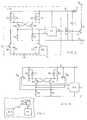
- A typical structure of a control circuit with a level shifter is schematically represented in Figure 1 of the attached drawings. Four power transistors, for example field effect transistors (FET) of n channel DMOS type, indicated T1, T2, T3 and T4 are connected in series in pairs between the terminals, indicated with the earth symbol and VH, of a relatively high voltage DC power supply, for example 300 volts. A load L, for example a winding of a motor not further shown, is connected between the connection nodes of the switches of the two pairs. A control logic circuit, indicated LG, produces control signals at two voltage levels, for example the ground level, or zero, and a relatively low supply voltage level VLL, typically five volts. These signals, available on the outputs of the logic circuit LG are applied to the control terminals, that is to say the gate electrodes both of the "lower" transistors T2, T4 through respective driving circuits, and the "upper" transistors T1, T3, through respective level shifting and driving circuits, to switch the transistors on or off (conduction or cut-off) according to the sequence determined by the logic circuit LG. For simplicity of the drawing only the driving circuits DR1 and DR2 for the transistors T1 and T2 and only the level shifter LS1 relating to the transistor T1 are shown; it is understood that similar circuits are provided for control of the transistors T3 and T4.
- The driving circuit (DR2) of the transistor T2 is supplied with a relatively low voltage VL, for example 12 volts, sufficient to raise the gate electrode of T2 to a voltage, with respect to its source terminal (which is connected to ground) greater than the conduction threshold. The driving circuit DR1 of the transistor T1 is supplied with a voltage VC the value of which is substantially equal to VL provided by a "buffer" capacitor C connected between the connection node S1 (between the two transistors T1 and T2) and a charging circuit, not shown, the function of which is to maintain the capacitor C charged to the voltage VC.
- The level shifter LS1 includes two substantially identical circuit branches each constituted by an n channel MOS transistor M1, M2 the source terminal of which is connected to the ground terminal and the drain terminal of which is connected to the supply terminal VC via the parallel connection of a resistor R1, R2 and a zener diode D1, D2. The gate terminals of the transistors M1 and M2 are connected to an output of the logic circuit LG, one directly and the other through an inverter INV1, such that the control signals which arrive at the two transistors are always complementary to one another.
- The level shifter LS1 also includes a bistable (flip-flop) circuit, indicated RS, supplied with the voltage VC, and having "set" and "reset" terminals S, R respectively, connected via respective inverters INV2 and INV3 to the drain electrodes, respectively, of transistors M1 and M2, and an output terminal Q connected to the input of the driving circuit DR1 of transistor T1.
- In operation the two transistors M1 and M2 are alternatively brought to a conduction state by signals generated by the logic circuit LG. The current pulses which form in succession in the two resistors R1 and R2 produce the "set" and "reset" signals at the inputs S and R of the flip-flop RS and, consequently, the output signal Q from the flip-flop, which is referred to the voltage level of the node S1 (which varies substantially between 0 and VH in dependence on the state of conduction of the transistors of the bridge), causes the driving circuit DR1 to apply a voltage signal between the gate and source electrodes of the transistor T1, a voltage signal which switches on or off the transistor T1.
- The circuit described above can be improved, in a manner which will be illustrated hereinbelow, to ensure that during switching of the node S1 between 0 and VH, both the inputs of the flip-flop are at low level. However, both the circuit of Figure 1 and the thus-improved circuit are subject, when forming part of a monolithic integrated circuit, to possible spurious switching such that they cannot be utilised when it is essential to achieve absolute security in operation of the transistor bridge.
- Spurious switching is due to the structure capacitances associated with the transistors M1 and M2. These capacitances, generally indicated C1 and C2 in Figure 1, are the sum of the capacitances between drain and source and between drain and substrate. In certain conditions, as will be explained in more detail hereinbelow in relation to a particular circuit, during discharge of these capacitances, which takes place in part through the zener diodes, D1 and D2 and in part through the resistors R1 and R2, the conduction of parasitic components is triggered due to the structure of the integrated circuit in which the various components of the switching control circuit are formed, which can lead to switching signals at the flip-flop which are not those caused by the control signal and which can therefore cause very serious malfunctions.
- The object of the present invention is to provide a switching control circuit with a level shifter for an electronic power switch in which spurious switching is not possible in any case.
- This object is achieved according to the invention by a circuit as defined and characterised in general in the first and second of the claims which follow the present description.
- The invention will be better understood from the following detailed description of an exemplary, and therefore non-limitative embodiment in relation to the attached drawings, in which:
- Figure 1, already described, is a diagram of a known switching control circuit applied to a transistor bridge;
- Figure 2 is a diagram of a switching control circuit to which the invention is applied;
- Figure 3 is a detail of the diagram of Figure 2 in which parasitic components not shown in Figure 2 are indicated; and
- Figure 4 schematically shows the relative arrangement of some components of the integrated circuit.
- The circuit of Figure 2, in which parts which are the same as or correspond to those of Figure 1 are indicated with the same reference symbols, is different from that of Figure 1 substantially in that the input terminals S and R of the flip-flop RS are not connected to the drain electrodes of the transistors M1 and M2 through inverters, but through a coupling stage which comprises two p channel MOSFETs, indicated M9 and M10. These are each connected with a respective series resistor R3 and R4 between the drains of the transistors M2 and M1 and the node S1, and have their gate electrodes connected to the source electrode of the other transistor of the pair.
- The current injected alternately into the resistors R1 and R2 during conduction of the transistors M1 and M2 respectively, causes conduction of the transistors M9 or M10 respectively such that across the resistors R3 or R4 there is a voltage drop which gives rise to the "reset" or "set" signals on the flip-flop RS. This circuit offers the advantage over the circuit of Figure 1 of maintaining the condition of low level signals S=0, R=0 on both inputs of the flip-flop during switching of the node S1. This is important in particular when the node S1 switches to a high voltage level, that is to say varies from 0 to VH.
- However, discharge of the capacitances C1 and C2 can cause spurious signals. In particular, if the circuit of Figure 2 is made as an integrated circuit using the usual fabrication techniques, parasitic bipolar transistors of pnp type are formed which constitute parasitic current generators associated with the p channel MOSFET transistors M10 and M9, and the effect of which can be evaluated by examining the equivalent diagram of Figure 3. As is seen, this shows two double collector transistors indicated Tp1 and Tp2, each having its emitter region in common with the source region of a respective p channel MOSFET transistor M10 and M9, its base region connected to the supply terminal VC and two collector regions in common with the drain regions of M10 and M9 connected to the input terminals S and R of the flip-flop. In the discharge phase of the capacitances C1 and C2 the two transistors Tp1 and Tp2 inject a current into the resistors R3 and R4. This takes place, in particular, in the switching phase of the node S1 from the higher level to the lower level when the power transistors T1 and T2 are, respectively, off and on. In this phase both the inputs of the flip-flop are at the higher level, that is to say in a state which does not in general correspond to a well defined output state of the flip-flop. To prevent this condition from causing an output of the flip-flop corresponding to a switching on of the power transistor T1, it is advisable to utilise a flip-flop of the "dominant reset" type, that is to say which has a low output level when the inputs are both at high level. However, even in this case, at the end of the transition of the node S1 from VH to 0 with the transistor T1 in the cut-off state, there is the risk that the flip-flop will enter the input condition which would take the transistor T1 back into conduction during the conduction of the lower transistor T2, this situation being highly undesirable. In fact, the voltage levels on the inputs S and R of the flip-flop, once the parasitic injection has ceased, tend to fall to the level of the node S1 gradually so that the capacitances associated with the two terminals S and R discharge through the resistors R4 and R3 until the so-called memory state (S=O, R=O) of the flip-flop is reached. In this condition the output state Q will be determined by that of the two levels which falls fastest. For example, in the case of a more rapid fall of the input R there would be the unwanted condition S=1, R=0 which would take the power transistor T1 into conduction.
- According to the invention, in order to prevent this from happening the resistor R3, connected to the "reset" input (R) has a greater resistance than that of the resistor R4 connected to the "set" input (S). Thus, with the same charge injected by the parasitic generators into the resistors R3 and R4, the level of the "set" terminal falls more rapidly than that of the "reset" terminal by the effect of the smaller time constant, so that at the end the output Q always corresponds to the state S=0, R=1.
- In another embodiment of the invention the layout of the integrated circuit, that is to say the arrangement of the circuit components, is chosen in such a way that, during switching, the overall currents injected by the two parasitic current generators into one resistor and into the other resistor are not equal to one another but such that the overall current injected into the resistor connected to the "reset" input (R) is greater than that injected into the other resistor. In this case, even if the resistors R3 and R4 are equal, the level of the "set" terminal falls more rapidly than that of the "reset" terminal because the charge of the capacitance associated with the "set" terminal will be less than that of the capacitance associated with the "reset" terminal.
- One way of obtaining this result is to dispose the transistors M10 and M9 at a different distance from the centre of the areas in which the associated diodes D1 and D2 are formed. For example, as is shown in Figure 4, the distance d1 between M10 and the diodes D1 and D2 is greater than the distance d2 between M9 and the same pair of diodes. This exploits the fact that, with the usual fabrication processes for this type of integrated circuit, the gain of the parasitic pnp transistors Tp1, Tp2 is strongly influenced by these distances d1 and d2.
- Naturally, the two above-described arrangements, that is to say that relating to the dimensioning of the two resistors R3 and R4 and the topological arrangement relating to the mutual disposition of the transistors M10, M9 and the diodes D1 and D2, can be utilised contemporaneously thus increasing the security of operation of the circuit.
- As can be easily established, the object of the invention is fully achieved in that the risk of spurious switching is entirely avoided. It is noted moreover that this effect is obtained without additional circuit components, but simply by dimensioning and/or suitably arranging some already existing components.
Claims (3)
- An integrated control circuit for switching an electronic power switch (T1) connected in series with a load (L) between first and second supply terminals (ground, VH) comprising
a control logic circuit (LG) adapted to produce an output signal having two voltage levels referred to the voltage level of a reference terminal (ground),
a level shift circuit (LS1) the input of which is connected to the output of the control logic circuit (LG) and an output of which is connected to the control terminal of the electronic switch (T1), and adapted to produce at its output a signal having two voltage levels, corresponding to the signals from the control logic circuit, referred to the voltage level of the connection node (S1) between the electronic switch (T1) and the load (L),
this level shift circuit (LS1) comprising
a bistable stage (RS) having a "set" input (S), a "reset" input (R) and an output (Q) which is the output from the level shift circuit,
first and second circuit branches connected between the said connection node (S1) and a third supply terminal (VC), respectively comprising a first transistor (M10) and a second transistor (M9) connected to the control logic circuit (LG) to be switched alternatively, a first resistor (R4) and a second resistor (R3) connected between the connection node (S1) and, respectively, the first transistor (M10) and the second transistor (M9), the first resistor (R4) being connected to the "set" input (S) and the second resistor (R3) being connected to the "reset" input (R) of the bistable stage (RS),
and first and second parasitic current generators (Tp1, Tp2), respectively associated with the first and second transistors (M10, M9) and adapted to inject current into the first and second resistors (R4, R3) respectively,
characterized in that the first resistor (R4) has a smaller resistance than that of the second resistor (R3). - An integrated circuit for controlling the switching of an electronic power switch (T1) connected in series with a load (L) between first and second supply terminals (ground, VH) comprising:
a control logic circuit (LG) adapted to produce an output signal at two voltage levels referred to the voltage level of a reference terminal (ground),
a level shift circuit (LS1) the input of which is connected to the output of the control logic circuit (LG) and the output of which is connected to the control terminal of the electronic switch (T1) and which is adapted to produce at its output a signal at two voltage levels corresponding to the control logic circuit signal, referred to the voltage level of the connection node (S1) between the electronic switch (T1) and the load (L), this level shift circuit (LS1) comprising
a bistable stage (RS) having a "set" input (S), a "reset" input (R) and an output (Q) which is the output from the level shift circuit,
first and second circuit branches connected between the said connection node (S1) and a third supply terminal (VC), respectively comprising first and second transistors (M10, M9) connected to the control logic circuit (LG) to be switched alternatively, first and second resistors (R4, R3) connected between the connection node (S1) and the first and second transistor (M10, M9) respectively, the first resistor (R4) being connected to the "set" input (S) and the second resistor (R3) being connected to the "reset" input (R) of the bistable stage (RS),
and first and second (Tp1, Tp2) parasitic current generators, associated, respectively, with the first transistor (M10) and the second transistor (M9) and adapted to inject current into the first resistor (R4) and the second resistor (R3),
characterized in that the arrangement of circuit components is chosen in such a way that the overall current injected, during switching, by the first and second current generators, (Tp1, Tp2) into the second resistor (R3) is greater than that injected by the same generators into the first resistor (R4). - An integrated circuit according to Claim 2, in which the first and second transistors (M10, M9) are p channel MOSFET transistors the drain terminals of which are connected to the first and second resistors (R4, R3) respectively, in which the first and second circuit branches include respective first and second diodes (D1, D2) connected between the source terminals of the first and second transistors (M10, M9) respectively and the third supply terminal (VC), and in which the first and second current generators are parasitic bipolar transistors (Tp1, Tp2) of pnp type having their emitter regions in common with the respective source region of the first and second transistors (M10, M9), a base region connected to the third supply terminal (VC), and each having two collector regions which are in common with respective drain regions of the first and second transistors (M10, M9), the first transistor (M10) being formed in an integrated circuit zone which is located at a distance from the centre of the zones in which the first and second diodes (D1, D2) are formed which is greater than the distance between the zone in which the second transistor (M9) is formed and the centre itself.
Priority Applications (4)
| Application Number | Priority Date | Filing Date | Title |
|---|---|---|---|
| EP94830436A EP0703667B1 (en) | 1994-09-16 | 1994-09-16 | An integrated control circuit with a level shifter for switching an electronic switch |
| DE69403965T DE69403965T2 (en) | 1994-09-16 | 1994-09-16 | Integrated control circuit arrangement with a level shifter for switching an electronic switch |
| JP7214740A JP2642912B2 (en) | 1994-09-16 | 1995-08-23 | Integrated control circuit with level shifter for switching electronic switches |
| US08/529,882 US5552731A (en) | 1994-09-16 | 1995-09-18 | Integrated control circuit with a level shifter for switching an electronic switch |
Applications Claiming Priority (1)
| Application Number | Priority Date | Filing Date | Title |
|---|---|---|---|
| EP94830436A EP0703667B1 (en) | 1994-09-16 | 1994-09-16 | An integrated control circuit with a level shifter for switching an electronic switch |
Publications (2)
| Publication Number | Publication Date |
|---|---|
| EP0703667A1 true EP0703667A1 (en) | 1996-03-27 |
| EP0703667B1 EP0703667B1 (en) | 1997-06-25 |
Family
ID=8218524
Family Applications (1)
| Application Number | Title | Priority Date | Filing Date |
|---|---|---|---|
| EP94830436A Expired - Lifetime EP0703667B1 (en) | 1994-09-16 | 1994-09-16 | An integrated control circuit with a level shifter for switching an electronic switch |
Country Status (4)
| Country | Link |
|---|---|
| US (1) | US5552731A (en) |
| EP (1) | EP0703667B1 (en) |
| JP (1) | JP2642912B2 (en) |
| DE (1) | DE69403965T2 (en) |
Cited By (4)
| Publication number | Priority date | Publication date | Assignee | Title |
|---|---|---|---|---|
| WO2001075941A2 (en) * | 2000-04-04 | 2001-10-11 | Koninklijke Philips Electronics N.V. | A low cost half bridge driver integrated circuit |
| WO2003050956A1 (en) * | 2001-12-11 | 2003-06-19 | Koninklijke Philips Electronics N.V. | High-voltage level shifter via capacitors |
| US8143831B2 (en) | 2006-04-05 | 2012-03-27 | Sitronic Ges. Fuer Elektrotechnische Ausruestung Mbh & Co. Kg | Regulating device for regulating the voltage on a high-side load |
| WO2014059317A1 (en) * | 2012-10-11 | 2014-04-17 | Qualcomm Incorporated | A compact low power level shifter for dual rail |
Families Citing this family (16)
| Publication number | Priority date | Publication date | Assignee | Title |
|---|---|---|---|---|
| EP0764365A2 (en) * | 1995-04-10 | 1997-03-26 | Koninklijke Philips Electronics N.V. | Level-shifting circuit and high-side driver including such a level-shifting circuit |
| US5719521A (en) * | 1996-10-29 | 1998-02-17 | Philips Electronics North America Corporation | Integrated half-bridge timing control circuit |
| JP3635975B2 (en) | 1999-03-02 | 2005-04-06 | 富士電機デバイステクノロジー株式会社 | Level shift circuit |
| US6362679B2 (en) * | 2000-02-23 | 2002-03-26 | Tripath Technology, Inc. | Power device driver circuit |
| JP4382312B2 (en) * | 2001-09-05 | 2009-12-09 | 三菱電機株式会社 | Drive control device, power conversion device, power conversion device control method, and power conversion device use method |
| DE10261433B3 (en) * | 2002-12-30 | 2004-08-19 | Infineon Technologies Ag | Control circuit for semiconductor switch in series with inductive load provides two alternate control signals dependent on comparison between input signal value and voltage measuring signal |
| US20050075809A1 (en) * | 2003-09-18 | 2005-04-07 | Ewc Controls Incorporated | Apparatus and method for detecting, filtering and conditioning AC voltage signals |
| CN100355207C (en) * | 2003-12-16 | 2007-12-12 | 国际整流器公司 | Gate driver with level shift between static wells with no power supply |
| US7126388B2 (en) * | 2004-12-16 | 2006-10-24 | Semiconductor Components Industries, L.L.C. | Power MOSFET driver and method therefor |
| US7843237B2 (en) * | 2008-11-17 | 2010-11-30 | Infineon Technologies Austria Ag | Circuit arrangement for actuating a transistor |
| JP5018866B2 (en) * | 2009-11-19 | 2012-09-05 | サンケン電気株式会社 | Level shift circuit and switching power supply device |
| TWI446713B (en) * | 2011-03-11 | 2014-07-21 | Richtek Technology Corp | Improved noise immunity floating gate driver circuit configuration and method thereof |
| KR101350545B1 (en) | 2012-05-31 | 2014-01-13 | 삼성전기주식회사 | Level shifter circuit and gate driver circuit including the same |
| JP6719242B2 (en) * | 2016-03-23 | 2020-07-08 | エイブリック株式会社 | Level shift circuit |
| US10333408B1 (en) * | 2018-04-26 | 2019-06-25 | Dialog Semiconductor (Uk) Limited | Compensation of level-shift capacitance |
| CN110417242B (en) * | 2018-06-08 | 2021-06-22 | 李湛明 | High side gate driver for GaN integrated circuits |
Citations (4)
| Publication number | Priority date | Publication date | Assignee | Title |
|---|---|---|---|---|
| EP0330628A2 (en) * | 1988-02-25 | 1989-08-30 | STMicroelectronics S.r.l. | High side driver MOS circuit |
| EP0397241A1 (en) * | 1989-05-09 | 1990-11-14 | Koninklijke Philips Electronics N.V. | Driver for high voltage half-bridge circuits |
| US5105099A (en) * | 1991-03-01 | 1992-04-14 | Harris Corporation | Level shift circuit with common mode rejection |
| US5126603A (en) * | 1989-07-26 | 1992-06-30 | Nec Corporation | Circuit utilizes N-channel mos transistors having reduced area dimension for effectively detecting output current of a H-bridge circuit |
Family Cites Families (4)
| Publication number | Priority date | Publication date | Assignee | Title |
|---|---|---|---|---|
| US4677324A (en) * | 1986-03-21 | 1987-06-30 | Rca Corporation | Fast switch-off circuit for conductivity modulated field effect transistor |
| US4937468A (en) * | 1989-01-09 | 1990-06-26 | Sundstrand Corporation | Isolation circuit for pulse waveforms |
| FR2656965B1 (en) * | 1990-01-09 | 1995-01-20 | Sgs Thomson Microelectronics | COMMAND AND CONTROL OF A POWER SWITCH. |
| US5365118A (en) * | 1992-06-04 | 1994-11-15 | Linear Technology Corp. | Circuit for driving two power mosfets in a half-bridge configuration |
-
1994
- 1994-09-16 DE DE69403965T patent/DE69403965T2/en not_active Expired - Fee Related
- 1994-09-16 EP EP94830436A patent/EP0703667B1/en not_active Expired - Lifetime
-
1995
- 1995-08-23 JP JP7214740A patent/JP2642912B2/en not_active Expired - Fee Related
- 1995-09-18 US US08/529,882 patent/US5552731A/en not_active Expired - Lifetime
Patent Citations (4)
| Publication number | Priority date | Publication date | Assignee | Title |
|---|---|---|---|---|
| EP0330628A2 (en) * | 1988-02-25 | 1989-08-30 | STMicroelectronics S.r.l. | High side driver MOS circuit |
| EP0397241A1 (en) * | 1989-05-09 | 1990-11-14 | Koninklijke Philips Electronics N.V. | Driver for high voltage half-bridge circuits |
| US5126603A (en) * | 1989-07-26 | 1992-06-30 | Nec Corporation | Circuit utilizes N-channel mos transistors having reduced area dimension for effectively detecting output current of a H-bridge circuit |
| US5105099A (en) * | 1991-03-01 | 1992-04-14 | Harris Corporation | Level shift circuit with common mode rejection |
Non-Patent Citations (1)
| Title |
|---|
| ANON.: "Double circuit de commande pour MOSFET de puissance ou IGBT haute tension", ELECTRONIQUE APPLICATIONS, no. 63, December 1988 (1988-12-01), PARIS, FR., pages 33 - 38, XP000005008 * |
Cited By (6)
| Publication number | Priority date | Publication date | Assignee | Title |
|---|---|---|---|---|
| WO2001075941A2 (en) * | 2000-04-04 | 2001-10-11 | Koninklijke Philips Electronics N.V. | A low cost half bridge driver integrated circuit |
| WO2001075941A3 (en) * | 2000-04-04 | 2002-01-24 | Koninkl Philips Electronics Nv | A low cost half bridge driver integrated circuit |
| WO2003050956A1 (en) * | 2001-12-11 | 2003-06-19 | Koninklijke Philips Electronics N.V. | High-voltage level shifter via capacitors |
| US8143831B2 (en) | 2006-04-05 | 2012-03-27 | Sitronic Ges. Fuer Elektrotechnische Ausruestung Mbh & Co. Kg | Regulating device for regulating the voltage on a high-side load |
| WO2014059317A1 (en) * | 2012-10-11 | 2014-04-17 | Qualcomm Incorporated | A compact low power level shifter for dual rail |
| US9203411B2 (en) | 2012-10-11 | 2015-12-01 | Qualcomm Incorporated | Compact low power level shifter for dual rail |
Also Published As
| Publication number | Publication date |
|---|---|
| EP0703667B1 (en) | 1997-06-25 |
| DE69403965T2 (en) | 1998-01-29 |
| US5552731A (en) | 1996-09-03 |
| DE69403965D1 (en) | 1997-07-31 |
| JPH08103098A (en) | 1996-04-16 |
| JP2642912B2 (en) | 1997-08-20 |
Similar Documents
| Publication | Publication Date | Title |
|---|---|---|
| EP0703666B1 (en) | A control circuit with a level shifter for switching an electronic switch | |
| EP0703667B1 (en) | An integrated control circuit with a level shifter for switching an electronic switch | |
| EP2164155B1 (en) | Electronic element driving circuit | |
| US5818281A (en) | Semiconductor circuit having turn-on prevention capability of switching semiconductor device during off cycle thereof by undesired transient voltages | |
| US5818209A (en) | Bootstrap line power supply regulator with no filter capacitor | |
| US7535283B2 (en) | Gate drive circuit, semiconductor module and method for driving switching element | |
| US5963066A (en) | Semiconductor device which drives low-voltage driven switching device, using low-voltage direct current power source, a diode and a capacitor | |
| US5742196A (en) | Level-shifting circuit and high-side driver including such a level-shifting circuit | |
| US20030048116A1 (en) | Driving control device, power converting device, method of controlling power converting device and method of using power converting device | |
| KR970005567B1 (en) | Device for protecting power semiconductor device against short circuit | |
| JP3702159B2 (en) | Semiconductor integrated circuit device | |
| KR920009031B1 (en) | Driver circuit | |
| JPH11205123A (en) | High withstand voltage power integrated circuit | |
| JPH11205112A (en) | High voltage resistant power integrated circuit | |
| JP4727360B2 (en) | Gate circuit of insulated gate semiconductor device | |
| CN111030431B (en) | Semiconductor device with a semiconductor device having a plurality of semiconductor chips | |
| US6683777B2 (en) | Semiconductor protective control unit for controlling output transistors connected to inductive load | |
| JPH05252006A (en) | Bootstrap circuit for driving power mos transistor with high-potential side driving constitution | |
| JP3036423B2 (en) | Semiconductor device | |
| JP4204119B2 (en) | Switching device for switching inductive loads | |
| KR0133530B1 (en) | Driving circuit | |
| JPH09172358A (en) | High dielectric strength power integrated circuit | |
| JPH0722851A (en) | Control circuit of zero-bias current low-side driver | |
| JP3627605B2 (en) | Drive device for current control element | |
| JP3635953B2 (en) | High voltage power integrated circuit |
Legal Events
| Date | Code | Title | Description |
|---|---|---|---|
| PUAI | Public reference made under article 153(3) epc to a published international application that has entered the european phase |
Free format text: ORIGINAL CODE: 0009012 |
|
| 17P | Request for examination filed |
Effective date: 19950610 |
|
| AK | Designated contracting states |
Kind code of ref document: A1 Designated state(s): DE FR GB IT |
|
| GRAG | Despatch of communication of intention to grant |
Free format text: ORIGINAL CODE: EPIDOS AGRA |
|
| 17Q | First examination report despatched |
Effective date: 19960822 |
|
| GRAH | Despatch of communication of intention to grant a patent |
Free format text: ORIGINAL CODE: EPIDOS IGRA |
|
| GRAH | Despatch of communication of intention to grant a patent |
Free format text: ORIGINAL CODE: EPIDOS IGRA |
|
| GRAA | (expected) grant |
Free format text: ORIGINAL CODE: 0009210 |
|
| AK | Designated contracting states |
Kind code of ref document: B1 Designated state(s): DE FR GB IT |
|
| REF | Corresponds to: |
Ref document number: 69403965 Country of ref document: DE Date of ref document: 19970731 |
|
| ITF | It: translation for a ep patent filed |
Owner name: JACOBACCI & PERANI S.P.A. |
|
| ET | Fr: translation filed | ||
| PLBE | No opposition filed within time limit |
Free format text: ORIGINAL CODE: 0009261 |
|
| STAA | Information on the status of an ep patent application or granted ep patent |
Free format text: STATUS: NO OPPOSITION FILED WITHIN TIME LIMIT |
|
| 26N | No opposition filed | ||
| REG | Reference to a national code |
Ref country code: GB Ref legal event code: IF02 |
|
| PGFP | Annual fee paid to national office [announced via postgrant information from national office to epo] |
Ref country code: DE Payment date: 20030925 Year of fee payment: 10 |
|
| PG25 | Lapsed in a contracting state [announced via postgrant information from national office to epo] |
Ref country code: DE Free format text: LAPSE BECAUSE OF NON-PAYMENT OF DUE FEES Effective date: 20050401 |
|
| PG25 | Lapsed in a contracting state [announced via postgrant information from national office to epo] |
Ref country code: IT Free format text: LAPSE BECAUSE OF NON-PAYMENT OF DUE FEES Effective date: 20050916 |
|
| PGFP | Annual fee paid to national office [announced via postgrant information from national office to epo] |
Ref country code: GB Payment date: 20060222 Year of fee payment: 12 |
|
| PGFP | Annual fee paid to national office [announced via postgrant information from national office to epo] |
Ref country code: FR Payment date: 20060227 Year of fee payment: 12 |
|
| GBPC | Gb: european patent ceased through non-payment of renewal fee |
Effective date: 20060916 |
|
| REG | Reference to a national code |
Ref country code: FR Ref legal event code: ST Effective date: 20070531 |
|
| PG25 | Lapsed in a contracting state [announced via postgrant information from national office to epo] |
Ref country code: GB Free format text: LAPSE BECAUSE OF NON-PAYMENT OF DUE FEES Effective date: 20060916 |
|
| PG25 | Lapsed in a contracting state [announced via postgrant information from national office to epo] |
Ref country code: FR Free format text: LAPSE BECAUSE OF NON-PAYMENT OF DUE FEES Effective date: 20061002 |