EP0699345B1 - Amg eprom mit schneller zugriffszeit mit segment-auswahl-transistoren, welche eine vergrösserte weite haben und herstellungsverfahren - Google Patents
Amg eprom mit schneller zugriffszeit mit segment-auswahl-transistoren, welche eine vergrösserte weite haben und herstellungsverfahren Download PDFInfo
- Publication number
- EP0699345B1 EP0699345B1 EP95912876A EP95912876A EP0699345B1 EP 0699345 B1 EP0699345 B1 EP 0699345B1 EP 95912876 A EP95912876 A EP 95912876A EP 95912876 A EP95912876 A EP 95912876A EP 0699345 B1 EP0699345 B1 EP 0699345B1
- Authority
- EP
- European Patent Office
- Prior art keywords
- segment
- access
- lines
- select
- line
- Prior art date
- Legal status (The legal status is an assumption and is not a legal conclusion. Google has not performed a legal analysis and makes no representation as to the accuracy of the status listed.)
- Expired - Lifetime
Links
- 238000000034 method Methods 0.000 title claims description 21
- 238000004519 manufacturing process Methods 0.000 title claims description 7
- 239000000758 substrate Substances 0.000 claims description 37
- 239000004065 semiconductor Substances 0.000 claims description 21
- 239000002131 composite material Substances 0.000 claims description 12
- 230000006870 function Effects 0.000 claims description 4
- 239000000463 material Substances 0.000 claims description 3
- 229910021420 polycrystalline silicon Inorganic materials 0.000 claims description 3
- 229920005591 polysilicon Polymers 0.000 claims description 3
- 238000000059 patterning Methods 0.000 claims description 2
- 239000003989 dielectric material Substances 0.000 claims 7
- 239000004020 conductor Substances 0.000 claims 5
- 238000002955 isolation Methods 0.000 description 17
- 230000015572 biosynthetic process Effects 0.000 description 11
- 229910052751 metal Inorganic materials 0.000 description 11
- 239000002184 metal Substances 0.000 description 11
- 238000010586 diagram Methods 0.000 description 10
- WQJQOUPTWCFRMM-UHFFFAOYSA-N tungsten disilicide Chemical compound [Si]#[W]#[Si] WQJQOUPTWCFRMM-UHFFFAOYSA-N 0.000 description 7
- 229910021342 tungsten silicide Inorganic materials 0.000 description 7
- 239000007943 implant Substances 0.000 description 6
- 150000004767 nitrides Chemical class 0.000 description 6
- 229920002120 photoresistant polymer Polymers 0.000 description 4
- 230000002093 peripheral effect Effects 0.000 description 3
- 229910052785 arsenic Inorganic materials 0.000 description 2
- RQNWIZPPADIBDY-UHFFFAOYSA-N arsenic atom Chemical compound [As] RQNWIZPPADIBDY-UHFFFAOYSA-N 0.000 description 2
- 230000008021 deposition Effects 0.000 description 2
- 101800000246 Allatostatin-1 Proteins 0.000 description 1
- 102100036608 Aspartate aminotransferase, cytoplasmic Human genes 0.000 description 1
- 102100030851 Cortistatin Human genes 0.000 description 1
- 102100029563 Somatostatin Human genes 0.000 description 1
- 229910052782 aluminium Inorganic materials 0.000 description 1
- XAGFODPZIPBFFR-UHFFFAOYSA-N aluminium Chemical compound [Al] XAGFODPZIPBFFR-UHFFFAOYSA-N 0.000 description 1
- 239000002019 doping agent Substances 0.000 description 1
- 238000005530 etching Methods 0.000 description 1
- 239000002784 hot electron Substances 0.000 description 1
- BHEPBYXIRTUNPN-UHFFFAOYSA-N hydridophosphorus(.) (triplet) Chemical compound [PH] BHEPBYXIRTUNPN-UHFFFAOYSA-N 0.000 description 1
- 238000002347 injection Methods 0.000 description 1
- 239000007924 injection Substances 0.000 description 1
- 230000000873 masking effect Effects 0.000 description 1
- 230000003647 oxidation Effects 0.000 description 1
- 238000007254 oxidation reaction Methods 0.000 description 1
Images






Classifications
-
- G—PHYSICS
- G11—INFORMATION STORAGE
- G11C—STATIC STORES
- G11C16/00—Erasable programmable read-only memories
- G11C16/02—Erasable programmable read-only memories electrically programmable
- G11C16/04—Erasable programmable read-only memories electrically programmable using variable threshold transistors, e.g. FAMOS
- G11C16/0491—Virtual ground arrays
-
- H—ELECTRICITY
- H10—SEMICONDUCTOR DEVICES; ELECTRIC SOLID-STATE DEVICES NOT OTHERWISE PROVIDED FOR
- H10B—ELECTRONIC MEMORY DEVICES
- H10B41/00—Electrically erasable-and-programmable ROM [EEPROM] devices comprising floating gates
- H10B41/30—Electrically erasable-and-programmable ROM [EEPROM] devices comprising floating gates characterised by the memory core region
-
- H—ELECTRICITY
- H10—SEMICONDUCTOR DEVICES; ELECTRIC SOLID-STATE DEVICES NOT OTHERWISE PROVIDED FOR
- H10B—ELECTRONIC MEMORY DEVICES
- H10B69/00—Erasable-and-programmable ROM [EPROM] devices not provided for in groups H10B41/00 - H10B63/00, e.g. ultraviolet erasable-and-programmable ROM [UVEPROM] devices
Definitions
- the present invention relates to a "fast access”, alternate-metal, virtual-ground (AMG) electrically-programmable read-only-memory (EPROM) and, in particular, to a fast access AMG EPROM with segment select transistors which have an increased width.
- AMG alternate-metal, virtual-ground
- EPROM electrically-programmable read-only-memory
- a "fast access”, alternate-metal, virtual-ground (AMG) electrically-programmable read-only-memory (EPROM) is a non-volatile memory that, like conventional EPROMs and electrically-erasable programmable read-only-memories (EEPROMs), retains data which has been stored in the memory when power is removed and which, unlike conventional EPROMs and EEPROMs, uses a series of access transistors to contact the source bit lines of the array, and a series of segment select transistors to segment the array.
- FIG. 1 shows a plan view that illustrates a portion of a conventional fast-access AMG EPROM array 10.
- array 10 includes a series of memory cells 12, a series of access transistors 14, a series of segment select transistors 16, a series of metal bit line contacts MBL1-MBLn, and a series of field oxide regions FOX which isolate the access transistors 14, the segment select transistors 16, and the metal bit line contacts MBL1-MBLn.
- the memory cells 12 in a row of memory cells share a common word line 18.
- the portion of the word line 18 which is formed over each memory cell 12 in a row of memory cells functions as the control gate of the memory cells in that row.
- the access transistors 14 in a row of access transistors and the segment select transistors 16 in a row of segment select transistors 16 share a common access select line 20 and a common segment line 22, respectively.
- each memory cell 12 and each access transistor 14 in a column of memory cells and access transistors share a source bit line SOURCE and a drain bit line DRAIN with the remaining memory cells and access transistors in the column, and with the memory cells 12 and access transistors 14 in the horizontally-adjacent columns.
- the metal bit lines typically contact the drain bit lines DRAIN via a segment select transistor 16 while, on the other hand, the source bit lines SOURCE are not contacted by a metal bit line.
- every second bit line is contacted by one segment select transistor 16.
- the maximum width of a segment select transistor which has been fabricated with a 0.8 micron process, is defined by the distance D 1 , which represents the 3.4 micron pitch of two bit lines, less the distance D 2 , which represents the 1.7 micron isolation width that is required between adjacent segment select transistors 16. Therefore, since every other bit line is contacted by a segment select transistor 16, the maximum width of a segment select transistor 16 is limited by the isolation requirements of the adjacent cells.
- segment select transistors 16 One problem with utilizing segment select transistors 16, however, is that, due to the limited width of the transistors 16, the maximum current that can be driven by a segment select transistor 16 is typically less than the current which is required by the cells during programming. When less than the required programming current is provided, poor programming characteristics can result which, in turn, can lead to an erroneous value being read from the cell. Thus, there is a need for a fast-access AMG EPROM that incorporates segment select transistors which can drive the current required during programming and, at the same time, maintain the required isolation.
- European Patent Specification 0580467 has segment select transistors arranged in pairs at each of the first and second sides of a segment. Each pair contacts two bit lines, bridging over an intervening line. The bridged bit lines are contacted in a similar manner at the other side of the segment. At each side of the segment the pitch of the pairs of transistors is 4 bit lines, but there is a segment select transistor for every bit line.
- the fast-access alternate-metal, virtual-ground electrically programmable read-only-memory of the present invention incorporates segment select transistors which can drive the required programming current by eliminating the even numbered segment select transistors in every alternate row of segment select transistors, and the odd numbered segment select transistors in the remaining rows of segment select transistors, and by changing the current path through the segment so that the current flows from a segment select transistor in one row of segment select transistors to a segment select transistor in a row of transistors on the opposite side of the segment.
- the maximum width of the segment select transistors can be substantially increased while at the same time maintaining the required isolation between adjacent segment select transistors.
- a segmented electrically programmable read-only-memory formed in a semiconductor substrate comprising: a plurality of spaced-apart, parallel, bit lines (BL) formed in the semiconductor substrate so that each bit line extends from a first side of the segment to a second side of the segment; a plurality of spaced-apart memory cells formed in a plurality of rows so that one memory cell in each row of memory cells is formed on the substrate between each pair of adjacent bit lines; a plurality of word lines (WL) formed so that each word line contacts each memory cell in a row of memory cells; a plurality of spaced-apart access select transistors formed in two pairs of rows, a first pair of rows at the first side of the segment and a second pair of rows at the second side of the segment, so that, in each row of access select transistors, one access select transistor is formed on the substrate between every other pair of adjacent bit lines, and so that, in each pair of rows of access select transistors, only one access select transistor
- the invention also provides a method for programming a selected cell in a segment of an electrically programmable read-only memory formed in a semiconductor substrate, the method comprising the steps of: providing an electrically programmable read-only-memory as defined above, and comprising a plurality of segment lines formed so that a first segment line contacts each of the segment select transistors connected to the bit lines at the first side, and a second segment line contacts each of the segment select transistors connected to the bit lines at the second side, and in which one segment select transistor in the first segment line corresponds to the selected cell, and one segment select transistor in the second segment line corresponds to the selected cell, setting the first and second segment lines to a programming voltage; setting one access select line of the first pair of access select lines, and one access select line of the second pair of access select lines to a supply voltage; setting a remaining access select line of the first pair of access select lines, and a remaining access select line of the second pair of access select lines to ground; setting said one word line to the programming voltage; setting the bit line that contacts said
- the invention further provides a method of fabricating a segmented electrically programmable read-only memory as defined above, on a semiconductor substrate, the memory having a plurality of spaced-apart, parallel, bit lines in the semiconductor substrate so that each bit line extends from a first side of the segment to a second side of the segment; the method comprising forming a plurality of segment select transistors so that only every fourth bit line of the bit lines at the first side of the segment is connected to a segment select transistor, and so that only every fourth bit line of the bit lines at the second side of the segment is connected to a segment select transistor, the segment select transistors connected to the bit lines at the first side being staggered with respect to the segment select transistors connected to the bit lines at the second side so that every other bit line is contacted by one segment select transistor.
- FIG. 1 is a plan view illustrating a portion of a conventional fast-access AMG EPROM array 10.
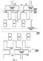
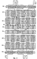
- FIG.2 is a plan view illustrating a "fast-access", alternate-metal, virtual-ground (AMG) electrically programmable read-only-memory (EPROM) 100 in accordance with the present invention
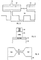
- FIG.3 is a plan view illustrating the increased width of the segment select transistors 116 in accordance with the present invention.
- FIG.4 is a plan view illustrating the formation of the field oxide regions in a P-type semiconductor substrate 100.
- FIG.5 and 6 are cross-sectional diagrams taken along lines 4A-4A.
- FIG.7 is a plan views illustrating the initial formation of the floating gates.
- FIGs. 8A-8C are cross-sectional diagrams taken along lines 7A-7A, 7B-7B, and 7C-7C, respectively.
- FIG. 9 is a plan view illustrating a plurality of strips 130 formed over the layer of ONO 124.
- FIGs. 10A-10D are cross-sectional diagrams taken along lines 7A-7A, 7B-7B, 7C-7C, and 7C-7C, respectively.
- FIG. 11 is a plan view illustrating the formation of the word lines WL1-WLn, the access select lines ASL1-ASLn, and the segment lines SSL1-SSLn.
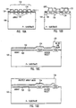
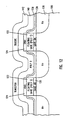
- FIG. 12 is a cross-sectional view taken along lines 11A-11A.
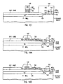
- FIGs. 13, 14A, and 14B are cross-sectional diagrams taken along lines 11B-11B.
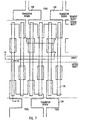
- FIGs. 15 and 16 are schematic diagrams that illustrate the operation of the fast-access EPROM of the present invention.
- FIG. 2 shows a plan view that illustrates a "fast-access", alternate-metal, virtual-ground (AMG) electrically programmable read-only-memory (EPROM) 100 in accordance with the present invention.
- AMG alternate-metal, virtual-ground
- EPROM electrically programmable read-only-memory
- the present invention increases the maximum current that can be driven by the segment select transistors by eliminating the even numbered segment select transistors in every other row of segment select transistors, and the odd numbered segment select transistors in the remaining rows, and by changing the current path through the segment so that the current flows from a segment select transistor in one row of segment select transistors to a segment select transistor in an adjacent row of transistors.
- the maximum width of the segment select transistors can be substantially increased, thereby providing the required programming current, while at the same time maintaining the required isolation between adjacent segment select transistors.
- EPROM 100 includes a semiconductor substrate 110 of P-type conductivity and a series of spaced-apart, parallel, bit lines BL1-BLn which are formed in substrate 100.
- a plurality of spaced-apart memory cells 112 are formed in a plurality of rows so that, in each row of memory cells 112, one memory cell 112 is formed between each pair of bit lines BL.
- a plurality of spaced-apart access select transistors 114 are formed in a plurality of pairs of rows so that, in each row of access select transistors 114, one access select transistor 114 is formed between every other pair of bit lines BL, and so that, in each pair of rows, one access select transistor 114 is formed between each pair of bit lines BL.
- EPROM 100 additionally includes a series of word lines WL1-WLn, which are formed so that each word line WL contacts each memory cell 112 in a row of memory cells 112, and a series of access select lines ASL1-ASLn, which are formed so that each access select line ASL contacts each of the access select transistors 114 in a row of access select transistors 114.
- EPROM 100 also includes a plurality of segment select transistors 116 which are formed in a plurality of rows so that, in each row of segment select transistors 116, one segment select transistor 116 contacts every fourth bit line BL.
- segment select transistors 116 in a row of segment select transistors 116 are staggered with respect to the segment select transistors 116 in each adjoining row so that every other bit line BL is contacted by one segment select transistor 116.
- a series of segment lines SSL1-SSLn are formed so that each segment line SSL contacts each of the segment select transistors 116 in a row of segment select transistors 116.
- FIG. 3 shows a plan view that illustrates the increased width of the segment select transistors 116 in accordance with the present invention.
- the maximum width of a segment select transistor in a conventional fast-access AMG EPROM which has been fabricated with a 0.8 micron process is limited to approximately 1.7 microns. This limitation results from the 3.4 micron pitch of two bit lines (every second bit line is contacted by one segment select transistor in each row of segment select transistors), less the 1.7 micron isolation width that is required between adjacent segment select transistors.
- the maximum width of a segment select transistor 116 is defined by the distance D 1 , which represents the 6.8 micron pitch of four bit lines, less the distance D 2 , which represents the 1.7 micron isolation width that is required between adjacent segment select transistors 116.
- the present invention substantially increases the maximum width of the segment select transistors 116 from approximately 1.7 microns (the 3.4 micron two bit line pitch less the 1.7 micron isolation width) to approximately 5.1 microns (the 6.8 micron four bit line pitch less the 1.7 micron isolation width). Accordingly, the present invention provides a delta increase of approximately 3.4 microns.
- each segment select transistor 116 can be formed so that the maximum current that can be driven by the segment select transistors 116 is equal to the current which is required by the memory cells during programming to insure that the memory cells of the array are properly programed.
- FIGs. 4-14 show plan and cross-sectional views that illustrate the steps for forming a "fast-access", AMG EPROM in accordance with the present invention.
- substrate 100 includes a plurality of access select regions, where the to-be-formed access select transistors will be formed, a plurality of segment select regions where the segment select transistors and the metal bit line contacts will be formed, and a plurality of array regions, where the to-be-formed memory cells will be formed.
- FIG. 4 shows a plan view that illustrates the formation of the field oxide regions in a P-type semiconductor substrate 100.
- FIGs. 5 and 6 show cross-sectional diagrams taken along lines 4A-4A.
- the field oxide regions are first formed by growing a layer of pad oxide 122 approximately 20nm (200 ⁇ ) thick over substrate 100. This is followed by the deposition of an overlying layer of nitride 124 approximately 200nm (2,000 ⁇ ) thick. Next, a field oxide mask 126 is formed over the nitride/pad oxide composite and patterned to define a plurality of rows of spaced-apart, contact-isolation field oxide regions FOXC, and a plurality of rows of spaced-apart transistor-isolation field oxide regions FOXT.
- the unmasked areas are etched until the underlying layer of nitride 124 is removed. As a result of this etching step, a plurality of pad oxide regions are exposed.
- the field oxide mask is stripped.
- a P-field implant mask is formed and patterned to protect portions of the periphery. The unmasked regions of pad oxide regions are then implanted with BF 2 at 50KeV to form implant regions which have an implant concentration of approximately 4 X 10 13 /cm 2 .
- the resulting device is oxidized to form the contact-isolation field oxide regions FOXC and the transistor-isolation field oxide regions FOXT.
- a transistor region 128 is formed between each adjacent pair of field oxide regions FOXC.
- the transistor regions 128 in one row of field oxide regions FOXC are staggered with respect to the transistor regions 128 in an adjacent row of field oxide regions FOXC.
- the contact-isolation field oxide regions FOXC are utilized to isolate the to-be-formed metal bit line contacts, the segment select transistors, and the access transistors in the first row of access transistors, while the transistor-isolation field oxide regions FOXT are utilized to isolate the to-be-formed access transistors in the second row of access transistors.
- the fabrication steps utilized to form the field oxide regions FOXC and FOXT are conventional and well known in the art.
- the next step is to set the channel threshold voltages for the to-be-formed memory cells.
- the threshold voltages are set by first removing the nitride/pad oxide composite layer. Next, a layer of sacrificial oxide (not shown) is grown on the exposed substrate 100. Following this, a threshold voltage mask is formed over the layer of sacrificial oxide and patterned to protect the periphery.
- the semiconductor substrate 100 underlying the unmasked areas of sacrificial oxide is implanted with B 11 at 40KeV to form an implant concentration of approximately 5 X 10 12 /cm 2 .
- the threshold voltage mask is stripped and the layer of sacrificial oxide is removed.
- the fabrication steps utilized to set the channel threshold voltages are also conventional and well known in the art.
- FIG. 7 shows a plan view that illustrates the initial formation of the floating gates.
- FIGs. 8A-8C show cross-sectional diagrams taken along lines 7A-7A, 7B-7B, and 7C-7C, respectively.
- the floating gates are first formed by growing a layer of gate oxide 120 approximately 15-20 nm (150-200 ⁇ ) thick over substrate 100.
- a layer of polysilicon (polyl) 122 approximately 150 nm (1,500 ⁇ ) thick is deposited over the layer of gate oxide 120 and the field oxide regions FOXC and FOXT.
- the layer of polyl 122 is then doped in a conventional manner.
- the floating gates of the array are formed from the layer of polyl 122.
- a composite dielectric layer of oxide/nitride/oxide (ONO) 124 is formed on the layer of polyl 122.
- a photoresist mask 126 is formed over the layer of ONO 124 and patterned to expose the segment select region and to define a plurality of spaced-apart parallel strips on the layer of ONO 124.
- FIG. 9 shows a plan view that illustrates a plurality of strips 130 formed over the layer of ONO 124.
- the ends of four adjacent strips are formed over one field oxide region FOXC in one row of field oxide regions FOXC.
- the opposite ends of a first two of the four adjacent strips are formed over a field oxide region FOXC in an adjacent row, while the opposite ends of a second two of the four adjacent strips are formed over an adjacent field oxide region FOXC in the adjacent row.
- the unmasked layer of ONO 124 and underlying layer of polyl 122 are then plasma etched to form a plurality of spaced-apart, parallel strips 132 of ONO/polyl.
- photoresist mask 126 is stripped.
- the ends of four strips 132 of ONO/poly are formed on one field oxide region FOXC, while the opposite ends are formed on two adjacent field oxide regions FOXC in an adjacent row.
- the layer of ONO 124 and the underlying layer of poly 122 are removed from the segment select region.
- FIGs. 10A-10D show cross-sectional diagrams taken along lines 7A-7A, 7B-7B, 7C-7C, and 7C-7C, respectively.
- a layer of thin edge oxide 134 is grown along the sides of the ONO/polyl strips 132 and over substrate 100.
- a bit line mask 133 is formed to protect the segment select regions and the periphery.
- arsenic is implanted into substrate 100 through the layer of oxide 134 to define the N+ bit lines 136.
- the bit line mask 133 is stripped.
- a layer of differential oxide 138 (see FIG. 12) is grown over the N+ bit lines 136.
- the layer of differential oxide 138 must be at least as thick as the layer of ONO 124 to avoid trenching of the substrate during a subsequent self aligned etch step which forms each of the cells and access transistors of the array.
- the segment select transistor are initially formed in the segment select regions while a plurality of MOS transistors can be initially formed in the periphery.
- the typical AMG EPROM includes a number of MOS transistors that function, for example, as current sense detectors, amplifiers, and address decoders.
- the segment select transistors and the peripheral MOS devices are first formed by forming a protect array mask 139 over the array and access select regions of substrate 100.
- the remaining layer of oxide is etched from the segment select regions and the periphery. Once the remaining layer of oxide has been removed, the protect array mask 139 is stripped.
- a second layer of gate oxide 150 (see FIGs. 13 and 14A) approximately 20nm (200 ⁇ ) thick is grown on the P-type semiconductor substrate in the segment select region and the periphery.
- the next step is to set the channel threshold voltages for each of the to be formed segment select and MOS transistors.
- the threshold voltages are set by forming and patterning a threshold mask, and then implanting a P-type dopant through the unmasked layer of gate oxide. Following this, the threshold voltage mask is stripped.
- FIG. 11 shows a plan view that illustrates the formation of the word lines WL1-WLn, the access select lines ASL1-ASLn, and the segment lines SSL1-SSLn.
- FIG. 12 shows a cross-sectional view taken along lines 11A-11A.
- FIGs. 13, 14A, and 14B show cross-sectional diagrams taken along lines 11B-11B.
- a layer of second polysilicon (poly2) 140 approximately 150nm (1,500 ⁇ ) is deposited over the surface of the entire device and doped in a conventional manner.
- this is followed by the deposition of an overlying layer of tungsten silicide 142 approximately 200nm (2,000 ⁇ ) thick.
- the control gates of the cells are formed by the portion of the composite layer of tungsten silicide/poly2 that is formed over the floating gates.
- a word line mask 145 is then formed over the tungsten silicide/poly2 composite and patterned to define the word lines WL1-WLn, the access select lines ASL1-ASLn, the segment lines SSL1-SSLn, and the gate electrodes of the peripheral MOS devices.
- the tungsten silicide/poly2 composite is etched until the unmasked layers of tungsten silicide, and poly2 have been removed.
- the access transistors are EPROM cells which have a larger width than the array flash EPROM cells. This allows the access transistors to drive larger currents than the array cells.
- the word line mask is UV-hardened and a self-aligned etch (SAE) mask 146 is formed so that the overlying tungsten silicide/poly2 composite can be used as a mask for a self-aligned etch of the ONO/poly1 composite.
- SAE mask 146 is formed to also protect the segment select regions. This then is followed by a stacked etch of the ONO/polyl composite to define each of the memory cells and access transistors.
- the SAE mask 146 is removed.
- a source/drain mask 152 is formed and patterned to define the N+ source and drain regions 148 of the segment select transistors, and the source and drain regions of the peripheral MOS devices.
- the P-type semiconductor substrate 100 underlying the unmasked areas is implanted with arsenic through the layer of gate oxide 150 to a depth of 0.2 to 0.3 microns. As shown in FIG. 14A, the implant is self-aligned to the edges of the layer of poly2 140.
- the source/drain mask 152 is then stripped. Next, as shown in FIG.
- the width of the remaining segment select transistors can be substantially increased.
- the maximum current that can be driven by the segment select transistors can be substantially increased.
- FIGs. 15 and 16 show schematic diagrams that illustrate the operation of the fast-access EPROM of the present invention.
- segment line 1, segment line 2, and word line 1 are set to a programming voltage (12 volts).
- access select lines 1 and 4 are set to a supply voltage (5-7 volts), while access select lines 2 and 3 and word line 2 are held at ground.
- bit line N-1 is held at ground, bit line N is taken to the supply voltage (5-7V), and bit line N+1 is allowed to float.
- a current path is established from segment select transistor SST1, through access select transistor AST1, through cell A, and to segment select transistor SST2.
- the bias conditions of cell A cause hot electron injection from the drain side to the floating gate of cell A.
- segment line 1, segment line 2, and word line 1 are set to the programming voltage.
- Access select lines 2 and 3 and word line 2 are set to the supply voltage (5-7 volts), while access select lines 1 and 4 and word line 2 are held at ground.
- bit line N-1 is set to the supply voltage, bit line N is held at ground, and bit line N-2 is allowed to float.
- segment lines 1 and 2 access select lines 1 and 4, and word line 1 are set to the supply voltage, while access select lines 2 and 3 and word line 2 are held at ground.
- bit lines N-1, N, and N+1 are precharged to a read voltage (1.5-2V). Once the bias conditions are set, bit line N is pulled down to ground, bringing the intermediate source to ground.
- bit lines N-1, N, and N-2 are precharged to a read voltage (1.5-2V). Once the bias conditions are set, bit line N-1 is pulled down to ground, bringing the intermediate source to ground.
- a flash EPROM may be formed wherein the substrate is formed in a semiconductor material of N-type conductivity so that the substrate functions as a P-well.
- the process for forming a well of P-type conductivity in an N-type semiconductor material is well known in the art.
- every other bit line BL of the series of bit lines BL1-BLn may be formed as a graded N + /N - bit line by masking alternate bit lines, followed by a phosphorous implant.
Landscapes
- Engineering & Computer Science (AREA)
- Microelectronics & Electronic Packaging (AREA)
- Non-Volatile Memory (AREA)
- Semiconductor Memories (AREA)
Claims (11)
- Segmentierter, elektrisch programmierbarer Nur-Lese-Speicher (100), der in einem Halbleitersubstrat (110) gebildet ist, wobei die Segmente aufweisen:dadurch gekennzeichnet, daßeine Anzahl von beabstandeten, parallelen Bitleitungen (BL), die in dem Halbleitersubstrat so ausgebildet sind, daß sich jede Bitleitung von einer ersten Seite des Segments zu einer zweiten Seite des Segments erstreckt,eine Anzahl von beabstandeten Speicherzellen (112), die in einer Anzahl von Reihen so ausgebildet sind, daß eine Speicherzelle in jeder Reihe von Speicherzellen auf dem Substrat zwischen jeweils zwei aneinandergrenzenden Bitleitungen ausgebildet ist,eine Anzahl von Wortleitungen (WL), die so ausgebildet sind, daß jede Wortleitung jede Speicherzelle in einer Reihe von Speicherzellen kontaktiert,eine Anzahl von beabstandeten Zugriffsauswahltransistoren (114), die in zwei Paaren von Reihen ausgebildet sind, wobei ein erstes Reihenpaar an der ersten Seite des Segmentes und ein zweites Reihenpaar an der zweiten Seite des Segmentes so ausgebildet sind, daß in jeder Reihe von Zugriffsauswahltransistoren ein Zugriffsauswahltransistor auf dem Substrat zwischen jeweils dem anderen Paar aneinandergrenzender Bitleitungen ausgebildet ist, und so, daß in jedem Paar von Reihen von Zugriffsauswahltransistoren nur ein Zugriffsauswahltransistor zwischen jeweils zwei aneinandergrenzenden Bitleitungen ausgebildet ist, undeine Anzahl von Zugriffsauswahlleitungen (ASL), die so ausgebildet sind, daß jede Zugriffsauswahlleitung jeden der Zugriffsauswahltransistoren in einer Reihe von Zugriffsauswahltransistoren kontaktiert,eine Anzahl von Segmentauswahltransistoren (116), die in einer Anzahl von Reihen von Segmentauswahltransistoren ausgebildet sind und mit den Bitleitungen auf der ersten und der zweiten Seite des Segmentes in versetzter Anordnung verbunden sind, undeine Anzahl von Segmentleitungen (SSL), die so ausgebildet sind, daß jede Segmentleitung jeden der Segmentauswahltransistoren (116) in einer Reihe von Segmentauswahltransistoren kontaktiert,
die Anzahl von Segmentauswahltransistoren (116) so ausgebildet sind, daß nur jede vierte Bitleitung der Bitleitungen an der ersten Seite des Segments mit einem Segmentauswahltransistor verbunden ist, und so, daß nur jede vierte Bitleitung der Bitleitungen an der zweiten Seite des Segments mit einem Segmentauswahltransistor verbunden ist, wobei die Segmentauswahltransistoren, die mit den Bitleitungen an der ersten Seite verbunden sind, versetzt mit Bezug auf die Segmentauswahltransistoren sind, die mit den Bitleitungen an der zweiten Seite verbunden sind, so daß jede abwechselnde Bitleitung durch einen Segmentauswahltransistor kontaktiert ist. - Speicher nach Anspruch 1 und mit ferner einer Anzahl von Segmentleitungen (SSL), die so ausgebildet sind, daß eine erste Segmentleitung jeden der Segmentauswahltransistoren kontaktiert, die mit den Bitleitungen an der ersten Seite verbunden sind, und eine zweite Segmentleitung jeden der Segmentauswahltransistoren kontaktiert, die mit den Bitleitungen an der anderen Seite verbunden sind.
- Segment nach Anspruch 1,
wobei jede zweite Bitleitung der Anzahl von Bitleitungen eine gradierte N+/N-Bitleitung aufweist. - Verfahren zum Programmieren einer ausgewählten Zelle in einem Segment eines elektrisch programmierbaren Nur-Lese-Speichers, der in einem Halbleitersubstrat ausgebildet ist, wobei das Verfahren die Schritte aufweist:Vorsehen eines elektrisch programmierbaren Nur-Lese-Speichers nach Anspruch 2, in dem ein Segmentauswahltransistor in der ersten Segmentleitung der ausgewählten Zelle entspricht und ein Segmentauswahltransistor in der zweiten Segmentleitung der ausgewählten Zelle entspricht,Einstellen der ersten und der zweiten Segmentleitung auf eine Programmierspannung,Einstellen einer Zugriffsauswahlleitung des ersten Paares von Zugriffsauswahlleitungen und einer Zugriffsauswahlleitung des zweiten Paares von Zugriffsauswahlleitungen auf eine Versorgungsspannung,Einstellen der verbleibenden Zugriffsauswahlleitung des ersten Paares von Zugriffsauswahlleitungen und einer verbleibenden Zugriffsauswahlleitung des zweiten Paares von Zugriffsauswahlleitungen auf Masse,Einstellen der einen Wortleitung auf die Programmierspannung,Einstellen der Bitleitung, die den einen Segmentauswahltransistor in der ersten Segmentleitung kontaktiert, auf eine erste Spannung undEinstellen der Bitleitung, die den einen Segmentauswahltransistor in der zweiten Segmentleitung kontaktiert, auf eine zweite Spannung.
- Verfahren des Herstellens eines segmentierten, elektrisch programmierbaren Nur-Lese-Speichers nach Anspruch 1 auf einem Halbleitersubstrat (100),
wobei der Speicher eine Anzahl von beabstandeten, parallelen Bitleitungen (BL) in dem Halbleitersubstrat so aufweist, daß sich jede Bitleitung von einer ersten Seite des Segmentes zu einer zweiten Seite des Segments erstreckt,
wobei das Verfahren die Ausbildung einer Anzahl von Segmentauswahltransistoren so umfaßt, daß nur jede vierte Bitleitung der Bitleitungen an der ersten Seite des Segmentes mit einem Segmentauswahltransistor verbunden ist, und so, daß nur jede vierte Bitleitung der Bitleitungen an der zweiten Seite des Segments mit einem Segmentauswahltransistor verbunden ist, wobei die Segmentauswahltransistoren, die mit den Bitleitungen an der ersten Seite verbunden sind, mit Bezug auf die Segmentauswahltransistoren, die mit den Bitleitungen an der zweiten Seite verbunden sind, gestaffelt angeordnet sind, derart, daß jede zweite Bitleitung mit einem Segmentauswahltransistor verbunden ist. - Verfahren nach Anspruch 5, mit ferner den Schritten:Ausbilden einer Anzahl von Feldoxidbereichen (FOXC) entlang einer ersten Seite und einer zweiten Seite des Segmentes zum Definieren einer Reihe von beabstandeten Transistorbereichen (128) entlang der ersten und der zweiten Seite derart, daß jeder angrenzende Transistorbereich durch einen Feldoxidbereich separiert und teilweise umgeben wird,Ausbilden einer Schicht aus erstem dielektrischen Material (320) über dem Halbleitersubstrat,Ausbilden einer Schicht von leitendem Material (122) über der Schicht des ersten dielektrischen Materials,Ausbilden einer Schicht aus zweitem dielektrischen Material (124) über der Schicht des leitenden Materials,Strukturieren und Entfernen von Teilen der Schicht des zweiten dielektrischen Materials und der unterliegenden Schicht des leitfähigen Materials zum Freilegen der 'Transistorbereiche (128) und Gebieten der Feldoxidbereiche zur Ausbildung einer Anzahl von beabstandeten parallelen Streifen (123) des zweiten dielektrischen Materials und des unterliegenden leitfähigen Materials, wobei erste Enden von vier aneinandergrenzenden Streifen über einem Feldoxidbereich (FOXC) an der ersten Seite des Segmentes gebildet werden und gegenüberliegende zweite Enden der vier Streifen mit zwei Enden auf jeweils einem Paar von aneinandergrenzenden Feldoxidbereichen an der zweiten Seite des Segments gebildet werden.
- Verfahren nach Anspruch 6,
wobei die Schicht des ersten dielektrischen Materials ein Gateoxid aufweist. - Verfahren nach Anspruch 6,
wobei die Schicht des leitfähigen Materials Polysilizium aufweist. - Verfahren nach Anspruch 6,
wobei die Schicht des zweiten dieelektrischen Materials eine Zusammensetzung aus Oxid-Nitrid-Oxid aufweist. - Verfahren nach Anspruch 6,
wobei das Substrat mit Leitfähigkeit vom P-Typ gebildet wird. - Verfahren nach Anspruch 10,
wobei das Substrat in einem Halbleitermaterial mit Leitfähigkeit vom N-Typ so gebildet wird, daß das Substrat als P-Bett funktioniert.
Applications Claiming Priority (3)
| Application Number | Priority Date | Filing Date | Title |
|---|---|---|---|
| US214818 | 1994-03-16 | ||
| US08/214,818 US5436478A (en) | 1994-03-16 | 1994-03-16 | Fast access AMG EPROM with segment select transistors which have an increased width |
| PCT/US1995/003058 WO1995025353A1 (en) | 1994-03-16 | 1995-03-13 | A fast access amg eprom with segment select transistors which have an increased width and method of manufacture |
Publications (2)
| Publication Number | Publication Date |
|---|---|
| EP0699345A1 EP0699345A1 (de) | 1996-03-06 |
| EP0699345B1 true EP0699345B1 (de) | 2002-10-02 |
Family
ID=22800533
Family Applications (1)
| Application Number | Title | Priority Date | Filing Date |
|---|---|---|---|
| EP95912876A Expired - Lifetime EP0699345B1 (de) | 1994-03-16 | 1995-03-13 | Amg eprom mit schneller zugriffszeit mit segment-auswahl-transistoren, welche eine vergrösserte weite haben und herstellungsverfahren |
Country Status (5)
| Country | Link |
|---|---|
| US (2) | US5436478A (de) |
| EP (1) | EP0699345B1 (de) |
| KR (1) | KR100365165B1 (de) |
| DE (1) | DE69528426T2 (de) |
| WO (1) | WO1995025353A1 (de) |
Families Citing this family (36)
| Publication number | Priority date | Publication date | Assignee | Title |
|---|---|---|---|---|
| KR940008722B1 (ko) * | 1991-12-04 | 1994-09-26 | 삼성전자 주식회사 | 반도체 메모리 장치의 워드라인 드라이버 배열방법 |
| US5808937A (en) * | 1994-12-16 | 1998-09-15 | National Semiconductor Corporation | Self-convergent method for programming FLASH and EEPROM memory cells that moves the threshold voltage from an erased threshold voltage range to one of a plurality of programmed threshold voltage ranges |
| US6768165B1 (en) | 1997-08-01 | 2004-07-27 | Saifun Semiconductors Ltd. | Two bit non-volatile electrically erasable and programmable semiconductor memory cell utilizing asymmetrical charge trapping |
| US6633496B2 (en) * | 1997-12-12 | 2003-10-14 | Saifun Semiconductors Ltd. | Symmetric architecture for memory cells having widely spread metal bit lines |
| US5847426A (en) * | 1997-12-15 | 1998-12-08 | National Semiconductor Corporation | Contactless flash EPROM using poly silicon isolation |
| ITTO980516A1 (it) * | 1998-06-12 | 1999-12-12 | St Microelectronics Srl | Procedimento per la fabbricazione di transistori di selezione di memor ie non volatili serial-flash, eprom, eeprom e flash-eeprom in configur |
| JP2000100974A (ja) * | 1998-07-21 | 2000-04-07 | Mitsubishi Electric Corp | 不揮発性半導体記憶装置およびその製造方法 |
| KR100699608B1 (ko) * | 1999-03-09 | 2007-03-23 | 코닌클리즈케 필립스 일렉트로닉스 엔.브이. | 비휘발성 메모리를 포함하는 반도체 디바이스 |
| US6584017B2 (en) | 2001-04-05 | 2003-06-24 | Saifun Semiconductors Ltd. | Method for programming a reference cell |
| KR100416599B1 (ko) * | 2001-05-31 | 2004-02-05 | 삼성전자주식회사 | 집적도와 독출동작 속도를 향상시키고 전력소모를감소시킬 수 있는 메탈 프로그래머블 롬의 메모리셀 구조 |
| US6700818B2 (en) | 2002-01-31 | 2004-03-02 | Saifun Semiconductors Ltd. | Method for operating a memory device |
| US6917544B2 (en) | 2002-07-10 | 2005-07-12 | Saifun Semiconductors Ltd. | Multiple use memory chip |
| US7136304B2 (en) | 2002-10-29 | 2006-11-14 | Saifun Semiconductor Ltd | Method, system and circuit for programming a non-volatile memory array |
| US7178004B2 (en) | 2003-01-31 | 2007-02-13 | Yan Polansky | Memory array programming circuit and a method for using the circuit |
| US7142464B2 (en) | 2003-04-29 | 2006-11-28 | Saifun Semiconductors Ltd. | Apparatus and methods for multi-level sensing in a memory array |
| US7123532B2 (en) | 2003-09-16 | 2006-10-17 | Saifun Semiconductors Ltd. | Operating array cells with matched reference cells |
| US7317633B2 (en) | 2004-07-06 | 2008-01-08 | Saifun Semiconductors Ltd | Protection of NROM devices from charge damage |
| US7095655B2 (en) | 2004-08-12 | 2006-08-22 | Saifun Semiconductors Ltd. | Dynamic matching of signal path and reference path for sensing |
| US7638850B2 (en) | 2004-10-14 | 2009-12-29 | Saifun Semiconductors Ltd. | Non-volatile memory structure and method of fabrication |
| US7535765B2 (en) | 2004-12-09 | 2009-05-19 | Saifun Semiconductors Ltd. | Non-volatile memory device and method for reading cells |
| CN1838323A (zh) | 2005-01-19 | 2006-09-27 | 赛芬半导体有限公司 | 可预防固定模式编程的方法 |
| US8053812B2 (en) | 2005-03-17 | 2011-11-08 | Spansion Israel Ltd | Contact in planar NROM technology |
| US7298651B2 (en) * | 2005-06-17 | 2007-11-20 | Intel Corporation | Architecture for virtual ground memory arrays |
| EP1746645A3 (de) | 2005-07-18 | 2009-01-21 | Saifun Semiconductors Ltd. | Speicherzellenanordnung mit sub-minimalem Wortleitungsabstand und Verfahren zu deren Herstellung |
| US7668017B2 (en) | 2005-08-17 | 2010-02-23 | Saifun Semiconductors Ltd. | Method of erasing non-volatile memory cells |
| US7221138B2 (en) | 2005-09-27 | 2007-05-22 | Saifun Semiconductors Ltd | Method and apparatus for measuring charge pump output current |
| US7352627B2 (en) | 2006-01-03 | 2008-04-01 | Saifon Semiconductors Ltd. | Method, system, and circuit for operating a non-volatile memory array |
| US7808818B2 (en) | 2006-01-12 | 2010-10-05 | Saifun Semiconductors Ltd. | Secondary injection for NROM |
| US7319611B2 (en) * | 2006-01-25 | 2008-01-15 | Macronix International Co., Ltd. | Bitline transistor architecture for flash memory |
| US7760554B2 (en) | 2006-02-21 | 2010-07-20 | Saifun Semiconductors Ltd. | NROM non-volatile memory and mode of operation |
| US7692961B2 (en) | 2006-02-21 | 2010-04-06 | Saifun Semiconductors Ltd. | Method, circuit and device for disturb-control of programming nonvolatile memory cells by hot-hole injection (HHI) and by channel hot-electron (CHE) injection |
| US8253452B2 (en) | 2006-02-21 | 2012-08-28 | Spansion Israel Ltd | Circuit and method for powering up an integrated circuit and an integrated circuit utilizing same |
| US7638835B2 (en) | 2006-02-28 | 2009-12-29 | Saifun Semiconductors Ltd. | Double density NROM with nitride strips (DDNS) |
| US7701779B2 (en) | 2006-04-27 | 2010-04-20 | Sajfun Semiconductors Ltd. | Method for programming a reference cell |
| US7605579B2 (en) | 2006-09-18 | 2009-10-20 | Saifun Semiconductors Ltd. | Measuring and controlling current consumption and output current of charge pumps |
| US7590001B2 (en) | 2007-12-18 | 2009-09-15 | Saifun Semiconductors Ltd. | Flash memory with optimized write sector spares |
Family Cites Families (6)
| Publication number | Priority date | Publication date | Assignee | Title |
|---|---|---|---|---|
| US5264718A (en) * | 1991-06-28 | 1993-11-23 | Texas Instruments Incorporated | EEPROM cell array with tight erase distribution |
| DE69207386T2 (de) * | 1992-06-01 | 1996-09-12 | Sgs Thomson Microelectronics | Verfahren zur Herstellung hochintegrierter kontaktloser EPROM's |
| EP0573169A1 (de) * | 1992-06-02 | 1993-12-08 | National Semiconductor Corporation | Segmentweise löschbares FLASH-EPROM |
| US5246874A (en) * | 1992-06-02 | 1993-09-21 | National Semiconductor Corporation | Method of making fast access AMG EPROM |
| US5315541A (en) * | 1992-07-24 | 1994-05-24 | Sundisk Corporation | Segmented column memory array |
| US5306658A (en) * | 1993-05-27 | 1994-04-26 | Texas Instruments Incorporated | Method of making virtual ground memory cell array |
-
1994
- 1994-03-16 US US08/214,818 patent/US5436478A/en not_active Expired - Lifetime
- 1994-08-03 US US08/285,650 patent/US5460990A/en not_active Expired - Lifetime
-
1995
- 1995-03-13 EP EP95912876A patent/EP0699345B1/de not_active Expired - Lifetime
- 1995-03-13 KR KR1019950705109A patent/KR100365165B1/ko not_active Expired - Lifetime
- 1995-03-13 DE DE69528426T patent/DE69528426T2/de not_active Expired - Lifetime
- 1995-03-13 WO PCT/US1995/003058 patent/WO1995025353A1/en not_active Ceased
Also Published As
| Publication number | Publication date |
|---|---|
| KR960702946A (ko) | 1996-05-23 |
| US5436478A (en) | 1995-07-25 |
| KR100365165B1 (ko) | 2003-05-09 |
| DE69528426T2 (de) | 2003-07-31 |
| WO1995025353A1 (en) | 1995-09-21 |
| DE69528426D1 (de) | 2002-11-07 |
| US5460990A (en) | 1995-10-24 |
| EP0699345A1 (de) | 1996-03-06 |
Similar Documents
| Publication | Publication Date | Title |
|---|---|---|
| EP0699345B1 (de) | Amg eprom mit schneller zugriffszeit mit segment-auswahl-transistoren, welche eine vergrösserte weite haben und herstellungsverfahren | |
| EP0694211B1 (de) | Verfahren zur reduzierung den abstandes zwischen den horizontalen benachbarten schwebenden gates einer flash eprom anordnung | |
| US5049515A (en) | Method of making a three-dimensional memory cell with integral select transistor | |
| US5907171A (en) | Method of making floating-gate memory-cell array with digital logic transistors | |
| US6058045A (en) | Serial flash memory | |
| CN1316625C (zh) | 非易失性存储器及其制造方法 | |
| JP3606596B2 (ja) | 集積デバイスの製造方法 | |
| US5379254A (en) | Asymmetrical alternate metal virtual ground EPROM array | |
| US5409854A (en) | Method for forming a virtual-ground flash EPROM array with floating gates that are self aligned to the field oxide regions of the array | |
| JPH06188396A (ja) | 電気的に消去できる無接点epromメモリデバイスの製造方法 | |
| JP3694329B2 (ja) | 高速アクセスamg・epromの製造方法 | |
| KR100284107B1 (ko) | 제3 폴리실리콘층을 이용하여 듀얼 폴리 비휘발성 메모리 소자를 제조하는 방법 | |
| JPH0745728A (ja) | 不揮発性eprom,eeprom又はフラッシュeepromメモリ、不揮発性メモリを形成するための中間構造、及びトンネル酸化物を保護する不揮発性eprom,eeprom又はフラッシュeepromメモリの製造方法 | |
| US20020135013A1 (en) | Segmented bit line EEPROM page architecture | |
| EP0698295B1 (de) | Verfahren zur Herstellung eines elektrisch programmierbaren Festwertspeichers | |
| EP0698286B1 (de) | Flash eprom-matrix mit virtueller erdung mit reduziertem zellenschrittabstand in der x-richtung | |
| JP2003051557A (ja) | 不揮発性半導体記憶装置 | |
| KR100289814B1 (ko) | 비휘발성메모리장치및그제조방법 | |
| US5151760A (en) | Integrated circuit with improved capacitive coupling | |
| KR100309139B1 (ko) | 비휘발성 메모리 소자 제조방법 | |
| US7300745B2 (en) | Use of pedestals to fabricate contact openings | |
| US6834011B2 (en) | Structure, fabrication method and operating method for flash memory | |
| KR19990006967A (ko) | 불휘발성 반도체 기억 장치 및 그 제조 방법 | |
| KR0161808B1 (ko) | 낸드형 불휘발성 반도체 메모리장치 및 그 제조방법 | |
| WO1995025352A1 (en) | A virtual-ground flash eprom with reduced-step-height field oxide regions in the array |
Legal Events
| Date | Code | Title | Description |
|---|---|---|---|
| PUAI | Public reference made under article 153(3) epc to a published international application that has entered the european phase |
Free format text: ORIGINAL CODE: 0009012 |
|
| 17P | Request for examination filed |
Effective date: 19951205 |
|
| AK | Designated contracting states |
Kind code of ref document: A1 Designated state(s): DE FR GB |
|
| RIN1 | Information on inventor provided before grant (corrected) |
Inventor name: BERGEMONT, ALBERT |
|
| 17Q | First examination report despatched |
Effective date: 19991206 |
|
| GRAG | Despatch of communication of intention to grant |
Free format text: ORIGINAL CODE: EPIDOS AGRA |
|
| GRAG | Despatch of communication of intention to grant |
Free format text: ORIGINAL CODE: EPIDOS AGRA |
|
| GRAH | Despatch of communication of intention to grant a patent |
Free format text: ORIGINAL CODE: EPIDOS IGRA |
|
| GRAH | Despatch of communication of intention to grant a patent |
Free format text: ORIGINAL CODE: EPIDOS IGRA |
|
| GRAA | (expected) grant |
Free format text: ORIGINAL CODE: 0009210 |
|
| AK | Designated contracting states |
Kind code of ref document: B1 Designated state(s): DE FR GB |
|
| PG25 | Lapsed in a contracting state [announced via postgrant information from national office to epo] |
Ref country code: FR Free format text: LAPSE BECAUSE OF FAILURE TO SUBMIT A TRANSLATION OF THE DESCRIPTION OR TO PAY THE FEE WITHIN THE PRESCRIBED TIME-LIMIT Effective date: 20021002 |
|
| REG | Reference to a national code |
Ref country code: GB Ref legal event code: FG4D |
|
| REF | Corresponds to: |
Ref document number: 69528426 Country of ref document: DE Date of ref document: 20021107 |
|
| PG25 | Lapsed in a contracting state [announced via postgrant information from national office to epo] |
Ref country code: GB Free format text: LAPSE BECAUSE OF NON-PAYMENT OF DUE FEES Effective date: 20030313 |
|
| EN | Fr: translation not filed | ||
| PLBE | No opposition filed within time limit |
Free format text: ORIGINAL CODE: 0009261 |
|
| STAA | Information on the status of an ep patent application or granted ep patent |
Free format text: STATUS: NO OPPOSITION FILED WITHIN TIME LIMIT |
|
| 26N | No opposition filed |
Effective date: 20030703 |
|
| GBPC | Gb: european patent ceased through non-payment of renewal fee |
Effective date: 20030313 |
|
| PGFP | Annual fee paid to national office [announced via postgrant information from national office to epo] |
Ref country code: DE Payment date: 20120328 Year of fee payment: 18 |
|
| REG | Reference to a national code |
Ref country code: DE Ref legal event code: R082 Ref document number: 69528426 Country of ref document: DE |
|
| REG | Reference to a national code |
Ref country code: DE Ref legal event code: R119 Ref document number: 69528426 Country of ref document: DE Effective date: 20131001 |
|
| PG25 | Lapsed in a contracting state [announced via postgrant information from national office to epo] |
Ref country code: DE Free format text: LAPSE BECAUSE OF NON-PAYMENT OF DUE FEES Effective date: 20131001 |