EP0698890A1 - Prüfung einer integrierten Schaltungsanordnung - Google Patents
Prüfung einer integrierten Schaltungsanordnung Download PDFInfo
- Publication number
- EP0698890A1 EP0698890A1 EP95305705A EP95305705A EP0698890A1 EP 0698890 A1 EP0698890 A1 EP 0698890A1 EP 95305705 A EP95305705 A EP 95305705A EP 95305705 A EP95305705 A EP 95305705A EP 0698890 A1 EP0698890 A1 EP 0698890A1
- Authority
- EP
- European Patent Office
- Prior art keywords
- programming
- integrated circuit
- circuit device
- storage elements
- voltage
- Prior art date
- Legal status (The legal status is an assumption and is not a legal conclusion. Google has not performed a legal analysis and makes no representation as to the accuracy of the status listed.)
- Granted
Links
- 238000012360 testing method Methods 0.000 title claims abstract description 99
- 230000015654 memory Effects 0.000 claims description 83
- 238000000034 method Methods 0.000 claims description 9
- 230000004044 response Effects 0.000 claims description 4
- 238000010998 test method Methods 0.000 claims description 3
- 238000010586 diagram Methods 0.000 description 8
- PWPJGUXAGUPAHP-UHFFFAOYSA-N lufenuron Chemical compound C1=C(Cl)C(OC(F)(F)C(C(F)(F)F)F)=CC(Cl)=C1NC(=O)NC(=O)C1=C(F)C=CC=C1F PWPJGUXAGUPAHP-UHFFFAOYSA-N 0.000 description 5
- 238000009966 trimming Methods 0.000 description 5
- 230000008901 benefit Effects 0.000 description 4
- 102000051619 SUMO-1 Human genes 0.000 description 2
- 108091007492 Ubiquitin-like domain 1 Proteins 0.000 description 2
- 238000002955 isolation Methods 0.000 description 2
- 238000010276 construction Methods 0.000 description 1
- 230000000694 effects Effects 0.000 description 1
- 238000011156 evaluation Methods 0.000 description 1
- 238000004519 manufacturing process Methods 0.000 description 1
- 230000008569 process Effects 0.000 description 1
- 230000009467 reduction Effects 0.000 description 1
- 239000004065 semiconductor Substances 0.000 description 1
- 230000003068 static effect Effects 0.000 description 1
- 239000000758 substrate Substances 0.000 description 1
- 230000007704 transition Effects 0.000 description 1
Images


Classifications
-
- G—PHYSICS
- G11—INFORMATION STORAGE
- G11C—STATIC STORES
- G11C29/00—Checking stores for correct operation ; Subsequent repair; Testing stores during standby or offline operation
- G11C29/04—Detection or location of defective memory elements, e.g. cell constructio details, timing of test signals
- G11C29/08—Functional testing, e.g. testing during refresh, power-on self testing [POST] or distributed testing
- G11C29/12—Built-in arrangements for testing, e.g. built-in self testing [BIST] or interconnection details
- G11C29/18—Address generation devices; Devices for accessing memories, e.g. details of addressing circuits
- G11C29/24—Accessing extra cells, e.g. dummy cells or redundant cells
-
- G—PHYSICS
- G11—INFORMATION STORAGE
- G11C—STATIC STORES
- G11C29/00—Checking stores for correct operation ; Subsequent repair; Testing stores during standby or offline operation
- G11C29/04—Detection or location of defective memory elements, e.g. cell constructio details, timing of test signals
-
- G—PHYSICS
- G11—INFORMATION STORAGE
- G11C—STATIC STORES
- G11C29/00—Checking stores for correct operation ; Subsequent repair; Testing stores during standby or offline operation
- G11C29/52—Protection of memory contents; Detection of errors in memory contents
Definitions
- This invention relates to testing an integrated circuit device, and in particular to testing an IC device which includes elements which can be programmed once but which cannot be reprogrammed or which are slow or awkward to reprogram.
- the invention concerns a method for testing such a device and a novel IC structure for implementing the test.
- the invention is particularly but not exclusively concerned with integrated circuit semiconductor memory devices.
- the present invention can be applied to any appropriate device, and is not restricted to any specific structure of device.
- the invention has particular advantage in a flash EPROM which includes electrically reprogrammable single transistor cells with a floating gate, and a plurality of non-reprogrammable elements or UPROM elements.
- the invention can also be applied where the UPROM elements can be reprogrammed but only by a slow or awkward process.
- UPROM cells are used on flash EPROMs (erasable programmable read only memories) to store redundancy information. Bits can also be used to alter a chip's functionality, either to enable optional functionality or to trim analogue voltages or timings. This "trimming" can help to make the chip more tolerant of manufacturing variations.
- the UPROM cells are programmed using a test mode by appropriately setting voltages using a program circuit. However, once a bit has been programmed into a UPROM cell, it is not possible to erase it, except possibly by erasing flash transistors used in the UPROM cell, but this is undesirable during testing as this programming and erasing would take a significant amount of time. Thus, it is not possible with existing memory devices to "try out” a trim setting before programming it to its final value.
- an integrated circuit device comprising: functional circuitry controllable in response to control signals; a plurality of storage elements which are not reprogrammable or which are slow to reprogram; a set of latches, each latch in the set being associated respectively with each storage element of a set of the plurality of storage elements for holding respective test data bits; and a set of switch circuits, each switch circuit connected to a respective one of said set of storage elements and to its associated latch and selectively operable to supply as an output a signal from one of the storage element and the latch to which it is connected, whereby, in use in a test mode, the latches hold test data bits for testing the device, the switch circuit being operated to supply said control signals from said test data bits and, in use in a normal mode, the switch circuits are operated to supply said control signals from said storage elements; wherein said functional circuitry includes programming circuitry for programming the storage elements.
- the invention is particularly applicable to an integrated circuit device wherein said functional circuitry includes an array of reprogrammable memory cells, the storage elements being non-reprogrammable or slow to reprogram relative to the reprogrammable memory cells.
- the programming circuitry can also be used for programming the reprogrammable memory cells.
- it can include a plurality of programmable load circuits for supplying programming signals; and a program controller circuit responsive to said control signals for determining the programming signals to be supplied by the programmable load circuits.
- a first set of programmable load circuits supplies programming signals to the storage elements and to the reprogrammable memory cells and a second set supplies programming signals only to the reprogrammable memory cells.
- the programmable load circuits can be arranged differently.
- a first set of programmable load circuits is dedicated to supply programming signals to the storage elements and a second set of programmable load circuits is dedicated to supply programming signals to the reprogrammable memory cells.
- all of the programmable load circuits are shared, that is they supply programming signals both to the storage elements and to the reprogrammable memory cells.
- a first set of the programmable load circuits is shared, and a second set is arranged to supply programming signals only to the storage elements.
- a set of the programmable load circuits is shared, one set is dedicated to the reprogrammable memory cells and another set is dedicated to the storage elements.
- the functional circuitry can include clock circuitry for supplying a clock signal for operation of the program control circuit, the frequency of the clock signal being controlled by the control signals.
- the functional circuitry can also include voltage supply circuitry for supplying an appropriate analogue voltage for operation of the integrated circuit device, the analogue voltage being determined by the control signals.
- the voltage supply circuitry can comprise a source voltage switch for selectively supplying an appropriate voltage to the sources of transistors within the memory array. Alternatively or additionally, it can comprise a programming voltage reference circuit for selectively supplying a reference voltage for programming.
- the invention provides a memory comprising: a first plurality of reprogrammable memory cells; a second plurality of electrically reprogrammable memory cells which are slow to reprogram relative to the reprogrammable memory cells; a set of latches, each latch in the set being associated respectively with each of a set of the second plurality of memory cells; a set of switch circuits, each switch circuit connected to a respective one of said set of memory cells and to its associated latch and selectively operable to supply as an output a signal from one of the memory cell and the latch to which it is connected whereby, in use in a test mode, the latches hold test data bits for testing the memory, the switch circuit being operated to output said test data bits and, in use in a normal mode, the switch circuits are operated to output data bits from said set of memory cells.
- UPROM cells the memory cells which are not reprogrammable or which are slow to reprogram are referred to herein as UPROM cells.
- the provision of a latch associated with each UPROM cell allows test data bits to be used for testing and for setting a final "trim". Once a satisfactory test has been carried out, the UPROM cells can be programmed in accordance with the test data bits for that test which were held in the latches. This dramatically enhances the options available for testing a memory device.
- each of the first plurality of reprogrammable memory cells is a single transistor with a floating gate which is electrically erasable and reprogrammable.
- the invention provides in a further aspect a method of testing an integrated circuit device comprising functional circuitry controllable in response to control signals and a plurality of storage elements which are not reprogrammable or which are slow to reprogram, the method comprising: loading test data bits respectively into each of a set of latches, each latch being associated with a respective one of a set of the plurality of storage elements; selecting a test mode in which the outputs of the latches provide the control signals for testing the memory; on completion of a satisfactory test, programming the storage elements in accordance with the test data bits which were held in the latches during the satisfactory test; and selecting a normal mode of operation in which the storage elements provide the control signals, wherein the functional circuitry includes programming circuitry for programming the storage elements.
- the invention also provides a method of testing a memory comprising a first plurality of reprogrammable memory cells and a second plurality of electrically reprogrammable memory cells which are slow to reprogram relative to the reprogrammable memory cells, the method comprising: loading test data bits respectively into each of a set of latches, each latch being associated with a respective one of a set of the second plurality of memory cells; selecting a test mode in which the outputs of the latches provide the test signal outputs for testing the memory; on completion of a satisfactory test, programming a second plurality of memory cells with the test data bits which were held in the latches during the satisfactory test; and selecting a normal mode of operation in which the outputs of the second plurality of memory cells provide control signals for the memory.
- the present invention can be applied to any appropriate integrated circuit device with non-reprogrammable or hard to reprogram storage elements.
- the invention has particular advantage in a flash memory having reprogrammable single transistor cells with a floating gate and separate UPROM cells.
- the basic principle of operation of one type of flash memory will be described hereinbelow with reference to a specific illustrative example.
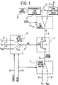
- Figure 1 illustrates a flash memory cell 2 comprising a single floating gate transistor 4 having a control gate CG, a source S, and a drain D.
- the source S of the floating gate transistor 4 is connected to an ARRAY GROUND signal on line 10.
- this line 10 can be at a ground voltage VGND or a high voltage Vpp.
- Voltage Vpp represents a programming potential (typically 12V) and voltage VGND represents device ground.
- Vpp is normally connected to array ground via a resistor (not shown).
- the source voltage switch 14 is connected to the voltage Vpp via line 34 and the voltage VGND via line 36.
- the control gate CG of the floating gate transistor 4 is connected to a gate voltage switch 12 by a word line (WL) 8 through a row decoder circuit not shown in Figure 1.
- the gate voltage switch 12 is further connected to voltages Vcc', Vpp and VGND on lines 26, 24 and 22 respectively.
- VCC' is at 5V for a 5V part or is boosted to about 5V (or above 4V) for a 3V part.
- These switches 14 and 12 each receive a control signal ERASE on line 28 and additionally the gate voltage switch 12 receives a control signal PROGRAM on line 30.
- the drain D of the floating gate transistor 4 is connected to a bit line switch 31 by a bit line (BL) 6.
- the bit line switch is further connected to the input of a programmable load circuit 32 on line 27 and the input of a sense amplifier circuit 29 on line 25.
- the output of the sense amplifier circuit 29 on line 23 forms a data line (DL).
- the switch 31 receives a control signal SELECT on line 21.
- the programmable load circuit 32 receives load control signals on lines 38.
- the flash memory has three modes of operation: program, erase and read. Each of these modes will be described hereinafter with reference to Figure 1.
- the program mode involves writing a "0" to a memory cell or group of memory cells
- the erase mode involves storing "1"s
- the read mode involves reading a cell to establish whether it is programmed or erased, i.e. contains either a "0" or a "1".
- the control signal PROGRAM on line 30 is set such that the gate voltage switch 12 is configured to connect the voltage Vpp on line 24 to the control gate CG of transistor 4 via word line 8.
- the source voltage switch 14 is configured to connect the voltage VGND on line 36 to the source of transistor 4 via the ARRAY GROUND signal line 10.
- the control signal SELECT on line 21 is set such that the bit line on line 6 is connected to the programmable load 32 by line 27.
- the load control signals 38 are set such that the programmable load 32 is controlled such that a voltage of about 5V is on the drain D of the transistor 4 via the bit line 6. As a result of these signals applied to the transistor 4, the floating gate becomes negatively charged.
- the negative charge shifts the threshold voltage of the floating gate transistor making it less conductive.
- the amount of negative charge accumulated at the floating gate depends on the duration for which the control signal PROGRAM is set. In this way, a "0" is written into the cell. Normally, several program pulses may be needed, each pulse being followed by a verify cycle.
- the control signal ERASE on line 28 is set such that the gate voltage switch 12 is configured to connect the voltage VGND on line 22 to the control gate CG of the transistor 4 via the word line 8, and such that the switch 14 is configured to connect the voltage Vpp on line 34 to the source S of the transistor 4 via the ARRAY GROUND line 10.
- the control signal SELECT on line 21 is again set such that the bit line 6 is disconnected so that it floats.
- the floating gate transistor is fabricated such that the source region in the substrate underlies the floating gate, any negative charge on the floating gate will be reduced. The amount of negative charge removed from the floating gate depends on the duration for which the ERASE signal on line 28 is set. The reduction of negative charge shifts the threshold voltage of the floating gate transistor making it more conductive. In this way the state of the cell is restored to "1". Normally, several erase pulses are required, each erase pulse being followed by a verify cycle.
- the Vcc' signal on line 26 is connected by the source voltage switch 12 to the control gate of the transistor 4 via the word line 8 and the voltage VGND on line 36 is connected to the source of the transistor 4 via the ARRAY GROUND signal line 10.
- the bit line 6 is biased to approximately 1 volt prior to a read operation by a bit line load (not shown) within the sense amplifying circuit.
- a bit line load not shown
- the conductivity of the cell is such that current passes through the cell when the bit line is connected for sensing.
- For a programmed cell substantially no current passes through the cell.
- the current passed by the cell is compared with a reference current to detect the status of the cell.
- Figure 2 illustrates a flash memory array 50 comprising a plurality of flash memory cells FMoo ... FMnm, arranged in rows and columns, each of which can be the same as the cell 2 shown in Figure 1.
- the gates of the transistors in each memory cell in a row are commonly connected to a respective word line WLo ... WLn addressable by a row line decode circuit 56 which receives the row address 64.
- the gate voltage switch 12 responds to the control signals PROGRAM and ERASE on line 30 and 28 respectively, and supplies the appropriate gate voltage Vccx on line 29 to be switched to the addressed wordline through the row decode circuit 56.
- the drains of each transistor in a column are commonly connected by bit lines BLo ... BLm to a column line decode circuit 58.
- the column line decode circuit can be considered as a plurality m of the bit line switch circuits 31, with the SELECT signal being generated responsive to the column address 38.
- the output of the column line decode circuit 58 on line 25 is a read output and is connected to the sense amplifier circuit 29.
- the column line decode circuit receives a write input on line 27 from the programmable load circuit 32.
- the programmable load circuit is controlled by the load control signals 38.
- the bit lines BLo to BLm are selectively connected to the programmable load circuit 32.
- the selected bit line (or bit lines) is connected to the sense amplifier circuit 29.
- the sense amplifier circuit 29 also receives a reference signal REF on line 72 and generates an output signal on the data line (DL) on line 23.
- the flash memory array 50 also includes a plurality of UPROM cells UC0 ... UCn, as shown in Figure 3.
- a single row of UPROM cells is shown in Figure 3 but it will be appreciated that any number of UPROM cells could be provided in accordance with requirements. Where there is more than one row, a row decode for the UPROM cells will be required.
- These UPROM cells differ from the flash memory cells FC00 ... FCnm in that they comprise a more complex arrangement of transistors than the single floating gate transistor which constitutes a flash memory cell and in that, once they have been programmed, they cannot be reprogrammed either at all or easily.
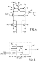
- a UPROM element is shown in Figure 4.
- the UPROM element 94 shown in Figure 4 comprises first and second floating gate transistors 78,80. These transistors can be as shown in Figure 1 and operate in a similar manner.
- the sources of the transistors 78,80 are both connected to ground (VGND). There is no need to connect them to a source voltage switch for selectively connecting them to Vpp as in Figure 1, because these transistors are not intended to be erased and reprogrammed after initial programming, although this could be done if desired.
- the gates of the transistors are connected to a UPROM wordline UWL, which is connected to a voltage switch 100 for selectively connecting the wordline UWL to Vpp, Vcc or VGND.
- the voltage input marked Vpp in Figure 3 could be connected to the voltage Vccx in Figure 2 if desired.
- the drains of the transistors are connected to the bit lines UBL, UBL ⁇ for the cell.
- the UPROM bit lines UBL0, UBL0 ⁇ , UBL1, UBL1 ⁇ ... UBLn, UBLn ⁇ are connected to a UPROM column decode circuit 102 through which a programming voltage is selectively connected to the bit lines from a programmable load 104.
- the programmable load 104 receives load enable and program load signals on lines 106,108 and the higher supply voltage Vpp on line 110.
- This programming load circuit 104 acts to apply to the drains of the transistors 78,80 voltages to program one of the flash transistors using programming voltage levels discussed earlier.
- the drains of the flash transistors 78,80 are connected through switch transistors 84,86 to a pair of p-channel cross-coupled transistors 88,90 which cooperate to remove DC current in a known manner when the cell is programmed. These cross-coupled transistors in turn are connected to the power supply voltage Vcc.
- the output 93 of the UPROM element 94 is taken between the transistor 90 and the switchable transistor 86 via an inverter 92. In a known memory, this output 93 is then supplied to other parts of the memory in a known fashion.
- the UPROM element 94 also includes an isolation transistor 82 which receives a disable signal on line 112. During programming, the disable signal is active so that the switch transistors 84,86 are off and the isolation transistor is on, in order to isolate the pair of p-channel cross-coupled transistors 88,90 from the high voltages used during programming.
- the switch transistors 84,86 receive a control signal RCASC from a UPROM reference generator circuit 114.
- a UPROM cell is selected for programming using the column decode circuit 102 which receives an address 118.
- This address can be provided by a subset of the address bits which are used to address the main memory array shown in Figure 2.
- the programmable load 104 contains a plurality of program loads, each program load being connected to a respective bit line of selected UPROM cells. In the described implementation, these are the same program loads that are used for programming the normal array 50, although different ones could be used if desired.
- each UPROM cell UC0...UC n shown in Figure 2 has the construction shown in block diagram in Figure 5. That is, it comprises a conventional UPROM element of the type shown in Figure 4 for example which is denoted by reference numeral 94 in Figure 5 and entitled UPROM. There is provided in parallel with this UPROM element a latch 96. The output of the UPROM element on line 93 and the output of the latch 96 are supplied to a multiplexor 98 which selectively switches one of the output of the UPROM element 94 and the latch 96 to provide output signals OUT0...OUT n ( Figure 3).
- the outputs OUT0...OUT n of the UPROM cells are used as signals for controlling other parts of the memory.
- control signals affect the following:
- Figure 6 is a block diagram of circuitry associated with a memory circuit exemplifying particular applications of the outputs OUT0 ...OUT n of the UPROM cells.
- seven sets of outputs are illustrated, 200,201,202,203,204, 205,206.
- the output signals OUT0...OUT n correspond to the outputs illustrated in Figure 3 and Figure 5.
- each output comes from the respective multiplexor 98 of the appropriate UPROM cell UC0...UC n .
- the outputs represent test data bits stored in the latch 96.
- the outputs represent data bits stored in the UPROM element 94.
- Reference numeral 260 denotes a memory circuit of the general type illustrated in Figure 2.
- the memory circuit includes a column decode circuit 58, a row decode circuit 56, a source voltage switch 52 and a sense amplifier 29.
- the sense amplifier is a dynamic sense amplifier and is controlled by a sense clock signal supplied from a sense amplifier clock circuit 207.
- the programmable load 32 for supplying programming signals to the memory array 50 via the column decode circuit 58 comprises a plurality of programmable load circuits 320...327 and 328,329.
- the first set of programmable load circuits 320...327 supplies programmable load signals to the normal memory array 50 of the memory circuit 260 and also to the column decode circuit 102 for the UPROM cells UC0...UC n .
- the second set of programmable load circuits 328,329 supply programming signals only to the memory array 50 of the memory circuit 260.
- the programming signals supplied by the programmable load circuits 320...329 are controlled by a program/erase controller 219 which takes the form of a state machine.
- the program/erase controller 219 also controls a program voltage reference circuit 220 which supplies a voltage reference for the column decode circuits 58,102.
- the program/erase controller 219 also controls the source voltage switch 52.
- Reference numeral 264 denotes feedback signals from other on-chip circuits, e.g. low Vcc detect.
- Reference numeral 262 denotes external signals from external circuits for implementing operations of the controller 219.
- a clock signal controls the timing of the program/erase controller.
- the clock signal is supplied by a clock circuit 214 while the controller 219 is activated, responsive to the signal Run on line 263.
- the integrated circuit also includes a supply voltage range control circuit 230 which can be programmed to implement a 5V mode, a 3.3V mode or to determine whether the supply voltage is 5V or 3.3V. It further generates a low power supply voltage signal, LOWVcc, when the power supply dips below a low level.
- the program/erase controller circuit 219 supplies program control signals 218 for controlling the programming signals for programming the FLASH array 50 and also the UPROM cells after a satisfactory test has been completed.
- the program voltage reference circuit 220 and the programmable load circuits 320...327 are controlled by the program/erase controller circuit 219.
- operation of the program/erase controller circuit is affected by the second and third sets of outputs, 201,202 from the UPROM cells. Further, the voltage supplied by the program voltage reference circuit 220 is affected by the fifth set of outputs 204.
- the first set of outputs 200 from the UPROM cells control timing of the sense amplifier clock circuit 207 by providing a delay trim signal.
- the timing of the sense amplifier 29 can be first tested using test data bits stored in the latches 96 and then programmed into the UPROM elements when the timing is satisfactory.
- Reference numeral 261 denotes control signals used for controlling the sense amplifier clock circuit for starting a read operation.
- the second set of outputs 201 from the UPROM cells provide a frequency trim signal to the clock circuit 214 for adjusting the frequency of the clock signal supplied to the program/erase controller 219.
- the third set of outputs 202 control functional options for the program/erase controller 219, for example to determine whether or not the state machine will accept CPU or embedded program/erase commands, as discussed above.
- the fourth set of outputs 203 controls the source voltage switch 52 to trim the resistance through which the analogue voltage is supplied by the source voltage switch.
- the fifth set of outputs 204 controls the program voltage reference circuit 220 to trim the analogue voltage supplied as a program voltage reference to the column decode circuits 58,102.
- the seventh set of outputs 206 control the Vcc range control circuit 230 to program the circuit to operate at a nominal supply voltage Vcc of 5V, 3.3V or in an autodetect mode which will work for both.
- the sixth set of outputs 205 are used for optional functionality of the memory circuit 206.
- the present invention has a particular advantage where some of the outputs from the UPROM cells (in this case sets 201,202,204) are used to modify programming signals used for programming the UPROM cells. That is, respective sets of test data bits can be loaded into the latches 96 and used to generate the output sets 201,202,204 for the clock circuit 214, program/erase controller circuit 219 and program voltage reference circuit 220. This allows optimisation of the programming settings for programming the UPROM elements, without having had to program the UPROM elements already. Without a latch associated with each UPROM element in the manner of the present invention, it would not be possible to achieve this.
- the latch 96 receives data bits on the line marked DATA and is controlled by a LOAD LATCH signal.
- the multiplexor 98 is controlled by a USE LATCH signal.
- the multiplexor 98 is set so that the output signal OUT comes from the UPROM element 94.
- the signal USE LATCH which controls the multiplexor can be activated so that the output signal OUT comes from the latch 96 instead of from the UPROM element 94.
- the memory can be tested in accordance with a test data bit in the latch 96. If the test of the memory is not satisfactory, the test data bit in the latch 96 is changed and a second test is run. When the results of the test are satisfactory in this test mode, the UPROM elements 94 can be programmed in accordance with the test data bit which was stored in the latch 96 when the successful test result was gained. Programming of the UPROM element 94 is done in a known manner as already discussed.
- a "satisfactory test” is either one which determines the accuracy of the test data bits which have actually been used in the test, or one which allows the results of the test to be used to determine required option bits.
- Loading of the test data bit into the latch 96 is done in another test mode in which the signal LOAD LATCH is activated. In this mode, the test data bit is loaded into the latch 96 on the data line DATA.
- test mode to load the desired test data bits into the latches is selected by setting the LOAD LATCH signal.
- test data bits are loaded into the latches along the data lines DATA.
- the test mode is then selected which causes the bits held in the latches 96 to be output by the multiplexor 98 by setting the USE LATCH signal.
- Normal memory operations can then be carried out while this test mode remains active, that is using the test data bits stored in the latches 96.
- the UPROM elements can finally be programmed with these test data bits.
- the LOAD LATCH test mode is then released so that the outputs OUT are taken from the UPROM elements for normal use.
- the LOAD LATCH test mode and the USE LATCH test mode can be selected in any known fashion, for example by holding an input pin at a superhigh voltage.
Landscapes
- Read Only Memory (AREA)
- For Increasing The Reliability Of Semiconductor Memories (AREA)
- Tests Of Electronic Circuits (AREA)
Applications Claiming Priority (2)
| Application Number | Priority Date | Filing Date | Title |
|---|---|---|---|
| GB9417268 | 1994-08-26 | ||
| GB9417268A GB9417268D0 (en) | 1994-08-26 | 1994-08-26 | Testing an integrated circuit device |
Publications (2)
| Publication Number | Publication Date |
|---|---|
| EP0698890A1 true EP0698890A1 (de) | 1996-02-28 |
| EP0698890B1 EP0698890B1 (de) | 2000-07-05 |
Family
ID=10760451
Family Applications (1)
| Application Number | Title | Priority Date | Filing Date |
|---|---|---|---|
| EP95305705A Expired - Lifetime EP0698890B1 (de) | 1994-08-26 | 1995-08-16 | Prüfung einer integrierten Schaltungsanordnung |
Country Status (5)
| Country | Link |
|---|---|
| US (1) | US5652721A (de) |
| EP (1) | EP0698890B1 (de) |
| JP (1) | JP3176827B2 (de) |
| DE (1) | DE69517758T2 (de) |
| GB (1) | GB9417268D0 (de) |
Cited By (4)
| Publication number | Priority date | Publication date | Assignee | Title |
|---|---|---|---|---|
| EP0883134A1 (de) * | 1997-06-04 | 1998-12-09 | STMicroelectronics S.A. | Integrierte elektrische programmierbare nichtflüchtige Speicheranordnung mit Konfigurationsregister |
| US6381721B1 (en) | 1998-05-15 | 2002-04-30 | Stmicroelectronics Limited | Detecting communication errors across a chip boundary |
| DE10327284A1 (de) * | 2003-06-17 | 2005-01-13 | Infineon Technologies Ag | Prüflesevorrichtung für Speicher |
| EP1992955A2 (de) | 2003-12-17 | 2008-11-19 | STMicroelectronics (Research & Development) Limited | TAP-Multiplexer |
Families Citing this family (4)
| Publication number | Priority date | Publication date | Assignee | Title |
|---|---|---|---|---|
| EP0882258B1 (de) * | 1995-12-29 | 2000-07-26 | Advanced Micro Devices, Inc. | Rücksetzschaltung für eine batterie-getriebene integrierte schaltung und verfahren zum rücksetzen dieser integrierten schaltung |
| US5802395A (en) * | 1996-07-08 | 1998-09-01 | International Business Machines Corporation | High density memory modules with improved data bus performance |
| US5953372A (en) * | 1996-12-13 | 1999-09-14 | Standard Microsystems Corporation | Loopback transmission testing in a communications device |
| US6317370B2 (en) * | 1998-01-12 | 2001-11-13 | Micron Technology, Inc. | Timing fuse option for row repair |
Citations (3)
| Publication number | Priority date | Publication date | Assignee | Title |
|---|---|---|---|---|
| EP0420388A2 (de) * | 1989-09-29 | 1991-04-03 | STMicroelectronics, Inc. | Prüflatchschaltung |
| EP0528744A2 (de) * | 1991-08-20 | 1993-02-24 | International Business Machines Corporation | Durch Verriegelungsschaltung unterstütztes Testen von Sicherungen in kundenspezifischen integrierten Schaltkreisen |
| US5233566A (en) * | 1989-11-16 | 1993-08-03 | Kabushiki Kaisha Toshiba | Address detector of a redundancy memory cell |
Family Cites Families (1)
| Publication number | Priority date | Publication date | Assignee | Title |
|---|---|---|---|---|
| JPH0581885A (ja) * | 1991-09-20 | 1993-04-02 | Fujitsu Ltd | Romデータによる被制御回路 |
-
1994
- 1994-08-26 GB GB9417268A patent/GB9417268D0/en active Pending
-
1995
- 1995-08-16 DE DE69517758T patent/DE69517758T2/de not_active Expired - Fee Related
- 1995-08-16 EP EP95305705A patent/EP0698890B1/de not_active Expired - Lifetime
- 1995-08-21 US US08/517,725 patent/US5652721A/en not_active Expired - Lifetime
- 1995-08-28 JP JP21897795A patent/JP3176827B2/ja not_active Expired - Fee Related
Patent Citations (3)
| Publication number | Priority date | Publication date | Assignee | Title |
|---|---|---|---|---|
| EP0420388A2 (de) * | 1989-09-29 | 1991-04-03 | STMicroelectronics, Inc. | Prüflatchschaltung |
| US5233566A (en) * | 1989-11-16 | 1993-08-03 | Kabushiki Kaisha Toshiba | Address detector of a redundancy memory cell |
| EP0528744A2 (de) * | 1991-08-20 | 1993-02-24 | International Business Machines Corporation | Durch Verriegelungsschaltung unterstütztes Testen von Sicherungen in kundenspezifischen integrierten Schaltkreisen |
Cited By (7)
| Publication number | Priority date | Publication date | Assignee | Title |
|---|---|---|---|---|
| EP0883134A1 (de) * | 1997-06-04 | 1998-12-09 | STMicroelectronics S.A. | Integrierte elektrische programmierbare nichtflüchtige Speicheranordnung mit Konfigurationsregister |
| FR2764426A1 (fr) * | 1997-06-04 | 1998-12-11 | Sgs Thomson Microelectronics | Circuit integre a memoire non volatile electriquement programmable avec registre de configuration d'options |
| US6381721B1 (en) | 1998-05-15 | 2002-04-30 | Stmicroelectronics Limited | Detecting communication errors across a chip boundary |
| DE10327284A1 (de) * | 2003-06-17 | 2005-01-13 | Infineon Technologies Ag | Prüflesevorrichtung für Speicher |
| DE10327284B4 (de) * | 2003-06-17 | 2005-11-03 | Infineon Technologies Ag | Prüflesevorrichtung für Speicher |
| US7185245B2 (en) | 2003-06-17 | 2007-02-27 | Infineon Technologies Ag | Test reading apparatus for memories |
| EP1992955A2 (de) | 2003-12-17 | 2008-11-19 | STMicroelectronics (Research & Development) Limited | TAP-Multiplexer |
Also Published As
| Publication number | Publication date |
|---|---|
| JP3176827B2 (ja) | 2001-06-18 |
| GB9417268D0 (en) | 1994-10-19 |
| DE69517758T2 (de) | 2005-07-07 |
| JPH08227595A (ja) | 1996-09-03 |
| US5652721A (en) | 1997-07-29 |
| EP0698890B1 (de) | 2000-07-05 |
| DE69517758D1 (de) | 2000-08-10 |
Similar Documents
| Publication | Publication Date | Title |
|---|---|---|
| EP0698891B1 (de) | Prüfung eines nichtflüchtigen Speichers | |
| KR100322824B1 (ko) | 반도체불휘발성기억장치 | |
| JP4413406B2 (ja) | 不揮発性半導体メモリ及びそのテスト方法 | |
| KR0159455B1 (ko) | 반도체 집적회로장치 | |
| US6930954B2 (en) | Non-volatile semiconductor memory device | |
| KR100697053B1 (ko) | 불휘발성 메모리와 불휘발성 메모리의 기록방법 | |
| US5936890A (en) | Semiconductor flash memory having page buffer for verifying programmed memory cells | |
| KR100609669B1 (ko) | 감지 시간 제어 장치 및 방법 | |
| JP2904645B2 (ja) | 不揮発性半導体メモリ | |
| JP4303004B2 (ja) | 低電圧不揮発性半導体メモリ装置 | |
| US7630263B2 (en) | Exploiting a statistical distribution of the values of an electrical characteristic in a population of auxiliary memory cells for obtaining reference cells | |
| JP2002150789A (ja) | 不揮発性半導体記憶装置 | |
| US5844847A (en) | Method and Nonvolatile semiconductor memory for repairing over-erased cells | |
| JPH10228784A (ja) | 不揮発性半導体記憶装置 | |
| US20120327710A1 (en) | Adaptive write procedures for non-volatile memory | |
| US20020085429A1 (en) | Semiconductor memory device capable of outputting a wordline voltage via an external pin | |
| US5652721A (en) | Testing an integrated circuit device | |
| US6198659B1 (en) | Defective address data storage circuit for nonvolatile semiconductor memory device having redundant function and method of writing defective address data | |
| EP0632464B1 (de) | Speicherzellen-Stromleseverfahren in Mikrosteuergerät | |
| US6992934B1 (en) | Read bitline inhibit method and apparatus for voltage mode sensing | |
| JP2008004264A (ja) | 不揮発性半導体メモリ及び不揮発性半導体メモリにおける不良カラムの検出及び置き換え方法 | |
| JP4680195B2 (ja) | 半導体装置及びソース電圧制御方法 | |
| US6606266B2 (en) | Nonvolatile semiconductor memory device capable of writing multilevel data at high rate | |
| JP2000048582A (ja) | 半導体記憶装置 | |
| EP0698848A1 (de) | Verfahren und Gerät zur Prüfung integrierter Schaltungen |
Legal Events
| Date | Code | Title | Description |
|---|---|---|---|
| PUAI | Public reference made under article 153(3) epc to a published international application that has entered the european phase |
Free format text: ORIGINAL CODE: 0009012 |
|
| AK | Designated contracting states |
Kind code of ref document: A1 Designated state(s): DE FR GB IT |
|
| 17P | Request for examination filed |
Effective date: 19960814 |
|
| RAP3 | Party data changed (applicant data changed or rights of an application transferred) |
Owner name: STMICROELECTRONICS LIMITED |
|
| 17Q | First examination report despatched |
Effective date: 19990401 |
|
| GRAG | Despatch of communication of intention to grant |
Free format text: ORIGINAL CODE: EPIDOS AGRA |
|
| GRAG | Despatch of communication of intention to grant |
Free format text: ORIGINAL CODE: EPIDOS AGRA |
|
| GRAH | Despatch of communication of intention to grant a patent |
Free format text: ORIGINAL CODE: EPIDOS IGRA |
|
| GRAH | Despatch of communication of intention to grant a patent |
Free format text: ORIGINAL CODE: EPIDOS IGRA |
|
| GRAA | (expected) grant |
Free format text: ORIGINAL CODE: 0009210 |
|
| STAA | Information on the status of an ep patent application or granted ep patent |
Free format text: STATUS: THE PATENT HAS BEEN GRANTED |
|
| AK | Designated contracting states |
Kind code of ref document: B1 Designated state(s): DE FR GB IT |
|
| REF | Corresponds to: |
Ref document number: 69517758 Country of ref document: DE Date of ref document: 20000810 |
|
| ITF | It: translation for a ep patent filed |
Owner name: MITTLER & C. S.R.L. |
|
| ET | Fr: translation filed | ||
| PLBE | No opposition filed within time limit |
Free format text: ORIGINAL CODE: 0009261 |
|
| 26N | No opposition filed | ||
| REG | Reference to a national code |
Ref country code: GB Ref legal event code: IF02 |
|
| PGFP | Annual fee paid to national office [announced via postgrant information from national office to epo] |
Ref country code: DE Payment date: 20040826 Year of fee payment: 10 |
|
| PGFP | Annual fee paid to national office [announced via postgrant information from national office to epo] |
Ref country code: FR Payment date: 20050809 Year of fee payment: 11 |
|
| PGFP | Annual fee paid to national office [announced via postgrant information from national office to epo] |
Ref country code: GB Payment date: 20050810 Year of fee payment: 11 |
|
| PG25 | Lapsed in a contracting state [announced via postgrant information from national office to epo] |
Ref country code: IT Free format text: LAPSE BECAUSE OF NON-PAYMENT OF DUE FEES Effective date: 20050816 |
|
| PG25 | Lapsed in a contracting state [announced via postgrant information from national office to epo] |
Ref country code: DE Free format text: LAPSE BECAUSE OF NON-PAYMENT OF DUE FEES Effective date: 20060301 |
|
| GBPC | Gb: european patent ceased through non-payment of renewal fee |
Effective date: 20060816 |
|
| REG | Reference to a national code |
Ref country code: FR Ref legal event code: ST Effective date: 20070430 |
|
| PG25 | Lapsed in a contracting state [announced via postgrant information from national office to epo] |
Ref country code: GB Free format text: LAPSE BECAUSE OF NON-PAYMENT OF DUE FEES Effective date: 20060816 |
|
| PG25 | Lapsed in a contracting state [announced via postgrant information from national office to epo] |
Ref country code: FR Free format text: LAPSE BECAUSE OF NON-PAYMENT OF DUE FEES Effective date: 20060831 |