EP0692554B1 - Electroless plating bath used for forming a wiring of a semiconductor device, and method of forming a wiring of a semiconductor device - Google Patents
Electroless plating bath used for forming a wiring of a semiconductor device, and method of forming a wiring of a semiconductor device Download PDFInfo
- Publication number
- EP0692554B1 EP0692554B1 EP95110948A EP95110948A EP0692554B1 EP 0692554 B1 EP0692554 B1 EP 0692554B1 EP 95110948 A EP95110948 A EP 95110948A EP 95110948 A EP95110948 A EP 95110948A EP 0692554 B1 EP0692554 B1 EP 0692554B1
- Authority
- EP
- European Patent Office
- Prior art keywords
- layer
- ions
- forming
- metallic
- wiring
- Prior art date
- Legal status (The legal status is an assumption and is not a legal conclusion. Google has not performed a legal analysis and makes no representation as to the accuracy of the status listed.)
- Expired - Lifetime
Links
Images



Classifications
-
- C—CHEMISTRY; METALLURGY
- C23—COATING METALLIC MATERIAL; COATING MATERIAL WITH METALLIC MATERIAL; CHEMICAL SURFACE TREATMENT; DIFFUSION TREATMENT OF METALLIC MATERIAL; COATING BY VACUUM EVAPORATION, BY SPUTTERING, BY ION IMPLANTATION OR BY CHEMICAL VAPOUR DEPOSITION, IN GENERAL; INHIBITING CORROSION OF METALLIC MATERIAL OR INCRUSTATION IN GENERAL
- C23C—COATING METALLIC MATERIAL; COATING MATERIAL WITH METALLIC MATERIAL; SURFACE TREATMENT OF METALLIC MATERIAL BY DIFFUSION INTO THE SURFACE, BY CHEMICAL CONVERSION OR SUBSTITUTION; COATING BY VACUUM EVAPORATION, BY SPUTTERING, BY ION IMPLANTATION OR BY CHEMICAL VAPOUR DEPOSITION, IN GENERAL
- C23C18/00—Chemical coating by decomposition of either liquid compounds or solutions of the coating forming compounds, without leaving reaction products of surface material in the coating; Contact plating
- C23C18/16—Chemical coating by decomposition of either liquid compounds or solutions of the coating forming compounds, without leaving reaction products of surface material in the coating; Contact plating by reduction or substitution, e.g. electroless plating
- C23C18/31—Coating with metals
- C23C18/38—Coating with copper
- C23C18/40—Coating with copper using reducing agents
-
- C—CHEMISTRY; METALLURGY
- C23—COATING METALLIC MATERIAL; COATING MATERIAL WITH METALLIC MATERIAL; CHEMICAL SURFACE TREATMENT; DIFFUSION TREATMENT OF METALLIC MATERIAL; COATING BY VACUUM EVAPORATION, BY SPUTTERING, BY ION IMPLANTATION OR BY CHEMICAL VAPOUR DEPOSITION, IN GENERAL; INHIBITING CORROSION OF METALLIC MATERIAL OR INCRUSTATION IN GENERAL
- C23C—COATING METALLIC MATERIAL; COATING MATERIAL WITH METALLIC MATERIAL; SURFACE TREATMENT OF METALLIC MATERIAL BY DIFFUSION INTO THE SURFACE, BY CHEMICAL CONVERSION OR SUBSTITUTION; COATING BY VACUUM EVAPORATION, BY SPUTTERING, BY ION IMPLANTATION OR BY CHEMICAL VAPOUR DEPOSITION, IN GENERAL
- C23C18/00—Chemical coating by decomposition of either liquid compounds or solutions of the coating forming compounds, without leaving reaction products of surface material in the coating; Contact plating
- C23C18/16—Chemical coating by decomposition of either liquid compounds or solutions of the coating forming compounds, without leaving reaction products of surface material in the coating; Contact plating by reduction or substitution, e.g. electroless plating
- C23C18/31—Coating with metals
- C23C18/32—Coating with nickel, cobalt or mixtures thereof with phosphorus or boron
- C23C18/34—Coating with nickel, cobalt or mixtures thereof with phosphorus or boron using reducing agents
-
- C—CHEMISTRY; METALLURGY
- C23—COATING METALLIC MATERIAL; COATING MATERIAL WITH METALLIC MATERIAL; CHEMICAL SURFACE TREATMENT; DIFFUSION TREATMENT OF METALLIC MATERIAL; COATING BY VACUUM EVAPORATION, BY SPUTTERING, BY ION IMPLANTATION OR BY CHEMICAL VAPOUR DEPOSITION, IN GENERAL; INHIBITING CORROSION OF METALLIC MATERIAL OR INCRUSTATION IN GENERAL
- C23C—COATING METALLIC MATERIAL; COATING MATERIAL WITH METALLIC MATERIAL; SURFACE TREATMENT OF METALLIC MATERIAL BY DIFFUSION INTO THE SURFACE, BY CHEMICAL CONVERSION OR SUBSTITUTION; COATING BY VACUUM EVAPORATION, BY SPUTTERING, BY ION IMPLANTATION OR BY CHEMICAL VAPOUR DEPOSITION, IN GENERAL
- C23C18/00—Chemical coating by decomposition of either liquid compounds or solutions of the coating forming compounds, without leaving reaction products of surface material in the coating; Contact plating
- C23C18/16—Chemical coating by decomposition of either liquid compounds or solutions of the coating forming compounds, without leaving reaction products of surface material in the coating; Contact plating by reduction or substitution, e.g. electroless plating
- C23C18/31—Coating with metals
- C23C18/42—Coating with noble metals
- C23C18/44—Coating with noble metals using reducing agents
Definitions
- the present invention relates to the use of electroless plating bath for forming a wiring of a semiconductor device, and also to a method of forming a wiring of a semiconductor device with the use of the electroless plating bath above-mentioned.
- Electroless plating baths have long been used for depositing metal films on various substrates for the purpose of embellishment and corrosion prevention.
- FR-A-1 310 995 describes an electroless Ni plating bath comprising a Ni salt, sorbit, ethylenediamine as complexant, triethanolamine as stabilizer and hypophosphorous acid as reductant.
- US-A-4 424 241 discloses an electroless Pd plating bath comprising a source of Pd, sufficient acid so that the pH is less than 1.5, a reducing agent and an organic ligand and optionally an organic additive.
- US-A-5 298 058 discloses an electroless Cu plating bath comprising a water soluble Cu salt, a complexing agent such as organic carboxylic acids, a reducing agent like phosphorous acid and having an acidic pH and containing optionally pH adjusting agents, buffer agents and other additives.
- a complexing agent such as organic carboxylic acids, a reducing agent like phosphorous acid and having an acidic pH and containing optionally pH adjusting agents, buffer agents and other additives.
- SU-A-1 004 483 discloses an electroless Cu plating solution comprising a Cu salt, hydrazine sulfate, sulfosalicylic acid and citric acid.
- Electroless plating bath having the following composition is proposed by "ELECTROLESS PLATING (1985) Chapter 17 Electroless Plating of Silver N. Koura”.
- Silver nitrate (silver ion source) 8 x 10 -3 mol/l Rochelle salt (reducing agent) 3.5 x 10 -2 mol/l Ethylenediamine (complexing agent) 5.4 x 10 -2 mol/l 3,5-Diiodotyrosine (stabilizer) 4.0 x 10 -5 mol/l NaOH or KOH (pH control agent) pH 10.0 Bath temperature 35°C
- the electroless plating bath contained metallic impurities (alkali metal, alkali earth metal and the like) such as Na, K and the like, and that after contained in the plated layer serving as wiring metal, such metallic impurities diffused in the semiconductor device to deteriorate the characteristics thereof.
- metallic impurities alkali metal, alkali earth metal and the like
- the inventors of the present invention found that the amounts of Na and K in the electroless plating bath above-mentioned as measured by atomic emission spectroscopy (ICP) were as high as 7411 ppm and 6993 ppm, respectively. Further, Na and K are contained even in the deposited silver plated layer. The inventors also found that the amounts of Na and K in the silver layer having a thickness of 0.5 ⁇ m deposited on the semiconductor substrate, were 842 ppm and 411 ppm, respectively. These values are much higher than the allowance for the metallic impurities contained in the wiring metal of a semiconductor device.
- ICP atomic emission spectroscopy
- the object of the present invention is to provide electroless plating baths for forming a metallic wiring layer of a semiconductor device substantially containing no metallic impurities, and a method of forming said wiring.
- an electroless plating bath for forming a wiring of a semiconductor device comprising: a metallic material containing metallic ions; a reducing agent of the metallic ions which contains no metal; a complexing agent of the metallic ions which contains no metal and a pH control agent which contains no metal.
- the present invention also provides a method of forming a wiring of a semiconductor device, comprising: the first step of forming a concave at a contact zone or a wiring zone of a resist pattern or an insulating layer formed on the semiconductor substrate; and the second step of forming an embedded metallic layer in the concave with the use of an electroless plating bath comprising: a metallic material containing metallic ions; a reducing agent for the metallic ions which contains no metal; a complexing agent for the metallic ions which contains no metal; and a pH control agent which contains no metal.
- an electroless plating bath comprising:
- the electroless plating bath comprises:
- the method of forming a wiring of a semiconductor device above-mentioned further comprises, between the first and second steps, the intermediate layer forming step of successively forming, on the bottom of the concave, a resistance reducing layer for reducing the contact resistance of the embedded metallic layer, a barrier layer for preventing the embedded metallic layer from reacting, and a catalyzer layer for promoting the reaction of the metallic ions.
- the resistance reducing layer is formed on the bottom of the concave, thereby to reduce the contact resistance between the embedded metallic layer and the semiconductor substrate.
- the barrier layer is formed on the resistance reducing layer. This prevents the metal forming the embedded metallic layer from dispersing into an element such as a transistor or the like formed on the semiconductor substrate.
- the catalyzer layer is formed on the barrier layer. Accordingly, even though the embedded metallic layer and the layer thereunder are different in material from each other, the embedded metallic layer can successfully be deposited.
- the catalyzer layer and the barrier layer may be the same layer. In such a case, since the catalyzer layer also serves as the barrier layer, the production process can be shortened.
- the catalyzer layer and the barrier layer are formed by the same layer, there may be used a palladium layer, a TiN layer containing palladium, a TiN layer, a W layer or a mixture layer of these metals. However, a layer of other substance may also be used.
- the intermediate layer forming step comprises: the step of successively forming, inside of the concave and on the resist pattern or the insulating layer, a resistance reducing layer, a barrier layer and a catalyzer layer; and the step of removing, by a chemical and mechanical polishing method, the resistance reducing layer, the barrier layer and the catalyzer layer on the resist pattern or the insulating layer such that the resistance reducing layer, the barrier layer and the catalyzer layer are formed only on the bottom of the concave, and (ii) the second step comprises the step of selectively forming an embedded metallic layer on the catalyzer layer formed only on the bottom of the concave.
- the embedded metallic layer can selectively be formed only on the bottom of the concave. This eliminates the step of removing the metallic layer on the insulating layer or the resist pattern, enabling the embedded metallic layer to be efficiently formed.
- each of the resistance reducing layer, the barrier layer and the catalyzer layer is made of metal, but removed by a chemical and mechanical polishing method. Thus, these layers can readily and securely be removed.
- the catalyzer layer is a Pd layer or a Ti layer. Since the Pd layer or Ti layer is generally formed by vapor deposition or sputtering and is therefore made fine or compact, a plated layer deposited thereon is also made fine or compact.
- the Pd layer or Ti layer is preferable because, at the time of heating treatment after a plated layer has been formed, such a Pd or Ti layer not only prevents a void from being formed in the plated layer, but also prevents the adhesion with the semiconductor substrate from becoming defective.
- the barrier layer is a TiN layer, a TiW layer or a W layer.
- the resistance reducing layer is a Ti layer.
- the second step preferably comprises: the step of forming, with the use of the electroless plating bath, a metallic layer inside of the concave and on the resist pattern or the insulating layer in its entirety; and the step of removing the metallic layer on the resist pattern or the insulating layer such that the embedded metallic layer is formed inside of the concave.
- the embedded metallic layer can securely be formed in the concave.
- the second step preferably comprises: the step of forming, with the use of the electroless plating bath, a metallic layer inside of the concave and on the insulating layer in its entirety; and the step of removing, by a chemical and mechanical polishing method, the metallic layer on the insulating layer such that the embedded metallic layer is formed inside of the concave with the surface of the embedded metallic layer being flush with the surface of the insulating layer.
- the chemical and mechanical polishing method can remove a metallic layer which cannot be removed by etching.
- the metallic layer can readily and securely be removed.
- the method preferably further comprises, before the first step, the lower insulating layer forming step of forming, on the semiconductor substrate, a lower insulating layer having an embedded plug
- the first step preferably comprises: the step of forming the insulating layer on the lower insulating layer; the step of forming, on the insulating layer, a wiring zone forming resist pattern having an opening at the position thereof corresponding to the embedded plug; and the step of etching the insulating layer with the wiring zone forming resist pattern serving as a mask, thereby to form, in the insulating layer, the concave which will result in a wiring zone.
- a wiring concave can be formed at the position corresponding to the embedded plug.
- an embedded metallic layer is formed in the concave, there can securely be formed an embedded wiring layer which is connected to the embedded plug.
- the method preferably further comprises, before the first step, the lower insulating layer forming step of forming, on the semiconductor substrate, a lower insulating layer having an embedded plug, and the first step preferably comprises the step of forming, on the lower insulating layer, a resist pattern having, at the position thereof corresponding to the embedded plug, an opening which will result in a concave.
- the metallic ions contained in the metallic material are silver ions, copper ions, gold ions, nickel ions, cobalt ions or palladium ions.
- these metallic ions separate out successfully as metal, which can be used for forming a metallic wiring or plug of a semiconductor device.
- silver, copper and gold are suitable for wiring metal, because these metals are low in specific resistance as compared with aluminium conventionally used for wiring metal.
- silver ions from silver nitrate there may be supplied silver ions from silver nitrate, copper ions from cupric sulfate, gold ions from gold ammonium cyanide or gold chloride, nickel ions from nickel sulfate or nickel chloride, cobalt ions from cobalt sulfate or cobalt chloride, and palladium ions from palladium sulfate or palladium chloride.
- metallic materials are not limited to those above-mentioned.
- the metallic ions contained in the metallic material are preferably silver ions, copper ions, gold ions or palladium ions, and the reducing agent preferably comprises at least one substance selected from the group consisting of tartaric acid, tartrate containing no metal in the chemical formula thereof, monosaccharide, disaccharide, polysaccharide, hydrazine, a hydrazine derivative, aldehyde and polyol.
- These metallic ions are particularly suitable because their oxidation-reduction potentials are high such that the metallic ions are liable to separate out in the plating bath. Accordingly, a metallic layer can successfully be formed.
- the examples above-mentioned of the reducing agent are high in oxidation-reduction potential and contain no metal in the chemical formulas thereof. Accordingly, they properly restrain the separation of the metallic ions. Thus, these examples can suitably be used as the reducing agent.
- ammonium tartrate may be mentioned.
- monosaccharide include, among others, glucose, dextrose, glucolactone, glucopyranose, fructose and any of mixtures of the substances above-mentioned.
- disaccharide include, among others, saccharose, lactose, maltose and any of mixtures of the substances above-mentioned.
- polysaccharide include, among others, alginic acid, cellulose, starch, glycogen, pullulan and any of mixtures of the substances above-mentioned.
- Examples of the hydrazine derivative include, among others, hydrazine sulfate, hydrazine hydrochloride, hydrazine hydrate and any of mixtures of the substances above-mentioned.
- Examples of aldehyde include, among others, formalin, glyoxal and any of mixtures of these substances.
- Examples of polyol include, among others, glycerol.
- examples of the reducing agent containing no metal in the chemical formula are not limited to the substances above-mentioned.
- the metallic ions contained in the metallic material are preferably nickel ions or cobalt ions, and the reducing agent preferably comprises at least one substance selected from the group consisting of hypophosphorous acid, hypophosphite containing no metal in the chemical formula thereof, a boron hydroxide compound containing no metal in the chemical formula thereof, hydrazine and a hydrazine derivative.
- hypophosphite containing no metal in the chemical formula thereof examples include, among others, ammonium hypophosphite.
- boron hydroxide compound containing no metal in the chemical formula include, among others, borane, borazane, borazene, borazine, a borane derivative, a borazane derivative, a borazene derivative, a borazine derivative and any of mixtures of these substances.
- borane derivative include, among others, diborane, methyldi-borane and any of mixtures of these substances.
- the borazane derivative include, among others, diborazane, diethylamine borazane, dimethylamine borazane, trimethylamine borazane and any of mixtures of these substances.
- the metallic ions contained in the metallic material are preferably silver ions or copper ions, and the complexing agent preferably comprises at least one substance selected from the group consisting of ethylenediamine, an ethylenediamine derivative, ammonia and triethanolamine.
- Each of these complexing agents forms a complex of silver ions or copper ions at the alkali side, and promotes the deposition of metal in an alkaline plating bath.
- ethylenediamine derivative examples include, among others, N,N-bis(2-hydroxyethyl)ethylenediamine, N,N'-bis(2-hydroxyethyl)ethylenediamine ethylenediamine, N,N,N',N'-tetraxis(2-hydroxyethyl)ethylenediamine, ethylenediaminetetraacetic acid and any of mixtures of the substances above-mentioned.
- the metallic ions contained in the metallic material are preferably gold ions, nickel ions, cobalt ions or palladium ions, and the complexing agent is preferably a compound containing a carboxylic acid group.
- the compound containing a carboxylic acid group is preferable because it forms a complex together with gold ions, nickel ions, cobalt ions or palladium ions.
- Examples of the compound containing a carboxylic acid group include, among others, citric acid, acetic acid, lactic acid, ortho-hydroxybenzoic acid, oxalic acid, malonic acid, succinic acid, malic acid, tartaric acid, ortho-phthalic acid, diglycolic acid, thioglycolic acid, thiodiglycolic acid, glycine, methylglycine, dimethylglycine, anthranilic acid, picolinic acid, quinolinic acid and any of mixtures of these substances.
- the pH control agent preferably comprises at least one substance selected from the group consisting of ammonium salt, ammonia, nitric acid and boric acid.
- Such a pH control agent is preferable in that it works equally to or more than conventionally used KOH or NaOH, and that it is water-soluble and contains no metal in the chemical formula. Further, since each of nitric acid and boric acid acts to lower the pH value, it is suitable for obtaining an electroless plating bath of which pH is low.
- ammonium salt examples include, among others, tetramethylammoniumhydroxide, trimethylammoniumhydro-oxide, choline, ammonium carbonate and any of mixtures of these substances.
- the metallic material is preferably silver nitrate, the reducing agent is preferably tartaric acid, the complexing agent is preferably ethylenediamine, and the pH control agent is preferably tetramethylammonium-hydrooxide.
- the electroless plating bath comprising silver nitrate, tartaric acid, ethylenediamine and tetramethyl-ammonium-hydroxide, is the best as an electroless plating bath for forming, on a semiconductor substrate, a metallic layer made of a silver plated layer. More specifically, such a bath contains no metallic impurities and such a bath is particularly good in view of (i) the quality of a silver plated layer to be formed, (ii) the adhesion of the silver plated layer to the semiconductor substrate and (iii) the embedding characteristics of the silver plated layer with respect to a contact hole or a wiring groove in the semiconductor substrate. Further, ethylene-diamine is preferable because of its easiness in handling, and tetramethylammoniumhydroxide is preferable because of its reduced smell and its difficulty of evaporation.
- the metallic material contains two or more types of metallic ions.
- Such a plated layer of an alloy is preferable because of its improvement in hardness as compared with a metallic layer made of single metal.
- Combinations of metallic ions include, among others, nickel ions with cobalt ions, nickel ions with tungsten ions, cobalt ions with tungsten ions and the like.
- Tungsten ions may be supplied from ammonium tungstate for example.
- the electroless plating bath further comprises at least one substance selected from the group consisting of: a pH buffer for restraining the plating solution from being lowered in pH, the buffer containing no metal in the chemical formula thereof; a promotor for restraining the plating speed from being lowered, the promotor containing no metal in the chemical formula thereof; a stabilizer for preventing the plating solution from being decomposed, the stabilizer containing no metal in the chemical formula thereof; and a surfactant for making the resulting plated layer fine in quality, the surfactant containing no metal in the chemical formula thereof.
- a pH buffer for restraining the plating solution from being lowered in pH
- the buffer containing no metal in the chemical formula thereof
- a promotor for restraining the plating speed from being lowered, the promotor containing no metal in the chemical formula thereof
- a stabilizer for preventing the plating solution from being decomposed, the stabilizer containing no metal in the chemical formula thereof
- a surfactant for making the resulting
- Examples of the pH buffer include, among others, monocarboxylic acid, dicarboxylic acid, oxycarboxylic acid, inorganic acid and any of mixtures of the substances above-mentioned.
- Examples of the promotor include, among others, dicarboxylic acid, oxycarboxylic acid and any of mixtures of these substances.
- monocarboxylic acid examples include, among others, formic acid, acetic acid, propionic acid, butyric acid, n-pentanoic acid, acrylic acid, trimethylacetic acid, benzoic acid, chloracetic acid and any of mixtures of these substances.
- dicarboxylic acid examples include, among others, oxalic acid, succinic acid, malonic acid, maleic acid, itaconic acid, paraphthalic acid and any of mixtures of these substances.
- oxycarboxylic acid examples include, among others, glycolic acid, lactic acid, salicylic acid, tartaric acid, citric acid and any of mixtures of these substances.
- inorganic acid examples include, among others, boric acid, carbonic acid, sulfurous acid and any of mixtures of these substances.
- the stabilizer examples include, among others, a sulfur compound, a nitrogen compound, an iodide and any of compounds of the compounds above-mentioned.
- Examples of the sulfur compound include, among others, thiourea, thiosulfate, diethyldithiocarbamate, rhodanine and any of mixtures of these substances.
- Examples of the nitrogen compound include, among others, 2,2'-dipyridyl, orthophenanthroline, 2,2'-biquinoline and any of mixtures of these substances.
- Examples of the iodide include, among others, 3-iodotyrosine, 3,5-di-iodotyrosine and any of mixtures of these substances.
- surfactant examples include, among others, a nonionic fluorine-contained surfactant.
- electroless silver plating bath having the following composition.
- Electroless Silver Plating Bath According to the First Embodiment of the Present Invention: Silver nitrate (silver ion source) 8.8 x 10 -3 mol/l Tartaric acid (reducing agent) 5.3 x 10 -2 mol/l Ethylenediamine (complexing agent) 5.4 x 10 -2 mol/l 15-wt% Solution of tetramethylammoniumhydroxide (pH control agent) 3,5-Diiodotyrosine (stabilizer) 8.0 x 10 -5 mol/l pH 10.0 Bath temperature 35°C
- a silver plated layer having a thickness of 0.5 ⁇ m was deposited on the semiconductor substrate.
- the amounts of Na and K in this silver plated layer were measured as 0.2 ppm and 0.2 ppm, respectively. These values are much lower than the allowable level for metallic impurities contained in a wiring metal of a semiconductor device. Thus, it was made sure that the silver layer deposited with the use of this plating bath can be used for a metallic wiring of a semiconductor device.
- Fig. 1 shows the results of measured oxidation-reduction potentials (N, H, E) of silver nitrate + ethylenediamine, and tartaric acid in the plating bath according to the first embodiment.
- the potential difference in the vicinity of pH 9.8 at which a silver layer is deposited is about 0.18 V. It is therefore made sure that the combination of the reducing agent with the complexing agent, the respective concentrations of the reducing agent and the complexing agent. and the pH value in the first embodiment, are suitable for depositing a silver layer on the substrate at suitable speed with no silver separating out in the plating solution. Further, the solution of tetramethylammonium-hydroxide caused no trouble in adjusting the pH to about 9.8.
- the 3,5-diiodotyrosine serving as the stabilizer produced the effect that the plating bath underwent no substantial change in pH value even after the passage of about 8 hours after the start of plating, and that the plating bath was not decomposed at all due to the separation of silver oxide.
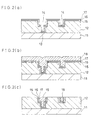
- an insulating layer 12 having a thickness of 0.7 ⁇ m was deposited on a semiconductor substrate 11 having a semiconductor element (not shown) thereon.
- a Ti layer 15 (25 nm) as a resistance reducing layer for reducing the resistance between the semiconductor substrate and a silver layer to be formed later
- a TiN layer 16 (100 nm) as a barrier layer
- a palladium layer 17 (100 nm) as a catalyzer layer for silver plating.
- the semiconductor substrate 11 After the semiconductor substrate 11 had been immersed for 5 hours in the plating bath according to the first embodiment, the semiconductor substrate 11 was washed with water to form a silver layer 18 as shown in Fig. 2 (b).
- the thickness of the silver layer 18 formed by the plating bath was about 0.22 ⁇ m.
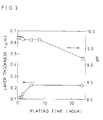
- Fig. 3 shows the relationship between plating time, silver layer thickness and plating bath pH when plating was conducted with the use of the plating bath of the first embodiment.
- the pH shows no substantial change during about 8 hours after the start of plating (reduction of 0.06), and the thickness of the silver layer is saturated to 0.22 ⁇ m (5 hours).
- a plating bath having the same composition as above-mentioned was newly prepared, and the immersion of the semiconductor substrate 11 in the plating bath for 2 hours, was further repeated four times such that silver was embedded in the contact hole 13 and the wiring grooves 14 in their entirety.
- the insulating layer 12 was covered with the silver layer 18 as shown in Fig. 2 (b).
- the embedded wirings 19 contained metallic impurities such as Na, K and the like only in an amount of not greater than the allowable level, no adverse effect was exerted to the characteristics of the semiconductor element. Further, it is noted that both the plating bath of the first embodiment and the characteristics of the palladium layer 17 as the catalyzer layer, provide the embedded wirings 19 with the following three advantages. Firstly, the embedded wirings 19 are improved in finesse or compactness, the adhesion with the semiconductor substrate 11 and embedding characteristics with respect to the contact hole 13 and the wiring grooves 14. Secondly, the embedded wirings 19 are lowered in contact resistance.
- the semiconductor substrate 11 was annealed at 400 to 500°C after the plating process, no void was formed in the embedded wirings 19 and the adhesion between the embedded wirings 19 and the semiconductor substrate 11 did not become defective.
- Such annealing on the semiconductor substrate 11 may be conducted before the silver layer 18 and the like are subjected to chemical mechanical polishing.
- concentrations of the components, the pH, the temperature and the like of the plating bath according to the first embodiment are not limited to those mentioned earlier, but may be set such that silver does not separate out in the plating bath, and that the plating bath is stable from the start of plating to the completion of deposition of a silver layer on the semiconductor substrate.
- the molarity of tartaric acid and ethylenediamine was preferably about 3 times to about 10 times and the molarity of 3,5-diiodotyrosine was preferably 1/300 to 1/30, that the pH was preferably from about 9 to about 12, and that the temperature was preferably from about 20°C to about 50°C. According to the present invention, however, such conditions are not limited to those above-mentioned.
- tungsten or the like may be embedded by CVD only in the contact hole 13 while the silver layer 18 may be embedded only in the wiring grooves 14.
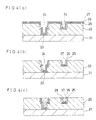
- an insulating layer 22 having a thickness of 0.7 ⁇ m was deposited on a semiconductor substrate 21 having a semiconductor element (not shown) thereon.
- a contact hole (zone which is connected to the semiconductor element) 23 and wiring grooves 24 By a sputtering method, there were deposited a Ti layer 25 (25 nm) as a resistance reducing layer for reducing the resistance between the semiconductor substrate and a silver layer, a TiN layer 26 (100 nm) as a barrier layer, and a palladium layer 27 (100 nm) as a catalyzer layer for silver plating.
- the palladium layer 27, the TiN layer 26 and the Ti layer 25 on the insulating layer 22 were removed by chemical mechanical polishing (CMP).
- the semiconductor substrate 21 After the semiconductor substrate 21 had been immersed for 2 hours in the plating bath according to the first embodiment, the semiconductor substrate 21 was washed with water. Then, a plating bath having the same composition as above-mentioned was newly prepared, and the immersion of the semiconductor substrate 21 in the plating bath for 2 hours, was conducted again such that silver was embedded in the contact hole 23 and the wiring grooves 24 in their entirety. Thus, embedded wirings 28 made of the silver layer were formed as shown in Fig. 4 (c). Silver plating grows only at a portion where the palladium layer 27 as the catalyzer layer is present. Accordingly, silver can selectively be embedded into the contact hole 23 and the wiring grooves 24.
- the embedded wirings 28 contained metallic impurities such as Na, K and the like only in an amount of not greater than the allowable level, no adverse effect was exerted to the characteristics of the semiconductor element. Further, it is noted that both the plating bath of the first embodiment and the characteristics of the palladium layer 27 as the catalyzer layer, provide the embedded wirings 28 with the following three advantages. Firstly, the embedded wirings 28 are improved in finesse or compactness, the adhesion with the semiconductor substrate 21 and embedding characteristics with respect to the contact hole 23 and the wiring grooves 24. Secondly, the embedded wirings 28 are lowered in contact resistance.
- the semiconductor substrate 21 was annealed at 400 to 500°C after the plating process, no void was formed in the embedded wirings 28 and the adhesion between the embedded wirings 28 and the semiconductor substrate 21 did not become defective.
- tungsten or the like may be embedded by CVD only in the contact hole 23 while embedded wirings 28 may be embedded only in the wiring grooves 24.
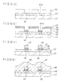
- a first insulating layer 32 was deposited on a semiconductor substrate 31 having a semiconductor element (not shown) thereon. Contact holes were formed in the first insulating layer 32 by a lithography etching technique. A Ti layer and a TiN layer were deposited by a sputtering method, and tungsten was deposited by CVD to form tungsten plugs 33 in the contact holes. Then, there was deposited a second insulating layer 34, on which a resist pattern 35 having openings 35a at wiring zones was formed by a lithography technology.
- the second insulating layer 34 was subjected to etching to form wiring grooves 36 in the second insulating layer 34 as shown in Fig. 5 (b). Then, by collimator sputtering, there were deposited a Ti layer 37 (25 nm) as a resistance reducing layer for reducing the resistance between the semiconductor element and a silver layer, a Tin layer 38 (100 nm) as a barrier layer and a palladium layer 39 (100 nm) as a catalyzer layer for silver plating.
- a Ti layer 37 25 nm
- a Tin layer 38 100 nm
- a palladium layer 39 100 nm
- the resist pattern 35 was removed with a cleaning solution. This caused the Ti layer 37, the Tin layer 38 and the palladium layer 39 on the resist pattern 35 to be lifted off. Thus, the Ti layer 37, the Tin layer 38 and the palladium layer 39 remained only inside of the wiring grooves 36 as shown in Fig. 5 (d).
- the semiconductor substrate 31 After the semiconductor substrate 31 had been immersed for 2 hours in the plating bath according to the first embodiment, the semiconductor substrate 31 was washed with water. Then, a plating bath having the same composition as above-mentioned was newly prepared, and the immersion of the semiconductor substrate 31 in the plating bath for 2 hours, was repeated two times such that silver was embedded in the wiring grooves 36 in their entirety. Thus, embedded wirings 40 made of the silver layer were formed as shown in Fig. 5 (e). Silver plating grows only at a portion where the palladium layer 39 as the catalyzer layer is present. Accordingly, silver can selectively be embedded into the wiring grooves 36.
- the embedded wirings 40 contained metallic impurities such as Na, K and the like only in an amount of not greater than the allowable level, no adverse effect was exerted to the characteristics of the semiconductor element. Further, it is noted that both the plating bath of the first embodiment and the characteristics of the palladium layer 39 as the catalyzer layer, provide the embedded wirings 40 with the following three advantages. Firstly, the embedded wirings 40 are improved in finesse or compactness, the adhesion with the semiconductor substrate 31 and embedding characteristics with respect to the wiring grooves 36. Secondly, the embedded wirings 40 are lowered in contact resistance.
- the semiconductor substrate 31 was annealed at 400 to 500°C after the plating process, no void was formed in the embedded wirings 40 and the adhesion between the embedded wirings 40 and the semiconductor substrate 31 did not become defective.
- a first insulating layer 42 was deposited on a semiconductor substrate 41 having a semiconductor element (not shown) thereon.
- Contact holes were formed in the first insulating layer 42 by a lithography etching technique.
- a Ti layer and a TiN layer were deposited by a sputtering method, and tungsten was deposited by CVD to form tungsten plugs 43 in the contact holes.
- a resist pattern 44 having openings 44a at wiring zones was formed on the first insulating layer 42 by a lithography technology.
- a Ti layer 45 25 nm
- a Tin layer 46 100 nm
- a palladium layer 47 100 nm
- the palladium layer 47, the Tin layer 46 and the Ti layer 45 on the resist pattern 44 were removed by chemical and mechanical polishing (CMP).
- CMP chemical and mechanical polishing
- the semiconductor substrate 41 was washed with water.
- a plating bath having the same composition as above-mentioned was newly prepared, and the immersion of the semiconductor substrate 41 in the plating bath for 2 hours, was repeated two times such that metallic wirings 40 were selectively formed in the openings 44a in the resist pattern 44 (See Fig. 6 (c)).
- Silver plating grows only at a portion where the palladium layer 47 as the catalyzer layer is present. Accordingly, the metallic wirings 40 can selectively be formed only in the wiring zones.
- a second insulating layer 48 as an interlaminar insulating layer was entirely deposited as shown in Fig. 6 (d).
- electroless nickel plating bath having the following composition.
- Nickel sulfate nickel ion source
- reducing agent 2.3 x 10 -1 mol/l
- Lactic acid complexing agent
- Solution of tetramethylammoniumhydroxide pH control agent
- Thiourea stabilizer
- a nickel plated layer having a thickness of 0.3 ⁇ m was deposited on the semiconductor substrate.
- the amounts of Na and K in this nickel plated layer were measured as 0.2 ppm and 0.2 ppm, respectively. These values are much lower than the allowable level for metallic impurities contained in a wiring metal of a semiconductor device. Thus, it was made sure that the nickel layer deposited with the use of this plating bath can be used for a metallic wiring of a semiconductor device.
- an insulating layer 52 was deposited on a semiconductor substrate 51 having a semiconductor element (not shown) thereon.
- a lithography and etching technique there were formed contact holes in the insulating layer 52.
- a Ti layer 53 25 nm
- a TiN layer 54 100 nm
- a palladium layer 55 100 nm
- the palladium layer 55, the Tin layer 54 and the Ti layer 53 on the insulating layer 52 were removed by chemical mechanical polishing (CMP).
- the semiconductor substrate 51 After the semiconductor substrate 51 had been immersed for 1 hours in the plating bath according to the second embodiment, the semiconductor substrate 51 was washed with water. Thus, nickel was entirely embedded in the contract holes to form embedded plugs 56 made of a nickel layer as shown in Fig. 7 (c). Nickel plating grows only at a portion where the palladium layer 55 as the catalyzer layer is present. Accordingly, nickel can selectively be embedded in the contact holes.
- the embedded plugs 56 contained metallic impurities such as Na, K and the like only in an amount of not greater than the allowable level, no adverse effect was exerted to the characteristics of the semiconductor element. Further, it is noted that both the plating bath of the third embodiment and the characteristics of the palladium layer 55 as the catalyzer layer, provide the embedded plugs 56 with the following three advantages. Firstly, the embedded plugs 56 are improved in finesse or compactness, the adhesion with the semiconductor substrate 51 and embedding characteristics with respect to the contact holes. Secondly, the embedded plugs 56 are lowered in contact resistance.
- the semiconductor substrate 51 was annealed at 400 to 500°C after the plating process, no void was formed in the embedded plugs 56 and the adhesion between the embedded plugs 56 and the semiconductor substrate 51 did not become defective.
- the concentrations of the components, the pH, the temperature and the like of the plating bath according to the second embodiment, are not limited to those mentioned earlier, but may be set such that nickel does not separate out in the plating bath, and that the plating bath is stable from the start of plating to the completion of deposition of a nickel layer on the semiconductor substrate.
- the molarity of nickel nitrate the molarity of hypophosphorous acid and lactic acid was preferably about 2 times to about 10 times and the molarity of thiourea was preferably 1/50000 to 1/10000, that the pH was preferably from about 3.5 to about 6, and that the temperature was preferably from about 80°C to about 100°C. According to the present invention, however, such conditions are not limited to those above-mentioned.
- the plating bath according to the first embodiment was used in each of the first to fourth wiring forming methods, and the plating bath according to the second embodiment was used in the fifth wiring forming method.
- the embedded wirings or embedded plugs are different in material from the layer thereunder. Accordingly, the resistance reducing layer, the barrier layer and the catalyzer layer are formed. However, when the embedded wirings or embedded plugs are the same in material as the layer thereunder, such resistance reducing layer, barrier layer and catalyzer layer may not be formed.
Landscapes
- Chemical & Material Sciences (AREA)
- General Chemical & Material Sciences (AREA)
- Chemical Kinetics & Catalysis (AREA)
- Engineering & Computer Science (AREA)
- Materials Engineering (AREA)
- Mechanical Engineering (AREA)
- Metallurgy (AREA)
- Organic Chemistry (AREA)
- Electrodes Of Semiconductors (AREA)
- Chemically Coating (AREA)
- Internal Circuitry In Semiconductor Integrated Circuit Devices (AREA)
Description
| Silver nitrate (silver ion source) | 8 x 10⁻³ mol/l |
| Rochelle salt (reducing agent) | 3.5 x 10⁻² mol/l |
| Ethylenediamine (complexing agent) | 5.4 x 10⁻² mol/l |
| 3,5-Diiodotyrosine (stabilizer) | 4.0 x 10⁻⁵ mol/l |
| NaOH or KOH (pH control agent) | |
| pH | 10.0 |
| | 35°C |
| Silver nitrate (silver ion source) | 8.8 x 10⁻³ mol/l |
| Tartaric acid (reducing agent) | 5.3 x 10⁻² mol/l |
| Ethylenediamine (complexing agent) | 5.4 x 10⁻² mol/l |
| 15-wt% Solution of tetramethylammoniumhydroxide (pH control agent) | |
| 3,5-Diiodotyrosine (stabilizer) | 8.0 x 10⁻⁵ mol/l |
| pH | 10.0 |
| | 35°C |
| Nickel sulfate (nickel ion source) | 8.0 x 10⁻² mol/l |
| Hypophosphorous acid (reducing agent) | 2.3 x 10⁻¹ mol/l |
| Lactic acid (complexing agent) | 3.0 x 10⁻¹ mol/l |
| 15-wt% Solution of tetramethylammoniumhydroxide (pH control agent) | |
| Thiourea (stabilizer) | 5.0 x 10⁻⁶ mol/l |
| pH | 4.5 |
| Bath temperature | 90°C |
Claims (29)
- Use of an electroless plating bath, comprisinga metallic material containing metallic ions,a reducing agent for said metallic ions which contains no metala complexing agent for said metallic ions which contains no metal, anda pH control agent which contains no metal,for forming a wiring of a semiconductor device.
- Use of claim 1 characterized in that said metallic ions are silver ions, copper ions, gold ions, nickel ions, cobalt ions or palladium ions.
- Use of claim 1 characterized in that said metallic ions are silver ions, copper ions, gold ions or palladium ions, and said reducing agent comprises at least one substance selected from the group consisting of tartaric acid, tartrate, monosaccharide, disaccharide, polysaccharide, hydrazine, a hydrazine derivative, aldehyde and polyol.
- Use of claim 1 characterized in that said metallic ions are nickel ions, or cobalt ions, and said reducing agent comprises at least one substance selected from the group consisting of hypophosphorous acid, hypophosphite, a boron hydroxide compound hydrazine and a hydrazine derivative.
- Use of claim 1 characterized in that said metallic ions are silver ions or copper ions, and said complexing agent comprises at least one substance selected from the group consisting of ethylenediamine, an ethylenediamine derivative, ammonia and triethanolamine.
- Use of claim 1 characterized in that said metallic ions are gold ions, nickel ions, cobalt ions or palladium ions, and said complexing agent is a compound containing a carboxylic acid group.
- Use of claim 1 characterized in that said pH control agent comprises at least one substance selected from the group consisting of ammonium salt, ammonia, nitric acid and boric acid.
- Use of claim 1 characterized in that the electroless plating bath further contains at least one substance selected from the group consisting of:a pH buffer for restraining the plating solution being lowered and pH, said buffer containing no metal;a promoter for restraining the plating speed from being lowered, said promoter containing no metal;a stabilizer for preventing said plating solution from being decomposed, said stabilizer containing no metal;and a surfactant for making the resulting plated layer fine in quality, said surfactant containing no metal.
- A method of forming a wiring of a semiconductor device, comprising:the first step of forming a concave at a contact zone or a wiring zone of a resist pattern or an insulating layer formed on the semiconductor substrate; andthe second step of forming an embedded metallic layer in said concave with the use of an electroless plating bath comprising: a metallic material containing metallic ions; a reducing agent for said metallic ions which contains no metal a complexing agent for said metallic ions which contains no metal;and a pH control agent which contains no metal.
- A method of forming a wiring of a semiconductor device according to Claim 9, further comprising, between said first and second steps, the intermediate layer forming step of successively forming, on the bottom of said concave, a resistance reducing layer for reducing the contact resistance of said embedded metallic layer, a barrier layer for preventing said embedded metallic layer from reacting, and a catalyzer layer for promoting the reaction of said metallic ions.
- A method of forming a wiring of a semiconductor device according to Claim 10, whereinsaid intermediate layer forming step comprises: the step of successively forming, inside of said concave and on said resist pattern or said insulating layer, said resistance reducing layer, said barrier layer and said catalyzer layer; and the step of removing, by a chemical and mechanical polishing method, said resistance reducing layer, said barrier layer and said catalyzer layer on said resist pattern or said insulating layer such that said resistance reducing layer, said barrier layer and said catalyzer layer are formed only on said bottom of said concave, andsaid second step comprises the step of selectively forming said embedded metallic layer on said catalyzer layer formed only on said bottom of said concave.
- A method of forming a wiring of a semiconductor device according to Claim 9, wherein said catalyzer layer is a Pd layer or a Ti layer.
- A method of forming a wiring of a semiconductor device according to Claim 9, wherein said barrier layer is a TiN layer, a TiW layer or a W layer.
- A method of forming a wiring of a semiconductor device according to Claim 9, wherein said resistance reducing layer is a Ti layer.
- A method of forming a wiring of a semiconductor device according to Claim 9, wherein said second step comprises: the step of forming, with the use of said electroless plating bath, a metallic layer inside of said concave and on said resist pattern or said insulating layer in its entirety; and the step of removing said metallic layer on said resist pattern or said insulating layer such that said embedded metallic layer is formed inside of said concave.
- A method of forming a wiring of a semiconductor device according to Claim 9, wherein said second step comprises: the step of forming, with the use of said electroless plating bath, a metallic layer inside of said concave and on said insulating layer in its entirety; and the step of removing, by a chemical and mechanical polishing method, said metallic layer on said insulating layer such that said embedded metallic layer is formed inside of said concave with the surface of said embedded metallic layer being flush with the surface of said insulating layer.
- A method of forming a wiring of a semiconductor device according to Claim 9,further comprising, before said first step, the lower insulating layer forming step of forming, on said semiconductor substrate, a lower insulating layer having an embedded plug, and whereinsaid first step comprises:the step of forming said insulating layer on said lower insulating layer;the step of forming, on said insulating layer, a wiring zone forming resist pattern having an opening at the position thereof corresponding to said embedded plug; andthe step of etching said insulating layer with said wiring zone forming resist pattern serving as a mask, thereby to form, in said insulating layer, said concave which will result in a wiring zone.
- A method of forming a wiring of a semiconductor device according to Claim 9,further comprising, before said first step, the lower insulating layer forming step of forming, on said semiconductor substrate, a lower insulating layer having an embedded plug, and whereinsaid first step comprises the step of forming, on said lower insulating layer, said resist pattern having, at the position thereof corresponding to said embedded plug, an opening which will result in said concave.
- A method of forming a wiring of a semiconductor device according to Claim 9, wherein said metallic ions of said electroless plating bath are silver ions, copper ions, gold ions, nickel ions, cobalt ions or palladium ions.
- A method of forming a wiring of a semiconductor device according to Claim 9, whereinsaid metallic ions of said electroless plating bath are silver ions, copper ions, gold ions or palladium ions, andsaid reducing agent for said electroless plating bath comprises at least one substance selected from the group consisting of tartaric acid, tartrate, monosaccharide, disaccharide, polysaccharide, hydrazine, a hydrazine derivative, aldehyde and polyol.
- A method of forming a wiring of a semiconductor device according to Claim 9, whereinsaid metallic ions of said electroless plating bath are nickel ions or cobalt ions, andsaid reducing agent for said electroless plating bath comprises at least one substance selected from the group consisting of hypophosphorous acid, hypophosphite a boron hydroxide compound hydrazine and a hydrazine derivative.
- A method of forming a wiring of a semiconductor device according to Claim 9, whereinsaid metallic ions of said electroless plating bath are silver ions or copper ions, andsaid complexing agent for said electroless plating bath comprises at least one substance selected from the group consisting of ethylenediamine, an ethylenediamine derivative, ammonia and triethanolamine.
- A method of forming a wiring of a semiconductor device according to Claim 9, whereinsaid metallic ions of said electroless plating bath are gold ions, nickel ions, cobalt ions or palladium ions, andsaid complexing agent for said electroless plating bath is a compound containing a carboxylic acid group.
- A method of forming a wiring of a semiconductor device according to Claim 9, wherein said pH control agent of said electroless plating bath comprises at least one substance selected from the group consisting of ammonium salt, ammonia, nitric acid and boric acid.
- A method of forming a wiring of a semiconductor device according to Claim 9, wherein said metallic material of said electroless plating bath is silver nitrate, said reducing agent of said electroless plating bath is tartaric acid, said complexing agent of said electroless plating bath is ethylenediamine, and said pH control agent of said electroless plating bath is tetramethylammoniumhydroxide.
- A method of forming a wiring of a semiconductor device according to Claim 9, wherein said metallic material of said electroless plating bath comprises two or more types of metallic ions.
- A method of forming a wiring of a semiconductor device according to Claim 9, wherein said electroless plating bath further comprises at least one substance selected from the group consisting of: a pH buffer for restraining the plating solution from being lowered in pH, said buffer containing no metal; a promotor for restraining the plating speed from being lowered, said promotor containing no metal; a stablizer for preventing said plating solution from being decomposed, said stabilizer containing no metal; and a surfactant for making the resulting plated layer fine in quality, said surfactant containing no metal.
- An electroless plating bath comprising:a metallic material containing metallic ions,a reducing agent for said metallic ions which contains no metal,a complexing agent for said metallic ions which contains no metal,and a pH control agent which contains no metal, characterized in that said metallic material is silver nitrate, said reducing agent is tartaric acid, said complexing agent is ethylenediamine, and said pH control agent is tetramethylammoniumhydroxide.
- An electroless plating bath comprising:characterized in that said metallic material comprises two or more types of metallic ions.a metallic material containing metallic ions,a reducing agent of said metallic ions which contains no metal,a complexing agent of said metallic ions which contains no metal,and a pH control agent which contains no metal,
Applications Claiming Priority (2)
| Application Number | Priority Date | Filing Date | Title |
|---|---|---|---|
| JP16203094 | 1994-07-14 | ||
| JP162030/94 | 1994-07-14 |
Publications (2)
| Publication Number | Publication Date |
|---|---|
| EP0692554A1 EP0692554A1 (en) | 1996-01-17 |
| EP0692554B1 true EP0692554B1 (en) | 1999-01-20 |
Family
ID=15746747
Family Applications (1)
| Application Number | Title | Priority Date | Filing Date |
|---|---|---|---|
| EP95110948A Expired - Lifetime EP0692554B1 (en) | 1994-07-14 | 1995-07-12 | Electroless plating bath used for forming a wiring of a semiconductor device, and method of forming a wiring of a semiconductor device |
Country Status (4)
| Country | Link |
|---|---|
| US (2) | US5645628A (en) |
| EP (1) | EP0692554B1 (en) |
| KR (1) | KR960005765A (en) |
| DE (1) | DE69507389T2 (en) |
Cited By (1)
| Publication number | Priority date | Publication date | Assignee | Title |
|---|---|---|---|---|
| WO2003098681A1 (en) * | 2002-05-16 | 2003-11-27 | National University Of Singapore | Wafer level electroless copper metallization and bumping process, and plating solutions for semiconductor wafer and microchip |
Families Citing this family (149)
| Publication number | Priority date | Publication date | Assignee | Title |
|---|---|---|---|---|
| JP3737221B2 (en) * | 1996-09-06 | 2006-01-18 | 英樹 松村 | Thin film forming method and thin film forming apparatus |
| US6896826B2 (en) * | 1997-01-09 | 2005-05-24 | Advanced Technology Materials, Inc. | Aqueous cleaning composition containing copper-specific corrosion inhibitor for cleaning inorganic residues on semiconductor substrate |
| US6331239B1 (en) | 1997-04-07 | 2001-12-18 | Okuno Chemical Industries Co., Ltd. | Method of electroplating non-conductive plastic molded products |
| TW337606B (en) * | 1997-07-18 | 1998-08-01 | Winbond Electronics Corp | Process for forming plugs by chemical mechanical polishing |
| DE19733991A1 (en) * | 1997-08-06 | 1999-02-11 | Doduco Gmbh | Reductive Ni bath |
| US6110011A (en) | 1997-11-10 | 2000-08-29 | Applied Materials, Inc. | Integrated electrodeposition and chemical-mechanical polishing tool |
| US6406939B1 (en) | 1998-05-02 | 2002-06-18 | Charles W. C. Lin | Flip chip assembly with via interconnection |
| SG75841A1 (en) | 1998-05-02 | 2000-10-24 | Eriston Invest Pte Ltd | Flip chip assembly with via interconnection |
| KR100635685B1 (en) | 1998-05-25 | 2006-10-17 | 가부시키가이샤 히타치세이사쿠쇼 | Semiconductor device and manufacturing method |
| US6100194A (en) * | 1998-06-22 | 2000-08-08 | Stmicroelectronics, Inc. | Silver metallization by damascene method |
| US6436816B1 (en) * | 1998-07-31 | 2002-08-20 | Industrial Technology Research Institute | Method of electroless plating copper on nitride barrier |
| JP3187011B2 (en) * | 1998-08-31 | 2001-07-11 | 日本電気株式会社 | Method for manufacturing semiconductor device |
| US6140239A (en) * | 1998-11-25 | 2000-10-31 | Advanced Micro Devices, Inc. | Chemically removable Cu CMP slurry abrasive |
| US6627553B1 (en) * | 1998-11-27 | 2003-09-30 | Showa Denko K.K. | Composition for removing side wall and method of removing side wall |
| SG78324A1 (en) | 1998-12-17 | 2001-02-20 | Eriston Technologies Pte Ltd | Bumpless flip chip assembly with strips-in-via and plating |
| SG82591A1 (en) | 1998-12-17 | 2001-08-21 | Eriston Technologies Pte Ltd | Bumpless flip chip assembly with solder via |
| TW444236B (en) | 1998-12-17 | 2001-07-01 | Charles Wen Chyang Lin | Bumpless flip chip assembly with strips and via-fill |
| US6383269B1 (en) * | 1999-01-27 | 2002-05-07 | Shipley Company, L.L.C. | Electroless gold plating solution and process |
| JP3352422B2 (en) * | 1999-02-10 | 2002-12-03 | セントラル硝子株式会社 | Chemical solution for forming silver film and method for forming silver film |
| KR20020019056A (en) * | 1999-06-01 | 2002-03-09 | 히가시 데쓰로 | Method of manufacturing semiconductor device and manufacturing apparatus |
| JP2001107258A (en) * | 1999-10-06 | 2001-04-17 | Hitachi Ltd | Electroless copper plating method and plating apparatus and multilayer wiring board |
| US20020039839A1 (en) * | 1999-12-14 | 2002-04-04 | Thomas Terence M. | Polishing compositions for noble metals |
| JP2001181854A (en) * | 1999-12-22 | 2001-07-03 | Ebara Corp | Electroless plating solution and wiring forming method using the same |
| KR100758186B1 (en) * | 2000-03-21 | 2007-09-13 | 와코 쥰야꾸 고교 가부시키가이샤 | Semiconductor Substrate Cleaner and Cleaning Method |
| JP3444276B2 (en) * | 2000-06-19 | 2003-09-08 | 株式会社村田製作所 | Electroless copper plating bath, electroless copper plating method and electronic component |
| US6387542B1 (en) * | 2000-07-06 | 2002-05-14 | Honeywell International Inc. | Electroless silver plating |
| US6991675B2 (en) * | 2000-08-21 | 2006-01-31 | Shipley Company, L.L.C. | Electroless displacement gold plating solution and additive for use in preparing plating solution |
| US6562657B1 (en) | 2000-08-22 | 2003-05-13 | Charles W. C. Lin | Semiconductor chip assembly with simultaneously electrolessly plated contact terminal and connection joint |
| US6350633B1 (en) | 2000-08-22 | 2002-02-26 | Charles W. C. Lin | Semiconductor chip assembly with simultaneously electroplated contact terminal and connection joint |
| US6551861B1 (en) | 2000-08-22 | 2003-04-22 | Charles W. C. Lin | Method of making a semiconductor chip assembly by joining the chip to a support circuit with an adhesive |
| US6403460B1 (en) | 2000-08-22 | 2002-06-11 | Charles W. C. Lin | Method of making a semiconductor chip assembly |
| US6660626B1 (en) | 2000-08-22 | 2003-12-09 | Charles W. C. Lin | Semiconductor chip assembly with simultaneously electrolessly plated contact terminal and connection joint |
| US6436734B1 (en) | 2000-08-22 | 2002-08-20 | Charles W. C. Lin | Method of making a support circuit for a semiconductor chip assembly |
| US6402970B1 (en) | 2000-08-22 | 2002-06-11 | Charles W. C. Lin | Method of making a support circuit for a semiconductor chip assembly |
| US6562709B1 (en) | 2000-08-22 | 2003-05-13 | Charles W. C. Lin | Semiconductor chip assembly with simultaneously electroplated contact terminal and connection joint |
| US6350386B1 (en) | 2000-09-20 | 2002-02-26 | Charles W. C. Lin | Method of making a support circuit with a tapered through-hole for a semiconductor chip assembly |
| US6511865B1 (en) | 2000-09-20 | 2003-01-28 | Charles W. C. Lin | Method for forming a ball bond connection joint on a conductive trace and conductive pad in a semiconductor chip assembly |
| US6350632B1 (en) | 2000-09-20 | 2002-02-26 | Charles W. C. Lin | Semiconductor chip assembly with ball bond connection joint |
| US6544813B1 (en) | 2000-10-02 | 2003-04-08 | Charles W. C. Lin | Method of making a semiconductor chip assembly with a conductive trace subtractively formed before and after chip attachment |
| US6448108B1 (en) | 2000-10-02 | 2002-09-10 | Charles W. C. Lin | Method of making a semiconductor chip assembly with a conductive trace subtractively formed before and after chip attachment |
| US7071089B1 (en) | 2000-10-13 | 2006-07-04 | Bridge Semiconductor Corporation | Method of making a semiconductor chip assembly with a carved bumped terminal |
| US6667229B1 (en) | 2000-10-13 | 2003-12-23 | Bridge Semiconductor Corporation | Method of connecting a bumped compliant conductive trace and an insulative base to a semiconductor chip |
| US7129575B1 (en) | 2000-10-13 | 2006-10-31 | Bridge Semiconductor Corporation | Semiconductor chip assembly with bumped metal pillar |
| US7190080B1 (en) | 2000-10-13 | 2007-03-13 | Bridge Semiconductor Corporation | Semiconductor chip assembly with embedded metal pillar |
| US7264991B1 (en) | 2000-10-13 | 2007-09-04 | Bridge Semiconductor Corporation | Method of connecting a conductive trace to a semiconductor chip using conductive adhesive |
| US6537851B1 (en) | 2000-10-13 | 2003-03-25 | Bridge Semiconductor Corporation | Method of connecting a bumped compliant conductive trace to a semiconductor chip |
| US6872591B1 (en) | 2000-10-13 | 2005-03-29 | Bridge Semiconductor Corporation | Method of making a semiconductor chip assembly with a conductive trace and a substrate |
| US7262082B1 (en) | 2000-10-13 | 2007-08-28 | Bridge Semiconductor Corporation | Method of making a three-dimensional stacked semiconductor package with a metal pillar and a conductive interconnect in an encapsulant aperture |
| US6949408B1 (en) | 2000-10-13 | 2005-09-27 | Bridge Semiconductor Corporation | Method of connecting a conductive trace and an insulative base to a semiconductor chip using multiple etch steps |
| US6984576B1 (en) | 2000-10-13 | 2006-01-10 | Bridge Semiconductor Corporation | Method of connecting an additively and subtractively formed conductive trace and an insulative base to a semiconductor chip |
| US7129113B1 (en) | 2000-10-13 | 2006-10-31 | Bridge Semiconductor Corporation | Method of making a three-dimensional stacked semiconductor package with a metal pillar in an encapsulant aperture |
| US6908788B1 (en) | 2000-10-13 | 2005-06-21 | Bridge Semiconductor Corporation | Method of connecting a conductive trace to a semiconductor chip using a metal base |
| US6673710B1 (en) | 2000-10-13 | 2004-01-06 | Bridge Semiconductor Corporation | Method of connecting a conductive trace and an insulative base to a semiconductor chip |
| US6440835B1 (en) | 2000-10-13 | 2002-08-27 | Charles W. C. Lin | Method of connecting a conductive trace to a semiconductor chip |
| US6576493B1 (en) | 2000-10-13 | 2003-06-10 | Bridge Semiconductor Corporation | Method of connecting a conductive trace and an insulative base to a semiconductor chip using multiple etch steps |
| US6876072B1 (en) | 2000-10-13 | 2005-04-05 | Bridge Semiconductor Corporation | Semiconductor chip assembly with chip in substrate cavity |
| US6492252B1 (en) | 2000-10-13 | 2002-12-10 | Bridge Semiconductor Corporation | Method of connecting a bumped conductive trace to a semiconductor chip |
| US7319265B1 (en) | 2000-10-13 | 2008-01-15 | Bridge Semiconductor Corporation | Semiconductor chip assembly with precision-formed metal pillar |
| US6548393B1 (en) | 2000-10-13 | 2003-04-15 | Charles W. C. Lin | Semiconductor chip assembly with hardened connection joint |
| US7075186B1 (en) | 2000-10-13 | 2006-07-11 | Bridge Semiconductor Corporation | Semiconductor chip assembly with interlocked contact terminal |
| US6740576B1 (en) | 2000-10-13 | 2004-05-25 | Bridge Semiconductor Corporation | Method of making a contact terminal with a plated metal peripheral sidewall portion for a semiconductor chip assembly |
| US6576539B1 (en) | 2000-10-13 | 2003-06-10 | Charles W.C. Lin | Semiconductor chip assembly with interlocked conductive trace |
| US7094676B1 (en) | 2000-10-13 | 2006-08-22 | Bridge Semiconductor Corporation | Semiconductor chip assembly with embedded metal pillar |
| US7414319B2 (en) * | 2000-10-13 | 2008-08-19 | Bridge Semiconductor Corporation | Semiconductor chip assembly with metal containment wall and solder terminal |
| US7132741B1 (en) | 2000-10-13 | 2006-11-07 | Bridge Semiconductor Corporation | Semiconductor chip assembly with carved bumped terminal |
| US7009297B1 (en) | 2000-10-13 | 2006-03-07 | Bridge Semiconductor Corporation | Semiconductor chip assembly with embedded metal particle |
| US6699780B1 (en) | 2000-10-13 | 2004-03-02 | Bridge Semiconductor Corporation | Method of connecting a conductive trace to a semiconductor chip using plasma undercut etching |
| US6444489B1 (en) | 2000-12-15 | 2002-09-03 | Charles W. C. Lin | Semiconductor chip assembly with bumped molded substrate |
| US6653170B1 (en) | 2001-02-06 | 2003-11-25 | Charles W. C. Lin | Semiconductor chip assembly with elongated wire ball bonded to chip and electrolessly plated to support circuit |
| JP2002348680A (en) * | 2001-05-22 | 2002-12-04 | Sharp Corp | Metal film pattern and method of manufacturing the same |
| US6645557B2 (en) | 2001-10-17 | 2003-11-11 | Atotech Deutschland Gmbh | Metallization of non-conductive surfaces with silver catalyst and electroless metal compositions |
| US6645567B2 (en) * | 2001-12-19 | 2003-11-11 | Intel Corporation | Electroless plating bath composition and method of using |
| KR100438673B1 (en) * | 2001-12-29 | 2004-07-03 | 주식회사 하이닉스반도체 | Method for fabricating capacitor |
| US6604987B1 (en) * | 2002-06-06 | 2003-08-12 | Cabot Microelectronics Corporation | CMP compositions containing silver salts |
| US20040040852A1 (en) * | 2002-08-30 | 2004-03-04 | Shipley Company, L.L.C. | Plating method |
| US20040043159A1 (en) * | 2002-08-30 | 2004-03-04 | Shipley Company, L.L.C. | Plating method |
| JP4294589B2 (en) * | 2002-09-11 | 2009-07-15 | エスペック株式会社 | Electroless plating solution, electroless plating method and electroless plating object using the same |
| US6897152B2 (en) * | 2003-02-05 | 2005-05-24 | Enthone Inc. | Copper bath composition for electroless and/or electrolytic filling of vias and trenches for integrated circuit fabrication |
| TWI251920B (en) * | 2003-10-17 | 2006-03-21 | Phoenix Prec Technology Corp | Circuit barrier structure of semiconductor package substrate and method for fabricating the same |
| US7993983B1 (en) | 2003-11-17 | 2011-08-09 | Bridge Semiconductor Corporation | Method of making a semiconductor chip assembly with chip and encapsulant grinding |
| US7538415B1 (en) | 2003-11-20 | 2009-05-26 | Bridge Semiconductor Corporation | Semiconductor chip assembly with bumped terminal, filler and insulative base |
| US7425759B1 (en) | 2003-11-20 | 2008-09-16 | Bridge Semiconductor Corporation | Semiconductor chip assembly with bumped terminal and filler |
| US20070111167A1 (en) | 2004-02-11 | 2007-05-17 | Colgate-Palmolive Company | Light-based toothbrush |
| US20050175956A1 (en) * | 2004-02-11 | 2005-08-11 | Russell Bruce M. | Toothbrush for whitening teeth |
| US6933231B1 (en) * | 2004-06-28 | 2005-08-23 | Micron Technology, Inc. | Methods of forming conductive interconnects, and methods of depositing nickel |
| US20060029833A1 (en) * | 2004-08-09 | 2006-02-09 | Ivanov Igor C | Methods for forming a barrier layer with periodic concentrations of elements and structures resulting therefrom |
| US7268421B1 (en) | 2004-11-10 | 2007-09-11 | Bridge Semiconductor Corporation | Semiconductor chip assembly with welded metal pillar that includes enlarged ball bond |
| US7446419B1 (en) | 2004-11-10 | 2008-11-04 | Bridge Semiconductor Corporation | Semiconductor chip assembly with welded metal pillar of stacked metal balls |
| US7750483B1 (en) | 2004-11-10 | 2010-07-06 | Bridge Semiconductor Corporation | Semiconductor chip assembly with welded metal pillar and enlarged plated contact terminal |
| US7767009B2 (en) | 2005-09-14 | 2010-08-03 | OMG Electronic Chemicals, Inc. | Solution and process for improving the solderability of a metal surface |
| US7410899B2 (en) * | 2005-09-20 | 2008-08-12 | Enthone, Inc. | Defectivity and process control of electroless deposition in microelectronics applications |
| JP4844716B2 (en) * | 2005-09-27 | 2011-12-28 | 上村工業株式会社 | Electroless palladium plating bath |
| KR100859259B1 (en) * | 2005-12-29 | 2008-09-18 | 주식회사 엘지화학 | Cobalt-based alloy electroless plating solution for cap layer formation and electroless plating method using the same |
| EP1876260B1 (en) * | 2006-07-07 | 2018-11-28 | Rohm and Haas Electronic Materials LLC | Improved electroless copper compositions |
| KR100815376B1 (en) * | 2006-08-17 | 2008-03-19 | 삼성전자주식회사 | Novel metal pattern manufacturing method and flat panel display device using same |
| US7494843B1 (en) | 2006-12-26 | 2009-02-24 | Bridge Semiconductor Corporation | Method of making a semiconductor chip assembly with thermal conductor and encapsulant grinding |
| US7811863B1 (en) | 2006-10-26 | 2010-10-12 | Bridge Semiconductor Corporation | Method of making a semiconductor chip assembly with metal pillar and encapsulant grinding and heat sink attachment |
| HK1093002A2 (en) * | 2006-11-16 | 2007-02-16 | 方景礼 | Alkalescent chemical silver plating solution |
| JP2009228078A (en) * | 2008-03-24 | 2009-10-08 | Fujitsu Ltd | Electroplating liquid, electroplating method and method of manufacturing semiconductor device |
| US8282667B2 (en) | 2009-06-05 | 2012-10-09 | Entellus Medical, Inc. | Sinus dilation catheter |
| US8946046B1 (en) | 2012-05-02 | 2015-02-03 | Crossbar, Inc. | Guided path for forming a conductive filament in RRAM |
| US9601692B1 (en) | 2010-07-13 | 2017-03-21 | Crossbar, Inc. | Hetero-switching layer in a RRAM device and method |
| US9570678B1 (en) | 2010-06-08 | 2017-02-14 | Crossbar, Inc. | Resistive RAM with preferental filament formation region and methods |
| US9012307B2 (en) | 2010-07-13 | 2015-04-21 | Crossbar, Inc. | Two terminal resistive switching device structure and method of fabricating |
| CN103081093B (en) | 2010-06-11 | 2015-06-03 | 科洛斯巴股份有限公司 | Pillar structure and method of memory device |
| US8374018B2 (en) | 2010-07-09 | 2013-02-12 | Crossbar, Inc. | Resistive memory using SiGe material |
| US8168506B2 (en) | 2010-07-13 | 2012-05-01 | Crossbar, Inc. | On/off ratio for non-volatile memory device and method |
| US8569172B1 (en) | 2012-08-14 | 2013-10-29 | Crossbar, Inc. | Noble metal/non-noble metal electrode for RRAM applications |
| US8884261B2 (en) | 2010-08-23 | 2014-11-11 | Crossbar, Inc. | Device switching using layered device structure |
| US8947908B2 (en) | 2010-11-04 | 2015-02-03 | Crossbar, Inc. | Hetero-switching layer in a RRAM device and method |
| US8492195B2 (en) | 2010-08-23 | 2013-07-23 | Crossbar, Inc. | Method for forming stackable non-volatile resistive switching memory devices |
| US9401475B1 (en) * | 2010-08-23 | 2016-07-26 | Crossbar, Inc. | Method for silver deposition for a non-volatile memory device |
| US8889521B1 (en) * | 2012-09-14 | 2014-11-18 | Crossbar, Inc. | Method for silver deposition for a non-volatile memory device |
| US8558212B2 (en) | 2010-09-29 | 2013-10-15 | Crossbar, Inc. | Conductive path in switching material in a resistive random access memory device and control |
| US8391049B2 (en) | 2010-09-29 | 2013-03-05 | Crossbar, Inc. | Resistor structure for a non-volatile memory device and method |
| US8502185B2 (en) | 2011-05-31 | 2013-08-06 | Crossbar, Inc. | Switching device having a non-linear element |
| USRE46335E1 (en) | 2010-11-04 | 2017-03-07 | Crossbar, Inc. | Switching device having a non-linear element |
| US9153623B1 (en) | 2010-12-31 | 2015-10-06 | Crossbar, Inc. | Thin film transistor steering element for a non-volatile memory device |
| US9620206B2 (en) | 2011-05-31 | 2017-04-11 | Crossbar, Inc. | Memory array architecture with two-terminal memory cells |
| US8619459B1 (en) | 2011-06-23 | 2013-12-31 | Crossbar, Inc. | High operating speed resistive random access memory |
| US9486614B2 (en) | 2011-06-29 | 2016-11-08 | Entellus Medical, Inc. | Sinus dilation catheter |
| US9564587B1 (en) | 2011-06-30 | 2017-02-07 | Crossbar, Inc. | Three-dimensional two-terminal memory with enhanced electric field and segmented interconnects |
| US8946669B1 (en) | 2012-04-05 | 2015-02-03 | Crossbar, Inc. | Resistive memory device and fabrication methods |
| US9166163B2 (en) | 2011-06-30 | 2015-10-20 | Crossbar, Inc. | Sub-oxide interface layer for two-terminal memory |
| US9627443B2 (en) | 2011-06-30 | 2017-04-18 | Crossbar, Inc. | Three-dimensional oblique two-terminal memory with enhanced electric field |
| CN103828047A (en) | 2011-07-22 | 2014-05-28 | 科洛斯巴股份有限公司 | Seed layer for a p + silicon germanium material for non-volatile memory device and method |
| US9729155B2 (en) | 2011-07-29 | 2017-08-08 | Crossbar, Inc. | Field programmable gate array utilizing two-terminal non-volatile memory |
| US10056907B1 (en) | 2011-07-29 | 2018-08-21 | Crossbar, Inc. | Field programmable gate array utilizing two-terminal non-volatile memory |
| US8674724B2 (en) | 2011-07-29 | 2014-03-18 | Crossbar, Inc. | Field programmable gate array utilizing two-terminal non-volatile memory |
| US9283360B2 (en) | 2011-11-10 | 2016-03-15 | Entellus Medical, Inc. | Methods and devices for treating sinusitis |
| US9685608B2 (en) | 2012-04-13 | 2017-06-20 | Crossbar, Inc. | Reduced diffusion in metal electrode for two-terminal memory |
| US8658476B1 (en) | 2012-04-20 | 2014-02-25 | Crossbar, Inc. | Low temperature P+ polycrystalline silicon material for non-volatile memory device |
| US8796658B1 (en) | 2012-05-07 | 2014-08-05 | Crossbar, Inc. | Filamentary based non-volatile resistive memory device and method |
| US8765566B2 (en) | 2012-05-10 | 2014-07-01 | Crossbar, Inc. | Line and space architecture for a non-volatile memory device |
| US9583701B1 (en) | 2012-08-14 | 2017-02-28 | Crossbar, Inc. | Methods for fabricating resistive memory device switching material using ion implantation |
| US10096653B2 (en) | 2012-08-14 | 2018-10-09 | Crossbar, Inc. | Monolithically integrated resistive memory using integrated-circuit foundry compatible processes |
| US9312483B2 (en) | 2012-09-24 | 2016-04-12 | Crossbar, Inc. | Electrode structure for a non-volatile memory device and method |
| US9576616B2 (en) | 2012-10-10 | 2017-02-21 | Crossbar, Inc. | Non-volatile memory with overwrite capability and low write amplification |
| US11068620B2 (en) | 2012-11-09 | 2021-07-20 | Crossbar, Inc. | Secure circuit integrated with memory layer |
| US8982647B2 (en) | 2012-11-14 | 2015-03-17 | Crossbar, Inc. | Resistive random access memory equalization and sensing |
| US9412790B1 (en) | 2012-12-04 | 2016-08-09 | Crossbar, Inc. | Scalable RRAM device architecture for a non-volatile memory device and method |
| US10036097B2 (en) | 2012-12-21 | 2018-07-31 | Okuno Chemical Industries Co., Ltd. | Conductive coating film forming bath |
| US9406379B2 (en) | 2013-01-03 | 2016-08-02 | Crossbar, Inc. | Resistive random access memory with non-linear current-voltage relationship |
| US9324942B1 (en) | 2013-01-31 | 2016-04-26 | Crossbar, Inc. | Resistive memory cell with solid state diode |
| US9112145B1 (en) | 2013-01-31 | 2015-08-18 | Crossbar, Inc. | Rectified switching of two-terminal memory via real time filament formation |
| WO2015111291A1 (en) | 2014-01-27 | 2015-07-30 | 奥野製薬工業株式会社 | Conductive film-forming bath |
| US10290801B2 (en) | 2014-02-07 | 2019-05-14 | Crossbar, Inc. | Scalable silicon based resistive memory device |
| KR20190101684A (en) | 2018-02-23 | 2019-09-02 | 김현구 | Balcony railings construction method and balcony railings |
| FR3119172A1 (en) | 2021-01-28 | 2022-07-29 | Swissto12 Sa | Stable composition for catalytic silver deposition |
Family Cites Families (17)
| Publication number | Priority date | Publication date | Assignee | Title |
|---|---|---|---|---|
| FR1310995A (en) * | 1962-01-18 | 1962-11-30 | Riedel & Co | Concentrated product for the preparation and regeneration of a nickel-plating bath without electric current and process for its preparation |
| US4255194A (en) * | 1979-01-15 | 1981-03-10 | Mine Safety Appliances Company | Palladium alloy baths for the electroless deposition |
| DE3152361A1 (en) * | 1980-09-15 | 1983-01-13 | Shipley Co | ELECTROLESS ALLOY PLATING |
| SU1004483A1 (en) * | 1981-02-27 | 1983-03-15 | Горьковский Ордена Трудового Красного Знамени Политехнический Институт Им.А.А.Жданова | Solution for chemical copper plating |
| US4407869A (en) * | 1981-08-24 | 1983-10-04 | Richardson Chemical Company | Controlling boron content of electroless nickel-boron deposits |
| JPS6054662B2 (en) * | 1981-09-28 | 1985-11-30 | 富士写真フイルム株式会社 | silver halide emulsion |
| EP0092971B1 (en) * | 1982-04-27 | 1989-08-16 | Richardson Chemical Company | Process for selectively depositing a nickel-boron coating over a metallurgy pattern on a dielectric substrate and products produced thereby |
| US4424241A (en) * | 1982-09-27 | 1984-01-03 | Bell Telephone Laboratories, Incorporated | Electroless palladium process |
| US4684550A (en) * | 1986-04-25 | 1987-08-04 | Mine Safety Appliances Company | Electroless copper plating and bath therefor |
| US5059243A (en) * | 1989-04-28 | 1991-10-22 | International Business Machines Corporation | Tetra aza ligand systems as complexing agents for electroless deposition of copper |
| JPH04307736A (en) * | 1991-04-04 | 1992-10-29 | Canon Inc | Interconnection method of fine multilayer-structure semiconductor element |
| JPH04307735A (en) * | 1991-04-04 | 1992-10-29 | Matsushita Electric Ind Co Ltd | Manufacture of semiconductor device |
| US5203911A (en) * | 1991-06-24 | 1993-04-20 | Shipley Company Inc. | Controlled electroless plating |
| US5240497A (en) * | 1991-10-08 | 1993-08-31 | Cornell Research Foundation, Inc. | Alkaline free electroless deposition |
| JP3052515B2 (en) * | 1991-11-28 | 2000-06-12 | 上村工業株式会社 | Electroless copper plating bath and plating method |
| JP3115095B2 (en) * | 1992-04-20 | 2000-12-04 | ディップソール株式会社 | Electroless plating solution and plating method using the same |
| WO1995002900A1 (en) * | 1993-07-15 | 1995-01-26 | Astarix, Inc. | Aluminum-palladium alloy for initiation of electroless plating |
-
1995
- 1995-06-29 KR KR1019950018277A patent/KR960005765A/en not_active Ceased
- 1995-07-12 EP EP95110948A patent/EP0692554B1/en not_active Expired - Lifetime
- 1995-07-12 DE DE69507389T patent/DE69507389T2/en not_active Expired - Fee Related
- 1995-07-13 US US08/502,175 patent/US5645628A/en not_active Expired - Fee Related
-
1996
- 1996-07-03 US US08/675,667 patent/US5795828A/en not_active Expired - Fee Related
Cited By (1)
| Publication number | Priority date | Publication date | Assignee | Title |
|---|---|---|---|---|
| WO2003098681A1 (en) * | 2002-05-16 | 2003-11-27 | National University Of Singapore | Wafer level electroless copper metallization and bumping process, and plating solutions for semiconductor wafer and microchip |
Also Published As
| Publication number | Publication date |
|---|---|
| US5645628A (en) | 1997-07-08 |
| DE69507389T2 (en) | 1999-05-27 |
| EP0692554A1 (en) | 1996-01-17 |
| DE69507389D1 (en) | 1999-03-04 |
| KR960005765A (en) | 1996-02-23 |
| US5795828A (en) | 1998-08-18 |
Similar Documents
| Publication | Publication Date | Title |
|---|---|---|
| US5645628A (en) | Electroless plating bath used for forming a wiring of a semiconductor device, and method of forming a wiring of a semiconductor device | |
| JP3332668B2 (en) | Electroless plating bath used for forming wiring of semiconductor device and method for forming wiring of semiconductor device | |
| US7285494B2 (en) | Multiple stage electroless deposition of a metal layer | |
| US6797312B2 (en) | Electroless plating solution and process | |
| EP0866735B1 (en) | Process for the fabrication of a silicon/integrated circuit wafer | |
| US7407605B2 (en) | Manufacturable CoWP metal cap process for copper interconnects | |
| DE102004005868A1 (en) | Copper bath composition for currentless and / or electrolytic filling of vias and conductor tracks in the manufacture of integrated circuits | |
| US5364459A (en) | Electroless plating solution | |
| JP2004019003A (en) | Printed circuit board and plating method thereon | |
| EP3325688B1 (en) | Electroless nickel-phosphorous plating method using baths with reduced ion concentration | |
| US4552787A (en) | Deposition of a metal from an electroless plating composition | |
| US4419390A (en) | Method for rendering non-platable semiconductor substrates platable | |
| US4228201A (en) | Method for rendering a non-platable semiconductor substrate platable | |
| KR100619345B1 (en) | Plating layer formation method of printed circuit board for semiconductor package and printed circuit board manufactured therefrom | |
| JP2000256866A (en) | Electroless nickel plating bath | |
| EP2784180B1 (en) | Method for activating a copper surface for electroless plating | |
| CN116324032A (en) | Method for electroless nickel deposition on copper without palladium activation | |
| EP4407067A1 (en) | Plating bath composition for plating of precious metal and a method for depositing a precious metal layer | |
| JP4842620B2 (en) | Method for manufacturing printed wiring board having high-density copper pattern | |
| JP6950051B1 (en) | An electroless Ni-P plating catalyst solution and a method for forming an electroless Ni-P plating film using the catalyst solution. | |
| JP2002180260A (en) | Method of forming nickel film by electroless nickel plating | |
| KR20230039434A (en) | Manufacturing methods of glass substrate structure and metallized substrate | |
| JPH05144876A (en) | Manufacture of bonding board or bonding part | |
| JPH05132786A (en) | Electroless nickel plating solution composition |
Legal Events
| Date | Code | Title | Description |
|---|---|---|---|
| PUAI | Public reference made under article 153(3) epc to a published international application that has entered the european phase |
Free format text: ORIGINAL CODE: 0009012 |
|
| AK | Designated contracting states |
Kind code of ref document: A1 Designated state(s): DE FR GB |
|
| 17P | Request for examination filed |
Effective date: 19960122 |
|
| 17Q | First examination report despatched |
Effective date: 19970324 |
|
| GRAG | Despatch of communication of intention to grant |
Free format text: ORIGINAL CODE: EPIDOS AGRA |
|
| GRAG | Despatch of communication of intention to grant |
Free format text: ORIGINAL CODE: EPIDOS AGRA |
|
| GRAH | Despatch of communication of intention to grant a patent |
Free format text: ORIGINAL CODE: EPIDOS IGRA |
|
| GRAH | Despatch of communication of intention to grant a patent |
Free format text: ORIGINAL CODE: EPIDOS IGRA |
|
| GRAA | (expected) grant |
Free format text: ORIGINAL CODE: 0009210 |
|
| RAP1 | Party data changed (applicant data changed or rights of an application transferred) |
Owner name: MATSUSHITA ELECTRIC INDUSTRIAL CO., LTD |
|
| AK | Designated contracting states |
Kind code of ref document: B1 Designated state(s): DE FR GB |
|
| REF | Corresponds to: |
Ref document number: 69507389 Country of ref document: DE Date of ref document: 19990304 |
|
| PG25 | Lapsed in a contracting state [announced via postgrant information from national office to epo] |
Ref country code: DE Free format text: LAPSE BECAUSE OF FAILURE TO SUBMIT A TRANSLATION OF THE DESCRIPTION OR TO PAY THE FEE WITHIN THE PRESCRIBED TIME-LIMIT Effective date: 19990421 |
|
| ET | Fr: translation filed | ||
| PLBE | No opposition filed within time limit |
Free format text: ORIGINAL CODE: 0009261 |
|
| STAA | Information on the status of an ep patent application or granted ep patent |
Free format text: STATUS: NO OPPOSITION FILED WITHIN TIME LIMIT |
|
| 26N | No opposition filed | ||
| REG | Reference to a national code |
Ref country code: GB Ref legal event code: IF02 |
|
| PGFP | Annual fee paid to national office [announced via postgrant information from national office to epo] |
Ref country code: GB Payment date: 20050706 Year of fee payment: 11 |
|
| PGFP | Annual fee paid to national office [announced via postgrant information from national office to epo] |
Ref country code: DE Payment date: 20050707 Year of fee payment: 11 |
|
| PGFP | Annual fee paid to national office [announced via postgrant information from national office to epo] |
Ref country code: FR Payment date: 20050708 Year of fee payment: 11 |
|
| PG25 | Lapsed in a contracting state [announced via postgrant information from national office to epo] |
Ref country code: GB Free format text: LAPSE BECAUSE OF NON-PAYMENT OF DUE FEES Effective date: 20060712 |
|
| GBPC | Gb: european patent ceased through non-payment of renewal fee |
Effective date: 20060712 |
|
| REG | Reference to a national code |
Ref country code: FR Ref legal event code: ST Effective date: 20070330 |
|
| PG25 | Lapsed in a contracting state [announced via postgrant information from national office to epo] |
Ref country code: FR Free format text: LAPSE BECAUSE OF NON-PAYMENT OF DUE FEES Effective date: 20060731 |