US4424241A - Electroless palladium process - Google Patents
Electroless palladium process Download PDFInfo
- Publication number
- US4424241A US4424241A US06/424,150 US42415082A US4424241A US 4424241 A US4424241 A US 4424241A US 42415082 A US42415082 A US 42415082A US 4424241 A US4424241 A US 4424241A
- Authority
- US
- United States
- Prior art keywords
- palladium
- acid
- molar
- plating
- group
- Prior art date
- Legal status (The legal status is an assumption and is not a legal conclusion. Google has not performed a legal analysis and makes no representation as to the accuracy of the status listed.)
- Expired - Lifetime
Links
Images
Classifications
-
- C—CHEMISTRY; METALLURGY
- C23—COATING METALLIC MATERIAL; COATING MATERIAL WITH METALLIC MATERIAL; CHEMICAL SURFACE TREATMENT; DIFFUSION TREATMENT OF METALLIC MATERIAL; COATING BY VACUUM EVAPORATION, BY SPUTTERING, BY ION IMPLANTATION OR BY CHEMICAL VAPOUR DEPOSITION, IN GENERAL; INHIBITING CORROSION OF METALLIC MATERIAL OR INCRUSTATION IN GENERAL
- C23C—COATING METALLIC MATERIAL; COATING MATERIAL WITH METALLIC MATERIAL; SURFACE TREATMENT OF METALLIC MATERIAL BY DIFFUSION INTO THE SURFACE, BY CHEMICAL CONVERSION OR SUBSTITUTION; COATING BY VACUUM EVAPORATION, BY SPUTTERING, BY ION IMPLANTATION OR BY CHEMICAL VAPOUR DEPOSITION, IN GENERAL
- C23C18/00—Chemical coating by decomposition of either liquid compounds or solutions of the coating forming compounds, without leaving reaction products of surface material in the coating; Contact plating
- C23C18/16—Chemical coating by decomposition of either liquid compounds or solutions of the coating forming compounds, without leaving reaction products of surface material in the coating; Contact plating by reduction or substitution, e.g. electroless plating
- C23C18/31—Coating with metals
- C23C18/42—Coating with noble metals
- C23C18/44—Coating with noble metals using reducing agents
Definitions
- the invention involves an electroless palladium plating process.
- Electroplating or electrodeposition method requires elaborate, expensive equipment to ensure deposition at the correct rate and the proper potential.
- An additional shortcoming of the electrodeposition method is that electric contact must be made to the surface being plated. For highly complex circuit patterns and in particular in integrated circuits where feature density is high, such electric contact is time consuming and difficult to accomplish.
- the surface being plated must be electrically conducting and connected to an external source of voltage and current.
- Vapor deposition also has some inherent disadvantages. In many applications, elaborate high vacuum equipment is required and considerable palladium metal is wasted in the evaporation procedure. There is no convenient way to require the evaporated palladium to adhere only to selected areas on the surface being plated. In other words, pattern delineation with palladium is not easily carried out using the vapor deposition procedure.
- an electroless plating procedure for palladium in which the palladium plates out on particular surfaces, generally catalytic or sensitized surfaces. Further, it is desirable that such a procedure be carried out using a reasonably stable plating solution. Also, it is desirable that the electroless palladium plating procedure yields plating thicknesses of practical interest particularly where the palladium is used as conducting elements in electrical circuits such as integrated circuits. Often, this means that the electroless plating process should be autocatalytic so that the process continues even after the surface is covered with metallic palladium.
- the invention is a process for electroless plating palladium metal using a unique plating solution.
- the plating solution contains a source of palladium, optionally an organic ligand, and a narrow class of reducing agents. Suitable reducing agents are formaldehyde, formic acid, hypophosphoric acid and trimethoxyborohydride.
- the plating solution is made acidic generally by the addition of an acid such as nitric acid or hydrochloric acid.
- a large variety of organic ligands may be used. These ligands improve the appearance and smoothness of the plated palladium.
- the organic ligands are generally organic acids such as carboxylic acids, dicarboxylic acids, sulfonic acids, aminosulfonic acids such as 4-aminobenzenesulfonic acids, and sulfonic acid.
- Additives such as saccharin may be used to improve the properties of the palladium film.
- the plating process may be carried out at a variety of temperatures from the freezing point of the plating solution to the boiling point of the plating solution. Preferred is the temperature range from 20 to 70 degrees C. with best results obtained near room temperature or slightly higher (20-50 degrees C.) when higher plating rates are desired.
- a particular advantage of this process is that the palladium will plate out on a variety of catalytic surfaces, including palladium surfaces.
- alloys of particular interest are permalloy and Kovar which are catalytically active. On some surfaces, an oxide layer is removed to make the surface active. Other materials can be made catalytically active by evaporating or chemically depositing a catalytically active substance on the surface. Rather intricate designs of palladium plating can be made by evaporating a small amount of catalytic metal through a mask and onto a passive surface and then electrolessly plating palladium onto the catalytic metal.
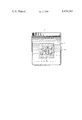
- the FIGURE shows an electroless plating apparatus useful in the practice of the invention.
- the invention in broad terms involves the discovery that for electroless plating of palladium, an acid solution of palladium in the presence of certain organic ligands and with a narrow class of reducing agents yields excellent results both in terms of the plating speed and quality and in terms of the stability and shelf-life of the plating solution.
- the reducing agent should be one or more of the substances selected from the following: formaldehyde, formic acid, hypophosphoric acid and trimethoxyborohydride. Formaldehyde is preferred because of availability and the excellent results obtained.
- Some reducing agents may be added as salts (sodium or potassium formate, sodium or potassium hypophosphate, etc.) but are converted to the acid form in the acidic plating solution.
- the plating solution contains a source of palladium, usually added as a palladium salt such as palladium chloride, palladium bromide, palladium nitrate, palladium sulfate, palladium oxide or hydroxide.
- concentration in terms of palladium metal may vary over large limits including from about 0.001 to 1.0 molar but generally relatively low concentrations (0.01 to 0.2 molar) are preferred because the solution is more stable and large amounts of palladium are not needlessly kept in the solution.
- the electroless plating solution is aqueous and acidic, preferable with pH less than two. More preferably, pH should be less than 1.5 or even 1.0.
- the solution is made acidic by the addition of an acid agent such as nitric acid, hydrochloric acid, sulfuric acid, etc.
- Typical additives are organic ligands selected from a particular class of organic acids. Suitable organic ligands are monocarboxylic acids with up to 10 carbon atoms and dicarboxylic acids with up to 10 carbon atoms. Also useful are sulfonic acids with up to 10 carbon atoms, sulfanilic acid (4-aminobenzenesulfonic acid) and sulfamic acid.
- the carboxylic acid and dicarboxylic acids may have certain substituents in the carbon chain, namely chlorine, bromine and hydroxyl groups.
- the sulfonic acid may have in addition to chlorine, bromine and hydroxyl substitution, aromatic substitutions such as benzene (C 6 H 5 --), chlorobenzene, bromobenzene and hydroxybenzene.
- aromatic substitutions such as benzene (C 6 H 5 --), chlorobenzene, bromobenzene and hydroxybenzene.
- organic ligands tend to stabilize the electroless plating solution possibly by complexing with the palladium ion.
- the presence of the organic ligand in the plating solution greatly improves the quality of the plating with regard to smoothness, brightness, uniformity and adherence.
- the exact mechanism for this behavior is not known, one possibility is that the organic ligand coats the surface to be plated.
- Other organic ligands may also be useful including organic amines, etc. Concentrations may vary over large limits, including from 0.001 molar to about 1.0 molar. Generally, 0.1 to 0.5 molar yields excellent results.
- the reducing agent is crucial to the proper operation of the process.
- the reducing agent should be strong enough to insure proper reduction of the palladium without being so strong as to induce spontaneous reduction in the absence of the surface to be plated.
- reducing agents namely formaldehyde, formic acid, hypophosphoric acid and trimethoxyborohydride in aqueous medium are suitable as reducing agents for the electroless plating of palladium in acid medium.
- formaldehyde both from the point of view of availability, low cost, etc., and because of solution stability and the excellent plating results obtained.
- Concentrations of the reducing agent may vary over large limits, including from about 0.001 to 2.0 molar. Best results are obtained from 0.01 to 1.0 molar. Too low a concentration slows the deposition rate and requires too frequent replenishment of reducing agent; too high a concentration increases the danger of spontaneous deposition.
- the reducing agent is replenished so as to keep its concentration range within the limits set forth above. Either bulk replenishment or continuous replenishment is useful in the practice of the invention.
- Certain other additives may optionally be added to the electroless plating solution to improve the appearance and properties of the plated palladium.
- Typical additives are saccharin, cumarin and phenolphthalein. Typical concentrations are 0.001 to 0.1 molar with 0.001 to 0.01 molar preferred. Below 0.001, no effect is likely and above 0.1 molar no additional benefits are found and it might limit the solubility of other components of the bath.
- a solution is made up of 0.1 molar palladium chloride, 0.4 molar formic acid, 1.0 molar nitric acid, 2.0 molar formaldehyde (added as an aqueous solution) and a small amount (about 0.002 molar) of saccharin.
- the plating is carried out on coupons of brass previously cleaned by first exposing the surface to 20 percent aqueous sulfuric acid, rinsing with deionized water, ultrasonically cleaning in an alkaline cleaner, again cleaning in 20 percent aqueous sulfuric acid and finally rinsing in deionized water.
- Plating is carried out by exposing the surface of the coupons to the plating solution for a measured amount of time, generally 5 minutes.
- the plating solution is mildly agitated during plating.
- the deposits are bright and adherent. Excellent results are also obtained on copper and gold substrates.
- the plated coupons are sectioned to obtain thickness measurements.
- the plating rate is about 6 microinches per minute.
- Plating is also obtained on semiconductor surfaces such as gallium arsenide, indium phosphide and silicon.
- the gallium arsenide and indium phosphide is cleaned with a one percent bromine in methanol solution.
- the silicon surface is cleaned using an HF-peroxide solution.
- the procedure can be used to electrolessly plate palladium on non-catalytic surfaces by activating these surfaces by well-known procedures.
- an activation solution may be used on the surface covered with catalytic metal by evaporation or other means.
- initial deposition might occur by chemical deposition or replacement plating (e.g., where palladium ions in the electroless plating solution reacts with a metal on the surface being plated) and the thin layer of palladium so deposited acts as the catalytic metal for the autocatalytic electroless process described above.
- the FIGURE shows an exemplatory plating apparatus 10 useful in the practice of the invention including vessel 11 to contain the plating solution 12, plastic board 13 with strips 14 of catalytic material to be plated electrolessly with palladium.
Abstract
Description
Claims (13)
Priority Applications (1)
| Application Number | Priority Date | Filing Date | Title |
|---|---|---|---|
| US06/424,150 US4424241A (en) | 1982-09-27 | 1982-09-27 | Electroless palladium process |
Applications Claiming Priority (1)
| Application Number | Priority Date | Filing Date | Title |
|---|---|---|---|
| US06/424,150 US4424241A (en) | 1982-09-27 | 1982-09-27 | Electroless palladium process |
Publications (1)
| Publication Number | Publication Date |
|---|---|
| US4424241A true US4424241A (en) | 1984-01-03 |
Family
ID=23681649
Family Applications (1)
| Application Number | Title | Priority Date | Filing Date |
|---|---|---|---|
| US06/424,150 Expired - Lifetime US4424241A (en) | 1982-09-27 | 1982-09-27 | Electroless palladium process |
Country Status (1)
| Country | Link |
|---|---|
| US (1) | US4424241A (en) |
Cited By (45)
| Publication number | Priority date | Publication date | Assignee | Title |
|---|---|---|---|---|
| US5206055A (en) * | 1991-09-03 | 1993-04-27 | General Electric Company | Method for enhancing the uniform electroless deposition of gold onto a palladium substrate |
| US5264288A (en) * | 1992-10-01 | 1993-11-23 | Ppg Industries, Inc. | Electroless process using silylated polyamine-noble metal complexes |
| US5380560A (en) * | 1992-07-28 | 1995-01-10 | International Business Machines Corporation | Palladium sulfate solution for the selective seeding of the metal interconnections on polyimide dielectrics for electroless metal deposition |
| US5384154A (en) * | 1991-06-12 | 1995-01-24 | U.S. Philips Corporation | Method of selectively providing a pattern of a material other than glass on a glass substrate by electroless metallization |
| EP0692554A1 (en) * | 1994-07-14 | 1996-01-17 | Matsushita Electric Industrial Co., Ltd. | Electroless plating bath used for forming a wiring of a semiconductor device, and method of forming a wiring of a semiconductor device |
| EP0697805A1 (en) | 1994-08-05 | 1996-02-21 | LeaRonal, Inc. | Printed circuit board manufacture utilizing electroless palladium |
| WO1996011751A1 (en) * | 1994-10-17 | 1996-04-25 | Rd Chemical Company | Noble metal coating method by immersion |
| GB2295624A (en) * | 1994-12-02 | 1996-06-05 | Motorola Inc | Method and reduction solution for metallizing a surface |
| DE19631565A1 (en) * | 1996-07-24 | 1998-01-29 | Atotech Deutschland Gmbh | Uniform adherent palladium contact bump production |
| US5882736A (en) * | 1993-05-13 | 1999-03-16 | Atotech Deutschland Gmbh | palladium layers deposition process |
| WO2000059635A1 (en) * | 1999-04-07 | 2000-10-12 | Basf Aktiengesellschaft | Method for producing platinum metal catalysts |
| US6156413A (en) * | 1996-10-25 | 2000-12-05 | Canon Kabushiki Kaisha | Glass circuit substrate and fabrication method thereof |
| US6291025B1 (en) * | 1999-06-04 | 2001-09-18 | Argonide Corporation | Electroless coatings formed from organic liquids |
| DE10018025A1 (en) * | 2000-04-04 | 2001-10-18 | Atotech Deutschland Gmbh | Production of solderable surface on circuit carriers in circuit board manufacture comprises preparing a dielectric substrate having copper structures, producing solderable surfaces, and forming functional surfaces in functional regions |
| US20030130148A1 (en) * | 2001-12-12 | 2003-07-10 | Lee Geun Su | Cleaning solution for removing photoresist |
| US20030207206A1 (en) * | 2002-04-22 | 2003-11-06 | General Electric Company | Limited play data storage media and method for limiting access to data thereon |
| US6779711B2 (en) * | 1999-05-14 | 2004-08-24 | International Business Machines Corporation | Self-aligned corrosion stop for copper C4 and wirebond |
| US20050085031A1 (en) * | 2003-10-15 | 2005-04-21 | Applied Materials, Inc. | Heterogeneous activation layers formed by ionic and electroless reactions used for IC interconnect capping layers |
| US20050095830A1 (en) * | 2003-10-17 | 2005-05-05 | Applied Materials, Inc. | Selective self-initiating electroless capping of copper with cobalt-containing alloys |
| US20050101130A1 (en) * | 2003-11-07 | 2005-05-12 | Applied Materials, Inc. | Method and tool of chemical doping CoW alloys with Re for increasing barrier properties of electroless capping layers for IC Cu interconnects |
| US20050161338A1 (en) * | 2004-01-26 | 2005-07-28 | Applied Materials, Inc. | Electroless cobalt alloy deposition process |
| US20050170650A1 (en) * | 2004-01-26 | 2005-08-04 | Hongbin Fang | Electroless palladium nitrate activation prior to cobalt-alloy deposition |
| WO2006005605A1 (en) * | 2004-07-14 | 2006-01-19 | Dr.-Ing. Max Schlötter Gmbh & Co. Kg | Method for improving solderability of nickel coatings |
| US20060246699A1 (en) * | 2005-03-18 | 2006-11-02 | Weidman Timothy W | Process for electroless copper deposition on a ruthenium seed |
| US20060251800A1 (en) * | 2005-03-18 | 2006-11-09 | Weidman Timothy W | Contact metallization scheme using a barrier layer over a silicide layer |
| US20060264043A1 (en) * | 2005-03-18 | 2006-11-23 | Stewart Michael P | Electroless deposition process on a silicon contact |
| US20070071888A1 (en) * | 2005-09-21 | 2007-03-29 | Arulkumar Shanmugasundram | Method and apparatus for forming device features in an integrated electroless deposition system |
| US20070108404A1 (en) * | 2005-10-28 | 2007-05-17 | Stewart Michael P | Method of selectively depositing a thin film material at a semiconductor interface |
| US20080138528A1 (en) * | 2005-01-12 | 2008-06-12 | Umicore Galvanotechnik Gmbh | Method for Depositing Palladium Layers and Palladium Bath Therefor |
| US20090044720A1 (en) * | 2007-08-15 | 2009-02-19 | Kojima Chemicals Co., Ltd. | Electroless palladium plating solution |
| US20090133603A1 (en) * | 2005-09-27 | 2009-05-28 | C. Uyemura & Co., Ltd | Electroless palladium plating bath and electroless palladium plating method |
| US7651934B2 (en) | 2005-03-18 | 2010-01-26 | Applied Materials, Inc. | Process for electroless copper deposition |
| EP2177646A1 (en) | 2008-10-17 | 2010-04-21 | Atotech Deutschland Gmbh | Stress-reduced Ni-P/Pd stacks for bondable wafer surfaces |
| US20100098863A1 (en) * | 2003-03-12 | 2010-04-22 | University Of Missouri | Process for spontaneous deposition from an organic solution |
| US20110065274A1 (en) * | 2009-08-25 | 2011-03-17 | Rohm And Haas Electronic Materials Llc | Enhanced method of forming nickel silicides |
| US20120118196A1 (en) * | 2009-05-08 | 2012-05-17 | Kojima Chemicals Co., Ltd. | Electroless palladium plating solution |
| EP2469992A1 (en) | 2010-12-23 | 2012-06-27 | Atotech Deutschland GmbH | Method for obtaining a palladium surface finish for copper wire bonding on printed circuit boards and IC-substrates |
| EP2535929A1 (en) | 2011-06-14 | 2012-12-19 | Atotech Deutschland GmbH | Wire bondable surface for microelectronic devices |
| EP2887779A1 (en) | 2013-12-20 | 2015-06-24 | ATOTECH Deutschland GmbH | Silver wire bonding on printed circuit boards and IC-substrates |
| WO2015155173A1 (en) * | 2014-04-10 | 2015-10-15 | Atotech Deutschland Gmbh | Plating bath composition and method for electroless plating of palladium |
| WO2016097083A2 (en) | 2014-12-17 | 2016-06-23 | Atotech Deutschland Gmbh | Plating bath composition and method for electroless plating of palladium |
| WO2016097084A1 (en) | 2014-12-17 | 2016-06-23 | Atotech Deutschland Gmbh | Plating bath composition and method for electroless plating of palladium |
| WO2018036951A1 (en) | 2016-08-23 | 2018-03-01 | Atotech Deutschland Gmbh | Method for directly depositing palladium onto a non-activated surface of a gallium nitride semiconductor |
| WO2022043567A1 (en) | 2020-08-31 | 2022-03-03 | Atotech Deutschland GmbH & Co. KG | Compostion for depositing a palladium coating on a substrate |
| EP4215642A1 (en) | 2022-01-25 | 2023-07-26 | Atotech Deutschland GmbH & Co. KG | Compostion for depositing a palladium coating on an activated copper-coated substrate |
-
1982
- 1982-09-27 US US06/424,150 patent/US4424241A/en not_active Expired - Lifetime
Non-Patent Citations (1)
| Title |
|---|
| Coleman et al., "The Pd2 Si-(PD)-Ni Solder Plated Metallization . . . " Conference: 13th IEEE Photovoltaic Specialists Conference-1978, Washington, DC USA (Jun. 5-8 1978). |
Cited By (78)
| Publication number | Priority date | Publication date | Assignee | Title |
|---|---|---|---|---|
| US5384154A (en) * | 1991-06-12 | 1995-01-24 | U.S. Philips Corporation | Method of selectively providing a pattern of a material other than glass on a glass substrate by electroless metallization |
| US5206055A (en) * | 1991-09-03 | 1993-04-27 | General Electric Company | Method for enhancing the uniform electroless deposition of gold onto a palladium substrate |
| US5380560A (en) * | 1992-07-28 | 1995-01-10 | International Business Machines Corporation | Palladium sulfate solution for the selective seeding of the metal interconnections on polyimide dielectrics for electroless metal deposition |
| US5264288A (en) * | 1992-10-01 | 1993-11-23 | Ppg Industries, Inc. | Electroless process using silylated polyamine-noble metal complexes |
| US5882736A (en) * | 1993-05-13 | 1999-03-16 | Atotech Deutschland Gmbh | palladium layers deposition process |
| US5645628A (en) * | 1994-07-14 | 1997-07-08 | Matsushita Electric Industrial Co., Ltd. | Electroless plating bath used for forming a wiring of a semiconductor device, and method of forming a wiring of a semiconductor device |
| EP0692554A1 (en) * | 1994-07-14 | 1996-01-17 | Matsushita Electric Industrial Co., Ltd. | Electroless plating bath used for forming a wiring of a semiconductor device, and method of forming a wiring of a semiconductor device |
| EP0697805A1 (en) | 1994-08-05 | 1996-02-21 | LeaRonal, Inc. | Printed circuit board manufacture utilizing electroless palladium |
| WO1996011751A1 (en) * | 1994-10-17 | 1996-04-25 | Rd Chemical Company | Noble metal coating method by immersion |
| GB2295624B (en) * | 1994-12-02 | 1998-07-29 | Motorola Inc | Method for metallizing a surface |
| GB2295624A (en) * | 1994-12-02 | 1996-06-05 | Motorola Inc | Method and reduction solution for metallizing a surface |
| DE19631565A1 (en) * | 1996-07-24 | 1998-01-29 | Atotech Deutschland Gmbh | Uniform adherent palladium contact bump production |
| US6156413A (en) * | 1996-10-25 | 2000-12-05 | Canon Kabushiki Kaisha | Glass circuit substrate and fabrication method thereof |
| WO2000059635A1 (en) * | 1999-04-07 | 2000-10-12 | Basf Aktiengesellschaft | Method for producing platinum metal catalysts |
| US6676919B1 (en) | 1999-04-07 | 2004-01-13 | Basf Aktiengesellschaft | Method for producing platinum metal catalysts |
| US6779711B2 (en) * | 1999-05-14 | 2004-08-24 | International Business Machines Corporation | Self-aligned corrosion stop for copper C4 and wirebond |
| US7081680B2 (en) * | 1999-05-14 | 2006-07-25 | International Business Machines - Corporation | Self-aligned corrosion stop for copper C4 and wirebond |
| US20040234679A1 (en) * | 1999-05-14 | 2004-11-25 | Edelstein Daniel C. | Self-aligned corrosion stop for copper C4 and wirebond |
| US6291025B1 (en) * | 1999-06-04 | 2001-09-18 | Argonide Corporation | Electroless coatings formed from organic liquids |
| DE10018025A1 (en) * | 2000-04-04 | 2001-10-18 | Atotech Deutschland Gmbh | Production of solderable surface on circuit carriers in circuit board manufacture comprises preparing a dielectric substrate having copper structures, producing solderable surfaces, and forming functional surfaces in functional regions |
| US6698648B2 (en) | 2000-04-04 | 2004-03-02 | Atotech Deutschland Gmbh | Method for producing solderable and functional surfaces on circuit carriers |
| US20030130148A1 (en) * | 2001-12-12 | 2003-07-10 | Lee Geun Su | Cleaning solution for removing photoresist |
| US7563753B2 (en) * | 2001-12-12 | 2009-07-21 | Hynix Semiconductor Inc. | Cleaning solution for removing photoresist |
| US20030207206A1 (en) * | 2002-04-22 | 2003-11-06 | General Electric Company | Limited play data storage media and method for limiting access to data thereon |
| US20100098863A1 (en) * | 2003-03-12 | 2010-04-22 | University Of Missouri | Process for spontaneous deposition from an organic solution |
| US20050085031A1 (en) * | 2003-10-15 | 2005-04-21 | Applied Materials, Inc. | Heterogeneous activation layers formed by ionic and electroless reactions used for IC interconnect capping layers |
| US20050095830A1 (en) * | 2003-10-17 | 2005-05-05 | Applied Materials, Inc. | Selective self-initiating electroless capping of copper with cobalt-containing alloys |
| US20050101130A1 (en) * | 2003-11-07 | 2005-05-12 | Applied Materials, Inc. | Method and tool of chemical doping CoW alloys with Re for increasing barrier properties of electroless capping layers for IC Cu interconnects |
| US7205233B2 (en) | 2003-11-07 | 2007-04-17 | Applied Materials, Inc. | Method for forming CoWRe alloys by electroless deposition |
| US20050161338A1 (en) * | 2004-01-26 | 2005-07-28 | Applied Materials, Inc. | Electroless cobalt alloy deposition process |
| US20050170650A1 (en) * | 2004-01-26 | 2005-08-04 | Hongbin Fang | Electroless palladium nitrate activation prior to cobalt-alloy deposition |
| WO2006005605A1 (en) * | 2004-07-14 | 2006-01-19 | Dr.-Ing. Max Schlötter Gmbh & Co. Kg | Method for improving solderability of nickel coatings |
| US20080138528A1 (en) * | 2005-01-12 | 2008-06-12 | Umicore Galvanotechnik Gmbh | Method for Depositing Palladium Layers and Palladium Bath Therefor |
| US8308858B2 (en) | 2005-03-18 | 2012-11-13 | Applied Materials, Inc. | Electroless deposition process on a silicon contact |
| US20060264043A1 (en) * | 2005-03-18 | 2006-11-23 | Stewart Michael P | Electroless deposition process on a silicon contact |
| US20060252252A1 (en) * | 2005-03-18 | 2006-11-09 | Zhize Zhu | Electroless deposition processes and compositions for forming interconnects |
| US20100107927A1 (en) * | 2005-03-18 | 2010-05-06 | Stewart Michael P | Electroless deposition process on a silicon contact |
| US20060251800A1 (en) * | 2005-03-18 | 2006-11-09 | Weidman Timothy W | Contact metallization scheme using a barrier layer over a silicide layer |
| US20060246699A1 (en) * | 2005-03-18 | 2006-11-02 | Weidman Timothy W | Process for electroless copper deposition on a ruthenium seed |
| US7659203B2 (en) | 2005-03-18 | 2010-02-09 | Applied Materials, Inc. | Electroless deposition process on a silicon contact |
| US7651934B2 (en) | 2005-03-18 | 2010-01-26 | Applied Materials, Inc. | Process for electroless copper deposition |
| US20070071888A1 (en) * | 2005-09-21 | 2007-03-29 | Arulkumar Shanmugasundram | Method and apparatus for forming device features in an integrated electroless deposition system |
| US20090133603A1 (en) * | 2005-09-27 | 2009-05-28 | C. Uyemura & Co., Ltd | Electroless palladium plating bath and electroless palladium plating method |
| US7678183B2 (en) * | 2005-09-27 | 2010-03-16 | C. Uyemura & Co., Ltd. | Electroless palladium plating bath and electroless palladium plating method |
| US20070108404A1 (en) * | 2005-10-28 | 2007-05-17 | Stewart Michael P | Method of selectively depositing a thin film material at a semiconductor interface |
| US7632343B2 (en) * | 2007-08-15 | 2009-12-15 | Kojima Chemicals Co., Ltd. | Electroless palladium plating solution |
| US20090044720A1 (en) * | 2007-08-15 | 2009-02-19 | Kojima Chemicals Co., Ltd. | Electroless palladium plating solution |
| EP2177646A1 (en) | 2008-10-17 | 2010-04-21 | Atotech Deutschland Gmbh | Stress-reduced Ni-P/Pd stacks for bondable wafer surfaces |
| WO2010043502A1 (en) * | 2008-10-17 | 2010-04-22 | Atotech Deutschland Gmbh | Stress-reduced ni-p/pd stacks for bondable wafer surfaces |
| KR101610780B1 (en) | 2008-10-17 | 2016-04-08 | 아토테크더치랜드게엠베하 | Stress-Reduced Ni-P/Pd Stacks for Bondable Wafer Surfaces |
| US8986789B2 (en) | 2008-10-17 | 2015-03-24 | Atotech Deutschland Gmbh | Stress-reduced Ni-P/Pd stacks for bondable wafer surfaces |
| US20110200842A1 (en) * | 2008-10-17 | 2011-08-18 | Atotech Deutschland Gmbh | Stress-reduced ni-p/pd stacks for bondable wafer surfaces |
| CN102482779A (en) * | 2008-10-17 | 2012-05-30 | 安美特德国有限公司 | Stress-reduced ni-p/pd stacks for bondable wafer surfaces |
| CN102482779B (en) * | 2008-10-17 | 2014-06-18 | 安美特德国有限公司 | Stress-reduced ni-p/pd stacks for bondable wafer surfaces |
| US20120118196A1 (en) * | 2009-05-08 | 2012-05-17 | Kojima Chemicals Co., Ltd. | Electroless palladium plating solution |
| US8562727B2 (en) * | 2009-05-08 | 2013-10-22 | Kojima Chemicals Co., Ltd. | Electroless palladium plating solution |
| US7955978B2 (en) | 2009-08-25 | 2011-06-07 | Rohm and Hass Electronic Materials LLC | Enhanced method of forming nickel silicides |
| US20110065274A1 (en) * | 2009-08-25 | 2011-03-17 | Rohm And Haas Electronic Materials Llc | Enhanced method of forming nickel silicides |
| EP2469992A1 (en) | 2010-12-23 | 2012-06-27 | Atotech Deutschland GmbH | Method for obtaining a palladium surface finish for copper wire bonding on printed circuit boards and IC-substrates |
| WO2012084736A1 (en) | 2010-12-23 | 2012-06-28 | Atotech Deutschland Gmbh | Method for obtaining a palladium surface finish for copper wire bonding on printed circuit boards and ic-substrates |
| EP2535929A1 (en) | 2011-06-14 | 2012-12-19 | Atotech Deutschland GmbH | Wire bondable surface for microelectronic devices |
| WO2012171727A1 (en) | 2011-06-14 | 2012-12-20 | Atotech Deutschland Gmbh | Wire bondable surface for microelectronic devices |
| EP2887779A1 (en) | 2013-12-20 | 2015-06-24 | ATOTECH Deutschland GmbH | Silver wire bonding on printed circuit boards and IC-substrates |
| US9758874B2 (en) | 2014-04-10 | 2017-09-12 | Atotech Deutschland Gmbh | Plating bath composition and method for electroless plating of palladium |
| WO2015155173A1 (en) * | 2014-04-10 | 2015-10-15 | Atotech Deutschland Gmbh | Plating bath composition and method for electroless plating of palladium |
| CN106460182B (en) * | 2014-04-10 | 2019-07-09 | 安美特德国有限公司 | The method of bath compositions and the electroless for palladium |
| CN106460182A (en) * | 2014-04-10 | 2017-02-22 | 安美特德国有限公司 | Plating bath composition and method for electroless plating of palladium |
| WO2016097084A1 (en) | 2014-12-17 | 2016-06-23 | Atotech Deutschland Gmbh | Plating bath composition and method for electroless plating of palladium |
| CN107109653A (en) * | 2014-12-17 | 2017-08-29 | 埃托特克德国有限公司 | Bath compositions and method for chemical palladium-plating |
| JP2017538867A (en) * | 2014-12-17 | 2017-12-28 | アトテツク・ドイチユラント・ゲゼルシヤフト・ミツト・ベシユレンクテル・ハフツングAtotech Deutschland GmbH | Plating bath composition for electroless plating of palladium and electroless plating method of palladium |
| WO2016097083A2 (en) | 2014-12-17 | 2016-06-23 | Atotech Deutschland Gmbh | Plating bath composition and method for electroless plating of palladium |
| US10385458B2 (en) | 2014-12-17 | 2019-08-20 | Atotech Deutschland Gmbh | Plating bath composition and method for electroless plating of palladium |
| TWI680207B (en) * | 2014-12-17 | 2019-12-21 | 德商德國艾托特克公司 | Plating bath composition and method for electroless plating of palladium |
| WO2018036951A1 (en) | 2016-08-23 | 2018-03-01 | Atotech Deutschland Gmbh | Method for directly depositing palladium onto a non-activated surface of a gallium nitride semiconductor |
| US10920322B2 (en) | 2016-08-23 | 2021-02-16 | Atotech Deutschland Gmbh | Method for directly depositing palladium onto a non-activated surface of a gallium nitride semiconductor |
| WO2022043567A1 (en) | 2020-08-31 | 2022-03-03 | Atotech Deutschland GmbH & Co. KG | Compostion for depositing a palladium coating on a substrate |
| EP4215642A1 (en) | 2022-01-25 | 2023-07-26 | Atotech Deutschland GmbH & Co. KG | Compostion for depositing a palladium coating on an activated copper-coated substrate |
| WO2023144003A1 (en) | 2022-01-25 | 2023-08-03 | Atotech Deutschland GmbH & Co. KG | Composition for depositing a palladium coating on an activated copper-coated substrate |
Similar Documents
| Publication | Publication Date | Title |
|---|---|---|
| US4424241A (en) | Electroless palladium process | |
| US3993491A (en) | Electroless plating | |
| US4021314A (en) | Method of depositing a metal on a surface | |
| US3075856A (en) | Copper plating process and solution | |
| EP0503389B1 (en) | Process for electroless plating tin, lead or tin-lead alloy | |
| US3011920A (en) | Method of electroless deposition on a substrate and catalyst solution therefor | |
| US3269861A (en) | Method for electroless copper plating | |
| US4919768A (en) | Electroplating process | |
| US4301196A (en) | Electroless copper deposition process having faster plating rates | |
| JP3314966B2 (en) | Complexing agent for displacement tin plating | |
| US4600609A (en) | Method and composition for electroless nickel deposition | |
| US3672923A (en) | Solid precious metal sensitizing compositions | |
| US3627558A (en) | Sensitization process for electroless plating | |
| US6855191B2 (en) | Electroless gold plating solution | |
| JPH04232278A (en) | Conditioning of substrate for electroless plating onto substrate | |
| EP0216531A1 (en) | Use of immersion tin and tin alloys as a bonding medium for multilayer circuits | |
| US3075855A (en) | Copper plating process and solutions | |
| US4150171A (en) | Electroless plating | |
| US3993848A (en) | Catalytic primer | |
| KR20150136066A (en) | Electroless copper plating solution | |
| US4816070A (en) | Use of immersion tin and alloys as a bonding medium for multilayer circuits | |
| JP3337802B2 (en) | Direct plating method by metallization of copper (I) oxide colloid | |
| JPS5925965A (en) | Non-electrolytic copper deposition having rapid plating speed | |
| US3666527A (en) | Method of electroless deposition of metals with improved sensitizer | |
| US6875474B2 (en) | Electroless copper plating solutions and methods of use thereof |
Legal Events
| Date | Code | Title | Description |
|---|---|---|---|
| AS | Assignment |
Owner name: BELL TELEPHONE LABORATORIES, INCORPORATED; 600 MOU Free format text: ASSIGNMENT OF ASSIGNORS INTEREST.;ASSIGNOR:ABYS, JOSEPH A.;REEL/FRAME:004093/0556 Effective date: 19820922 |
|
| STCF | Information on status: patent grant |
Free format text: PATENTED CASE |
|
| MAFP | Maintenance fee payment |
Free format text: PAYMENT OF MAINTENANCE FEE, 4TH YEAR, PL 97-247 (ORIGINAL EVENT CODE: M173); ENTITY STATUS OF PATENT OWNER: LARGE ENTITY Year of fee payment: 4 |
|
| FEPP | Fee payment procedure |
Free format text: PAYOR NUMBER ASSIGNED (ORIGINAL EVENT CODE: ASPN); ENTITY STATUS OF PATENT OWNER: LARGE ENTITY |
|
| MAFP | Maintenance fee payment |
Free format text: PAYMENT OF MAINTENANCE FEE, 8TH YEAR, PL 97-247 (ORIGINAL EVENT CODE: M174); ENTITY STATUS OF PATENT OWNER: LARGE ENTITY Year of fee payment: 8 |
|
| MAFP | Maintenance fee payment |
Free format text: PAYMENT OF MAINTENANCE FEE, 12TH YEAR, LARGE ENTITY (ORIGINAL EVENT CODE: M185); ENTITY STATUS OF PATENT OWNER: LARGE ENTITY Year of fee payment: 12 |