EP0689099A1 - Apparat zur Projektionsbelichtung und Verfahren zur Herstellung einer Vorrichtung unter Verwendung desselben - Google Patents
Apparat zur Projektionsbelichtung und Verfahren zur Herstellung einer Vorrichtung unter Verwendung desselben Download PDFInfo
- Publication number
- EP0689099A1 EP0689099A1 EP95304381A EP95304381A EP0689099A1 EP 0689099 A1 EP0689099 A1 EP 0689099A1 EP 95304381 A EP95304381 A EP 95304381A EP 95304381 A EP95304381 A EP 95304381A EP 0689099 A1 EP0689099 A1 EP 0689099A1
- Authority
- EP
- European Patent Office
- Prior art keywords
- light
- optical system
- projection
- projection optical
- reticle
- Prior art date
- Legal status (The legal status is an assumption and is not a legal conclusion. Google has not performed a legal analysis and makes no representation as to the accuracy of the status listed.)
- Granted
Links
Images


Classifications
-
- H—ELECTRICITY
- H01—ELECTRIC ELEMENTS
- H01L—SEMICONDUCTOR DEVICES NOT COVERED BY CLASS H10
- H01L21/00—Processes or apparatus adapted for the manufacture or treatment of semiconductor or solid state devices or of parts thereof
- H01L21/02—Manufacture or treatment of semiconductor devices or of parts thereof
- H01L21/027—Making masks on semiconductor bodies for further photolithographic processing not provided for in group H01L21/18 or H01L21/34
-
- G—PHYSICS
- G03—PHOTOGRAPHY; CINEMATOGRAPHY; ANALOGOUS TECHNIQUES USING WAVES OTHER THAN OPTICAL WAVES; ELECTROGRAPHY; HOLOGRAPHY
- G03F—PHOTOMECHANICAL PRODUCTION OF TEXTURED OR PATTERNED SURFACES, e.g. FOR PRINTING, FOR PROCESSING OF SEMICONDUCTOR DEVICES; MATERIALS THEREFOR; ORIGINALS THEREFOR; APPARATUS SPECIALLY ADAPTED THEREFOR
- G03F7/00—Photomechanical, e.g. photolithographic, production of textured or patterned surfaces, e.g. printing surfaces; Materials therefor, e.g. comprising photoresists; Apparatus specially adapted therefor
- G03F7/70—Microphotolithographic exposure; Apparatus therefor
- G03F7/70483—Information management; Active and passive control; Testing; Wafer monitoring, e.g. pattern monitoring
- G03F7/7055—Exposure light control in all parts of the microlithographic apparatus, e.g. pulse length control or light interruption
- G03F7/70558—Dose control, i.e. achievement of a desired dose
-
- G—PHYSICS
- G03—PHOTOGRAPHY; CINEMATOGRAPHY; ANALOGOUS TECHNIQUES USING WAVES OTHER THAN OPTICAL WAVES; ELECTROGRAPHY; HOLOGRAPHY
- G03F—PHOTOMECHANICAL PRODUCTION OF TEXTURED OR PATTERNED SURFACES, e.g. FOR PRINTING, FOR PROCESSING OF SEMICONDUCTOR DEVICES; MATERIALS THEREFOR; ORIGINALS THEREFOR; APPARATUS SPECIALLY ADAPTED THEREFOR
- G03F7/00—Photomechanical, e.g. photolithographic, production of textured or patterned surfaces, e.g. printing surfaces; Materials therefor, e.g. comprising photoresists; Apparatus specially adapted therefor
- G03F7/70—Microphotolithographic exposure; Apparatus therefor
- G03F7/70058—Mask illumination systems
- G03F7/70133—Measurement of illumination distribution, in pupil plane or field plane
-
- G—PHYSICS
- G03—PHOTOGRAPHY; CINEMATOGRAPHY; ANALOGOUS TECHNIQUES USING WAVES OTHER THAN OPTICAL WAVES; ELECTROGRAPHY; HOLOGRAPHY
- G03F—PHOTOMECHANICAL PRODUCTION OF TEXTURED OR PATTERNED SURFACES, e.g. FOR PRINTING, FOR PROCESSING OF SEMICONDUCTOR DEVICES; MATERIALS THEREFOR; ORIGINALS THEREFOR; APPARATUS SPECIALLY ADAPTED THEREFOR
- G03F7/00—Photomechanical, e.g. photolithographic, production of textured or patterned surfaces, e.g. printing surfaces; Materials therefor, e.g. comprising photoresists; Apparatus specially adapted therefor
- G03F7/70—Microphotolithographic exposure; Apparatus therefor
- G03F7/70216—Mask projection systems
- G03F7/70241—Optical aspects of refractive lens systems, i.e. comprising only refractive elements
-
- G—PHYSICS
- G03—PHOTOGRAPHY; CINEMATOGRAPHY; ANALOGOUS TECHNIQUES USING WAVES OTHER THAN OPTICAL WAVES; ELECTROGRAPHY; HOLOGRAPHY
- G03F—PHOTOMECHANICAL PRODUCTION OF TEXTURED OR PATTERNED SURFACES, e.g. FOR PRINTING, FOR PROCESSING OF SEMICONDUCTOR DEVICES; MATERIALS THEREFOR; ORIGINALS THEREFOR; APPARATUS SPECIALLY ADAPTED THEREFOR
- G03F7/00—Photomechanical, e.g. photolithographic, production of textured or patterned surfaces, e.g. printing surfaces; Materials therefor, e.g. comprising photoresists; Apparatus specially adapted therefor
- G03F7/70—Microphotolithographic exposure; Apparatus therefor
- G03F7/70483—Information management; Active and passive control; Testing; Wafer monitoring, e.g. pattern monitoring
- G03F7/70591—Testing optical components
- G03F7/706—Aberration measurement
Definitions
- This invention relates to a projection exposure apparatus and a device manufacturing method for manufacturing microdevices such as ICs, LSIs, liquid crystal devices or magnetic heads, for example, by using such a projection exposure apparatus.
- a projection optical system absorbs a portion of exposure light energy so that it is heated. The absorbed heat is then radiated. This causes shift of the position of the imaging plane of the projection optical system or a change of the projection magnification.
- Such shift of the imaging plane or change in the projection magnification may be detected on the basis of equations with parameters such as total light quantity passing a reticle pattern, the time consumed for the exposure process and the time between successive exposures in addition to the time constant peculiar to the projection optical system. Then, drive of a wafer stage or drive of a lens or lenses of the projection optical system or the pressure between lenses of the projection optical system may be controlled to correct the shift of the imaging plane or the change of the projection magnification.
- a projection exposure apparatus comprising: a projection optical system for projecting a pattern of a reticle onto a substrate; optical characteristic detecting means for detecting a change in optical characteristic of said projection optical system, which change may results from the projection of the reticle pattern onto the substrate through said projection optical system; and light detecting means for detecting at least one of (i) an intensity distribution of light from the reticle pattern, at a position adjacent to the reticle or adjacent to an imaging plane on which the reticle is to be imaged, and (ii) an intensity distribution of the light from the reticle pattern, at a position adjacent to a pupil plane of said projection optical system; wherein said optical characteristic detecting means is arranged to detect the amount of change in optical characteristic in accordance with the intensity distribution detected by said light detecting means.
- a projection exposure apparatus comprising: a projection optical system for projecting a pattern of a reticle onto a substrate; optical characteristic detecting means for detecting a change in optical characteristic of said projection optical system, which change may results from the projection of the reticle pattern onto the substrate through said projection optical system; optical characteristic correcting means for substantially correcting the change in optical characteristic of said projection optical system in accordance with an output of said optical characteristic detecting means; and light detecting means for detecting at least one of (i) an intensity distribution of light from the reticle pattern, at a position adjacent to the reticle or adjacent to an imaging plane on which the reticle is to be imaged, and (ii) an intensity distribution of the light from the reticle pattern, at a position adjacent to a pupil plane of said projection optical system; wherein said optical characteristic detecting means is arranged to detect the amount of change in optical characteristic in accordance with the intensity distribution detected by said light detecting means.
- said optical characteristic detecting means is arranged to detect at least one of the amount of change of said imaging plane of said projection optical system and the amount of change of projection magnification.
- said optical characteristic correcting means is arranged to correct at least one of the amount of change in said imaging plane of said projection optical system and the amount of change in projection magnification.
- said optical characteristic detecting means and said optical characteristic correcting means are arranged to detect and correct the change of said imaging plane of said projection optical system and the change of projection magnification thereof.
- said light detecting means includes first light detector means having a light detecting surface adjacent to said imaging plane of said projection optical system, for detecting a light intensity distribution adjacent to the reticle, and second light detector means having a light detecting surface at a position away from said imaging plane of said projection optical system, for detecting a light intensity distribution adjacent to the pupil plane of said projection optical system.
- said light detecting means includes a light blocking plate with a pinhole disposed adjacent to said imaging plane, and a plurality of photoelectric converting elements arrayed at a position away from said imaging plane for detecting light passing through the reticle pattern and through said projection optical system and coming from said light blocking plate, wherein the light intensity distribution adjacent to the pupil plane of said projection optical system is determined on the basis of an output distribution of said photoelectric converting elements, wherein the light intensity adjacent to the reticle is determined on the basis of the sum of outputs of said photoelectric converting elements, and wherein said light blocking plate and said photoelectric converting elements are movable as a unit along said imaging plane.
- a projection exposure apparatus such as above is used to print a device pattern of a reticle on a workpiece such as a silicon wafer or a glass substrate, for example, for accurate manufacture of devices such as ICs, LSIs, CCDs, liquid crystal elements or magnetic heads, for example.
- Figure 1 is a schematic view of a projection exposure apparatus according to one embodiment of the present invention.
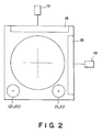
- Figure 2 is a plan view for explaining a modified form of the projection exposure apparatus of Figure 1.
- Figures 3A, 3B and 3C are schematic views for explaining examples of a split sensor.
- Figure 4 is a flow chart of device manufacturing processes.
- Figure 5 is a flow chart of a wafer process in a portion of the flow of Figure 4.
- Figure 1 is a schematic view showing one embodiment of the present invention, wherein the invention is applied to a step-and-repeat type projection exposure apparatus for manufacture of microdevices such as ICs, LSIs, CCDs, liquid crystal elements or magnetic heads, for example.
- microdevices such as ICs, LSIs, CCDs, liquid crystal elements or magnetic heads, for example.
- Denoted in Figure 1 at 1 is an illumination system, and denoted at 2 is a reticle having a device pattern formed thereon.
- Denoted at 3 is a reticle stage, and denoted at 4 is a projection lens system for projecting the device pattern of the reticle 2 in a reduced scale.
- Denoted at 5 is a wafer on which the device pattern of the reticle is to be transferred or printed, and denoted at 6 is a wafer chuck for holding the wafer 5.
- the wafer chuck 6 is movable along the direction of an optical axis 25.
- Denoted at 7 is an X-Y stage for holding the wafer chuck 6.
- the X-Y stage 7 is movable two-dimensionally along a plane perpendicular to the optical axis 25.
- Denoted at 8 is a base on which the projection lens system 4 and the X-Y stage 7, for example, are mounted.
- Denoted at 9 is a stop of the illumination system 1.
- the stop 9 has an opening which is variable in size and in shape.
- Denoted at 10 is a driving mechanism for changing the size or shape of the opening of the stop 9, to thereby change the numerical aperture (N.A.).
- Denoted at 11 is a certain lens of the projection lens system 4, which lens 11 is movable along the optical axis 25 direction.
- Denoted at 12 is a driving mechanism for moving and displacing the lens 11 along the optical axis 25 direction, to thereby change the projection magnification of the projection lens system 4.
- Denoted at 13 is a stop (pupil) of the projection lens system 4.
- the stop 13 is at a position optically conjugate with the stop 9.
- the stop 13 has an opening which is variable in size.
- Denoted at 14 is a driving mechanism for changing the size of the opening of the stop 13, to thereby change the numerical aperture (N.A.).
- Denoted at 15 and 16 are components for detecting the position (level) of the wafer 5 surface with respect to the optical axis 25 direction. More specifically, denoted at 15 is an illumination device for illuminating the wafer 5, and denoted at 16 is a light receiving device for receiving reflected light from the wafer 5 surface and for producing a signal corresponding to the position of the wafer 5 surface. Denoted at 17 is a controller for controlling the components 15 and 16.
- Denoted at 18 is a reflector fixedly mounted on the X-Y stage 7, and denoted at 19 is a laser interferometer for projecting a laser beam to the reflection surface of the reflector 18 and for detecting the amount of displacement of the X-Y stage 7.
- Denoted at 20 is a driving mechanism for controlling movement of the X-Y stage 7 in response to the output of the laser interferometer.
- the driving mechanism 20 receives information related to the level of the wafer 5 surface, from the controller 17. Then, it serves to move the wafer chuck 6 along the optical axis direction, such that the wafer 5 surface is brought into registration with the imaging plane on which the device pattern of the reticle 2 is to be imaged by the projection lens system 4.
- Denoted at 21 is a light blocking plate having a central pinhole
- denoted at 22 is an array of photoelectric converting elements such as CCDs (the array hereinafter will be referred to as "CCD 22").
- the light blocking plate 21 is so set that the surface thereof is at the same level of the wafer 5 surface, and it is disposed adjacent to the imaging plane of the device pattern of the reticle 2 through the projection optical system 4.
- the CCD 22 is disposed at a position which is below and is at a predetermined distance from the light blocking plate 21, so that it receives the light passing through the pinhole of the light blocking plate 21.
- the CCD 22 is at a position spaced away from the imaging plane of the reticle device pattern. This position is such a position about which a light intensity distribution that corresponds to the light intensity distribution of diffraction light from the device pattern of the reticle 2 as produced at the opening of the stop 13 of the projection optical system 4, is produced.
- the light blocking plate 21 and the CCD 22 are fixedly mounted on the X-Y stage 7 as a unit therewith. Thus, by moving the X-ray stage 7, the pinhole of the light blocking plate 21 is positioned sequentially at different positions within the imaging plane and, thus, detection of light intensity or light intensity distribution is enabled at these positions.
- Denoted at 23 is a controller which serves to drive the CCD 22, to receive outputs from the CCD 22, to detect the light intensity distribution of the device pattern image as formed on the imaging plane (which corresponds to the intensity distribution, adjacent to the reticle 2, of the light passed through the device pattern of the reticle 2) and to detect the light intensity distribution at the opening of the stop 13 as formed on the light receiving surface of the CCD 22 (which corresponds to the light intensity distribution at the pupil of the projection optical system 4).
- the light intensity distribution of the device pattern image is detected by moving the X-Y state 7 to sequentially place the pinhole of the light blocking plate 21 at different positions within the imaging plane of the device pattern and by detecting the sum of outputs of the picture elements of the CCD 22 at these positions.
- the light intensity distribution at the opening of the stop 13 is detected by moving the X-Y stage 7 to sequentially place the pinhole of the light blocking plate 21 at different positions within the imaging plane of the device pattern and by detecting an average of the light intensity distributions obtainable from the outputs of the CCD 22 at these positions.
- the controller 23 In addition to the light intensity distribution of the device pattern image, the controller 23 produces, from the outputs of the CCD 22, the information related to the total light quantity of the light passed through the device pattern of the reticle 2.
- Denoted at 24 is a main controller for controlling the elements denoted at 10, 12, 14, 17, 20 and 23.
- Various data such as the information related to the open and closed periods of an exposure controlling shutter (not shown) of the illumination system 1 (that is, the time period t consumed for the exposure and time period t' between successive exposure periods), the information related to the light intensity distribution of the device pattern image from the controller 23, and the information related to the light intensity distribution at the opening of the stop 13 from the controller 23, are all applied to this main controller 24.
- the controller 24 calculates a change ⁇ F of the position of the imaging plane of the device pattern through the projection optical system 4 resulting from the repetition of exposures as well as a change ⁇ of the device pattern projection magnification of the projection lens system 4 also resulting from the repetition of exposures, this being performed in accordance with equations (1) and (2) below. This calculation is done by using equations which are obtainable by modifying conventionally used correction equations by adding parameters dependent upon the light intensity distribution of diffraction light.
- SF and SB are proportional constants;
- QD is a parameter corresponding to the total quantity of light passed through the device pattern;
- Da is a parameter dependent upon the light intensity distribution of the device pattern image (i.e., the distribution of light transmissivity of the device pattern of the reticle 2);
- Db is a parameter dependent upon the light intensity distribution at the opening of the stop 13 (i.e., the light intensity distribution at the pupil plane of the projection optical system 4, of the light from the reticle 2);
- K F and K B are parameters which represent the heat conductivity of the projection lens system 4;
- DT is the ratio of time period, within unit time in calculation, in which period the shutter is kept open;
- ⁇ F' and ⁇ ' are the amount of change of the imaging plane and the amount of change of the magnification, respectively, of the projection lens system as calculated in the preceding unit time just before;
- ⁇ F1 and ⁇ 1 each is the amount of change per unit time of the projection lens system due to heat absorption;
- the changes ⁇ F2 and ⁇ 2 may be expressed in the form of linear coupling of plural terms.
- the values of Da and Db may be determined beforehand, through experiments, for example, in relation to various light intensity distributions to be produced by the controller 23.
- the thus determined data may be stored into the controller 24, such that corresponding one of the stored ones in the controller 24 may be used.
- a split sensor Figure 3A
- E1, E2, E3, E4 and E5 represent the magnitudes of the outputs (light intensities) as produced by the photoelectric converting portions S1, S2, S3, S4 and S5 of the split sensor of Figure 3A.
- symbols a, b, c, d, and e are coefficients. The values of these coefficients a, b, c, d and e may determined from experimentally determined Db and a volume of data related to E1, E2, E3, E4 and E5 and by applying the least square method to this equation.
- the calculation is performed. Thus the calculation is repeated. Therefore, the amount of change as obtainable from the calculation changes along a curve whose envelope can be represented by a function of natural logarithm.
- the error ⁇ F of the position of the imaging plane of the device pattern and the error ⁇ of the projection magnification of the device pattern are calculated by using equations (1) and (2) above. Then, by using the components 12, 17 and 20, the position of the lens 11 and/or the position of the wafer 5 surface is adjusted so as to correct the error ⁇ F of the position of the imaging plane of the device pattern and the error ⁇ of the projection magnification. The surface of the wafer 5 is thus brought into the position corresponding to the result of adding the error ⁇ F to the original position of the imaging plane of the device pattern of the projection lens system 4.
- detection of the total light quantity of the light passed through the device pattern of the reticle 2, and detection of the distribution of the light transmissivity of the device pattern of the reticle 1 (the light intensity distribution of the device pattern image) as well as detection of the intensity distribution at the pupil plane of the projection lens system 4 of the light from the device pattern of the reticle 2 (i.e., the light intensity distribution at the opening of the stop 13), are all performed every time the reticle 2 is replaced by a different reticle having a different device pattern.
- the parameters obtainable from the results are stored into the controller 24 as reticle data related to the reticle used. After this, when the same reticle is loaded into the exposure apparatus, corresponding data having been memorized is read out and is used for the calculation of the error ⁇ F of the position of the imaging plane and the error ⁇ of the projection magnification.
- the error ⁇ F in position of the imaging plane of the device pattern and the error ⁇ in projection magnification may be corrected by using a known method.
- the error ⁇ F in position of the imaging plane may be corrected by changing the focal length of the projection lens system 4 or by moving, upwardly or downwardly, the reticle 2 and the projection lens system 4 as a unit along the optical axis 25 direction.
- the error ⁇ of projection magnification may be corrected by changing the focal length of the projection lens system 4 or by moving the reticle 2 upwardly or downwardly along the optical axis 25 direction.
- a particular lens or lenses of the projection lens system 4 may be displaced along the optical axis 25 or, alternatively, the interspace between adjacent lenses of the projection lens system 4 may be shielded to provide a gas-tight chamber (air lens) and the inside pressure of the chamber may be changed.
- both a change in position of the imaging plane and a change in projection magnification of a projection optical system are detected and corrected. However, only one of them may be detected and corrected.
- the concept of the present invention is applicable also to detection and correction of a change in aberration of a projection optical system such as curvature of image filed, for example.
- both of distribution of light transmissivity of a device pattern of a reticle 2 and intensity distribution at the pupil plane of the projection lens system 4 of the light from the device pattern of the reticle 2 are performed and then error calculation is performed by using both of the parameters Da and Db.
- only one of these intensity distributions may be detected and the error calculation may be done by using only one of these parameters.
- the other parameter may be held fixed at 1 or any other value.
- the projection lens system 4 is used for projection of a device pattern
- the invention is applicable also to a case where a projection mirror system is used for projection of a device pattern or a case where a projection mirror and lens system (cata-dioptric system) is used for projection of a device pattern.
- the invention is applied to a step-and-repeat type projection exposure apparatus, the invention is applicable also to a step-and-scan type scanning projection exposure apparatus.
- the intensity distribution at the pupil plane of the projection lens system 4 of the light from the device pattern may be detected by changing the size of the opening of the stop 13 sequentially and stepwise by using the mechanism 14 and then by detecting the total sum of the outputs of the elements of the CCD 22 at all steps.
- the CCD 22 may be replaced by a photodiode.
- either a one-dimensional CCD array or a two-dimensional CCD array may be used.
- a line sensor may be used in place of a one-dimensional CCD.
- a split sensor such as illustrated in Figure 3A, 3B or 3C may be used in place of a two-dimensional CCD.
- the light from the pinhole of the light blocking plate 21 may not be received directly. It may be received by way of an optical fiber or a lens, for example. If a lens is to be used, preferably a lens which is adapted to image the stop 13 upon the light receiving surface of the CCD 22 may be used.
- a first light detector which comprises a light blocking plate 21 with a pinhole and a CCD 22 as well as a second light detector which comprises a light blocking plate 121 with a pinhole and a photodiode 122, may be provided on the X-Y stage 7.
- the intensity distribution at the pupil plane of the projection lens system 4 of the light from the device pattern may be detected by means of the first light detector (21, 22), while the light intensity distribution of the device pattern image of the reticle 2 may be detected by means of the second light detector (121, 122).
- the outputs of these light detectors may be applied to the controller 23 of Figure 1.
- Figure 4 is a flow chart of the sequence of manufacturing a semiconductor device such as a semiconductor chip (e.g. IC or LSI), a liquid crystal panel or a CCD, for example.
- Step 1 is a design process for designing the circuit of a semiconductor device.
- Step 2 is a process for manufacturing a mask on the basis of the circuit pattern design.
- Step 3 is a process for manufacturing a wafer by using a material such as silicon.
- Step 4 is a wafer process which is called a pre-process wherein, by using the so prepared mask and wafer, circuits are practically formed on the wafer through lithography.
- Step 5 subsequent to this is an assembling step which is called a post-process wherein the wafer processed by step 4 is formed into semiconductor chips. This step includes assembling (dicing and bonding) and packaging (chip sealing).
- Step 6 is an inspection step wherein operability check, durability check and so on of the semiconductor devices produced by step 5 are carried out. With these processes, semiconductor devices are finished and they are shipped (step 7).
- Step 11 is an oxidation process for oxidizing the surface of a wafer.
- Step 12 is a CVD process for forming an insulating film on the wafer surface.
- Step 13 is an electrode forming process for forming electrodes on the wafer by vapor deposition.
- Step 14 is an ion implanting process for implanting ions to the wafer.
- Step 15 is a resist process for applying a resist (photosensitive material) to the wafer.
- Step 16 is an exposure process for printing, by exposure, the circuit pattern of the mask on the wafer through the exposure apparatus described above.
- Step 17 is a developing process for developing the exposed wafer.
- Step 18 is an etching process for removing portions other than the developed resist image.
- Step 19 is a resist separation process for separating the resist material remaining on the wafer after being subjected to the etching process. By repeating these processes, circuit patterns are superposedly formed on the wafer.
Landscapes
- Physics & Mathematics (AREA)
- General Physics & Mathematics (AREA)
- Engineering & Computer Science (AREA)
- Condensed Matter Physics & Semiconductors (AREA)
- Manufacturing & Machinery (AREA)
- Computer Hardware Design (AREA)
- Microelectronics & Electronic Packaging (AREA)
- Power Engineering (AREA)
- Exposure Of Semiconductors, Excluding Electron Or Ion Beam Exposure (AREA)
- Exposure And Positioning Against Photoresist Photosensitive Materials (AREA)
Applications Claiming Priority (6)
| Application Number | Priority Date | Filing Date | Title |
|---|---|---|---|
| JP14332894 | 1994-06-24 | ||
| JP14332894 | 1994-06-24 | ||
| JP143328/94 | 1994-06-24 | ||
| JP22175494A JP3186011B2 (ja) | 1994-06-24 | 1994-09-16 | 投影露光装置及びデバイス製造方法 |
| JP221754/94 | 1994-09-16 | ||
| JP22175494 | 1994-09-16 |
Publications (2)
| Publication Number | Publication Date |
|---|---|
| EP0689099A1 true EP0689099A1 (de) | 1995-12-27 |
| EP0689099B1 EP0689099B1 (de) | 2003-08-27 |
Family
ID=26475093
Family Applications (1)
| Application Number | Title | Priority Date | Filing Date |
|---|---|---|---|
| EP95304381A Expired - Lifetime EP0689099B1 (de) | 1994-06-24 | 1995-06-22 | Apparat zur Projektionsbelichtung und Verfahren zur Herstellung einer Vorrichtung unter Verwendung desselben |
Country Status (6)
| Country | Link |
|---|---|
| US (1) | US5925887A (de) |
| EP (1) | EP0689099B1 (de) |
| JP (1) | JP3186011B2 (de) |
| KR (1) | KR960002904A (de) |
| DE (1) | DE69531568T2 (de) |
| SG (1) | SG40012A1 (de) |
Cited By (9)
| Publication number | Priority date | Publication date | Assignee | Title |
|---|---|---|---|---|
| WO1998025183A1 (en) * | 1996-12-04 | 1998-06-11 | Advanced Micro Devices, Inc. | Inspection of lens error associated with lens heating in a photolithographic system |
| WO1998025182A1 (en) * | 1996-12-04 | 1998-06-11 | Advanced Micro Devices, Inc. | Reticle that compensates for lens error in a photolithographic system |
| NL1007253C2 (nl) * | 1996-10-11 | 1998-06-15 | Canon Kk | Belichtingsapparaat en inrichtingsvervaardigingswerkwijze die daarvan gebruik maakt. |
| EP1184727A1 (de) * | 2000-09-01 | 2002-03-06 | Asm Lithography B.V. | Lithographischer Apparat |
| US6710856B2 (en) | 2000-09-01 | 2004-03-23 | Asml Netherlands B.V. | Method of operating a lithographic apparatus, lithographic apparatus, method of manufacturing a device, and device manufactured thereby |
| WO2004057423A1 (de) * | 2002-12-19 | 2004-07-08 | Carl Zeiss Smt Ag | Messverfahren und messsystem zur vermessung der abbildungsqualität eines optischen abbildungssystems |
| EP1628330A1 (de) * | 2003-05-28 | 2006-02-22 | Nikon Corporation | Belichtungsverfahren, belichtungseinrichtung und bauelementeherstellungsverfahren |
| WO2007028553A1 (de) | 2005-09-05 | 2007-03-15 | Carl Zeiss Sms Gmbh | Verfahren zur bestimmung der intensitätsverteilung in der bildebene einer projektionsbelichtungsanlage |
| EP2020619A1 (de) * | 2007-07-30 | 2009-02-04 | Canon Kabushiki Kaisha | Belichtungsgerät und Verfahren zur Herstellung einer Vorrichtung |
Families Citing this family (25)
| Publication number | Priority date | Publication date | Assignee | Title |
|---|---|---|---|---|
| US6559465B1 (en) | 1996-08-02 | 2003-05-06 | Canon Kabushiki Kaisha | Surface position detecting method having a detection timing determination |
| US6118113A (en) * | 1998-03-02 | 2000-09-12 | Hibbard; Earl Roger | Focusing mirror control system and method for adjusting same |
| JP2000003855A (ja) | 1998-06-12 | 2000-01-07 | Canon Inc | 露光装置及びそれを用いたデバイスの製造方法 |
| JP2001110710A (ja) | 1999-10-08 | 2001-04-20 | Nikon Corp | 露光装置、露光方法、および半導体デバイスの製造方法 |
| JP2001196293A (ja) | 2000-01-14 | 2001-07-19 | Canon Inc | 露光装置及びそれを用いたデバイスの製造方法 |
| JP2001267239A (ja) * | 2000-01-14 | 2001-09-28 | Nikon Corp | 露光方法及び装置、並びにデバイス製造方法 |
| JP2001217178A (ja) | 2000-02-02 | 2001-08-10 | Canon Inc | 露光装置及びデバイス製造方法 |
| JP3631094B2 (ja) * | 2000-03-30 | 2005-03-23 | キヤノン株式会社 | 投影露光装置及びデバイス製造方法 |
| JP2002134393A (ja) * | 2000-10-24 | 2002-05-10 | Mitsubishi Electric Corp | 露光装置、露光方法およびその露光方法を用いて製造した半導体装置 |
| JP2002158154A (ja) | 2000-11-16 | 2002-05-31 | Canon Inc | 露光装置 |
| DE10133992A1 (de) | 2001-07-12 | 2003-01-23 | Leica Microsystems | Anordnung und Verfahren zur Beleuchtung eines Objektfeldes in einem optischen Gerät |
| JP3870153B2 (ja) * | 2002-10-22 | 2007-01-17 | キヤノン株式会社 | 光学特性の測定方法 |
| DE10261775A1 (de) | 2002-12-20 | 2004-07-01 | Carl Zeiss Smt Ag | Vorrichtung zur optischen Vermessung eines Abbildungssystems |
| KR101739711B1 (ko) * | 2003-09-29 | 2017-05-24 | 가부시키가이샤 니콘 | 노광장치, 노광방법 및 디바이스 제조방법 |
| JP4684563B2 (ja) | 2004-02-26 | 2011-05-18 | キヤノン株式会社 | 露光装置及び方法 |
| US7221430B2 (en) * | 2004-05-11 | 2007-05-22 | Asml Netherlands B.V. | Lithographic apparatus and device manufacturing method |
| CN100594430C (zh) | 2004-06-04 | 2010-03-17 | 卡尔蔡司Smt股份公司 | 用于测量光学成像系统的图像质量的系统 |
| JP2007024758A (ja) * | 2005-07-20 | 2007-02-01 | Tokyo Seimitsu Co Ltd | 光学式検査装置及びその照明方法 |
| US7382438B2 (en) * | 2005-08-23 | 2008-06-03 | Asml Netherlands B.V. | Lithographic apparatus and device manufacturing method |
| JP2007060118A (ja) * | 2005-08-23 | 2007-03-08 | Casio Comput Co Ltd | 投影装置及び投影制御方法 |
| KR100741110B1 (ko) * | 2006-02-15 | 2007-07-19 | 삼성에스디아이 주식회사 | 광 파이버 및 플라즈마 디스플레이 패널의 전극 형성 방법 |
| US7760345B2 (en) * | 2006-11-22 | 2010-07-20 | Carl Zeiss Smt Ag | Method and apparatus for determining at least one optical property of an imaging optical system |
| JP2009218366A (ja) | 2008-03-10 | 2009-09-24 | Canon Inc | 露光装置、露光方法、算出方法及びデバイス製造方法 |
| CN108107685B (zh) * | 2012-05-02 | 2021-01-15 | 株式会社尼康 | 曝光装置、曝光方法、器件制造方法及评价方法 |
| CN107870522B (zh) * | 2016-09-26 | 2020-06-16 | 上海微电子装备(集团)股份有限公司 | 成像光路装置与成像光路装置的检测控制方法 |
Citations (3)
| Publication number | Priority date | Publication date | Assignee | Title |
|---|---|---|---|---|
| JPS60148115A (ja) * | 1984-01-13 | 1985-08-05 | Nec Corp | 縮小投影式露光装置 |
| EP0170013A2 (de) * | 1984-06-29 | 1986-02-05 | International Business Machines Corporation | Wirksamkeitsmessung eines lithographischen Apparates |
| EP0526242A1 (de) * | 1991-08-02 | 1993-02-03 | Canon Kabushiki Kaisha | Bildprojektionsverfahren und Herstellungsverfahren von Halbleiterbauteilen unter Verwendung desselben |
Family Cites Families (10)
| Publication number | Priority date | Publication date | Assignee | Title |
|---|---|---|---|---|
| JPS58179834A (ja) * | 1982-04-14 | 1983-10-21 | Canon Inc | 投影露光装置及び方法 |
| US4666273A (en) * | 1983-10-05 | 1987-05-19 | Nippon Kogaku K. K. | Automatic magnification correcting system in a projection optical apparatus |
| US4780615A (en) * | 1985-02-01 | 1988-10-25 | Canon Kabushiki Kaisha | Alignment system for use in pattern transfer apparatus |
| US5337097A (en) * | 1985-12-26 | 1994-08-09 | Nippon Kogaku K.K. | Projection optical apparatus |
| US4780616A (en) * | 1986-09-25 | 1988-10-25 | Nippon Kogaku K. K. | Projection optical apparatus for mask to substrate alignment |
| US5105075A (en) * | 1988-09-19 | 1992-04-14 | Canon Kabushiki Kaisha | Projection exposure apparatus |
| US5305054A (en) * | 1991-02-22 | 1994-04-19 | Canon Kabushiki Kaisha | Imaging method for manufacture of microdevices |
| US5424803A (en) * | 1991-08-09 | 1995-06-13 | Canon Kabushiki Kaisha | Projection exposure apparatus and semiconductor device manufacturing method |
| US5331369A (en) * | 1991-09-20 | 1994-07-19 | Hitachi, Ltd. | Method of forming patterns and apparatus for carrying out the same |
| US5420417A (en) * | 1991-10-08 | 1995-05-30 | Nikon Corporation | Projection exposure apparatus with light distribution adjustment |
-
1994
- 1994-09-16 JP JP22175494A patent/JP3186011B2/ja not_active Expired - Lifetime
-
1995
- 1995-06-22 DE DE69531568T patent/DE69531568T2/de not_active Expired - Lifetime
- 1995-06-22 EP EP95304381A patent/EP0689099B1/de not_active Expired - Lifetime
- 1995-06-23 SG SG1995000723A patent/SG40012A1/en unknown
- 1995-06-24 KR KR1019950017341A patent/KR960002904A/ko active Search and Examination
-
1997
- 1997-09-30 US US08/942,698 patent/US5925887A/en not_active Expired - Lifetime
Patent Citations (3)
| Publication number | Priority date | Publication date | Assignee | Title |
|---|---|---|---|---|
| JPS60148115A (ja) * | 1984-01-13 | 1985-08-05 | Nec Corp | 縮小投影式露光装置 |
| EP0170013A2 (de) * | 1984-06-29 | 1986-02-05 | International Business Machines Corporation | Wirksamkeitsmessung eines lithographischen Apparates |
| EP0526242A1 (de) * | 1991-08-02 | 1993-02-03 | Canon Kabushiki Kaisha | Bildprojektionsverfahren und Herstellungsverfahren von Halbleiterbauteilen unter Verwendung desselben |
Non-Patent Citations (1)
| Title |
|---|
| PATENT ABSTRACTS OF JAPAN vol. 009, no. 315 (E - 365) 11 December 1985 (1985-12-11) * |
Cited By (20)
| Publication number | Priority date | Publication date | Assignee | Title |
|---|---|---|---|---|
| NL1007253C2 (nl) * | 1996-10-11 | 1998-06-15 | Canon Kk | Belichtingsapparaat en inrichtingsvervaardigingswerkwijze die daarvan gebruik maakt. |
| US6163365A (en) * | 1996-10-11 | 2000-12-19 | Canon Kabushiki Kaisha | Exposure apparatus and device manufacturing method using the same |
| US6621558B1 (en) | 1996-10-11 | 2003-09-16 | Canon Kabushiki Kaisha | Exposure apparatus and device manufacturing method using the same |
| WO1998025183A1 (en) * | 1996-12-04 | 1998-06-11 | Advanced Micro Devices, Inc. | Inspection of lens error associated with lens heating in a photolithographic system |
| WO1998025182A1 (en) * | 1996-12-04 | 1998-06-11 | Advanced Micro Devices, Inc. | Reticle that compensates for lens error in a photolithographic system |
| US5888675A (en) * | 1996-12-04 | 1999-03-30 | Advanced Micro Devices, Inc. | Reticle that compensates for radiation-induced lens error in a photolithographic system |
| KR100517678B1 (ko) * | 1996-12-04 | 2005-09-29 | 어드밴스드 마이크로 디바이시즈,인코포레이티드 | 포토리소그래피 시스템에서 렌즈 에러를 보상하는 레티클 |
| EP1184727A1 (de) * | 2000-09-01 | 2002-03-06 | Asm Lithography B.V. | Lithographischer Apparat |
| US6710856B2 (en) | 2000-09-01 | 2004-03-23 | Asml Netherlands B.V. | Method of operating a lithographic apparatus, lithographic apparatus, method of manufacturing a device, and device manufactured thereby |
| WO2004057423A1 (de) * | 2002-12-19 | 2004-07-08 | Carl Zeiss Smt Ag | Messverfahren und messsystem zur vermessung der abbildungsqualität eines optischen abbildungssystems |
| EP1628330A1 (de) * | 2003-05-28 | 2006-02-22 | Nikon Corporation | Belichtungsverfahren, belichtungseinrichtung und bauelementeherstellungsverfahren |
| EP1628330A4 (de) * | 2003-05-28 | 2009-09-16 | Nikon Corp | Belichtungsverfahren, belichtungseinrichtung und bauelementeherstellungsverfahren |
| US8233133B2 (en) | 2003-05-28 | 2012-07-31 | Nikon Corporation | Exposure method, exposure apparatus, and method for producing device |
| US8421992B2 (en) | 2003-05-28 | 2013-04-16 | Nikon Corporation | Exposure method, exposure apparatus, and method for producing device |
| US8711324B2 (en) | 2003-05-28 | 2014-04-29 | Nikon Corporation | Exposure method, exposure apparatus, and method for producing device |
| US9488920B2 (en) | 2003-05-28 | 2016-11-08 | Nikon Corporation | Exposure method, exposure apparatus, and method for producing device |
| US10082739B2 (en) | 2003-05-28 | 2018-09-25 | Nikon Corporation | Exposure method, exposure apparatus, and method for producing device |
| WO2007028553A1 (de) | 2005-09-05 | 2007-03-15 | Carl Zeiss Sms Gmbh | Verfahren zur bestimmung der intensitätsverteilung in der bildebene einer projektionsbelichtungsanlage |
| US7961297B2 (en) | 2005-09-05 | 2011-06-14 | Carl Zeiss Sms Gmbh | Method for determining intensity distribution in the image plane of a projection exposure arrangement |
| EP2020619A1 (de) * | 2007-07-30 | 2009-02-04 | Canon Kabushiki Kaisha | Belichtungsgerät und Verfahren zur Herstellung einer Vorrichtung |
Also Published As
| Publication number | Publication date |
|---|---|
| DE69531568T2 (de) | 2004-06-17 |
| KR960002904A (ko) | 1996-01-26 |
| JP3186011B2 (ja) | 2001-07-11 |
| EP0689099B1 (de) | 2003-08-27 |
| JPH0869963A (ja) | 1996-03-12 |
| DE69531568D1 (de) | 2003-10-02 |
| US5925887A (en) | 1999-07-20 |
| SG40012A1 (en) | 1997-06-14 |
Similar Documents
| Publication | Publication Date | Title |
|---|---|---|
| EP0689099B1 (de) | Apparat zur Projektionsbelichtung und Verfahren zur Herstellung einer Vorrichtung unter Verwendung desselben | |
| US6040909A (en) | Surface position detecting system and device manufacturing method using the same | |
| KR0139309B1 (ko) | 노광장치 및 이를 이용한 디바이스의 제조방법 | |
| KR100268639B1 (ko) | 투영노광장치 및 이것을 사용한 디바이스제조방법 | |
| US5892573A (en) | Exposure apparatus and method with multiple light receiving means | |
| US6333777B1 (en) | Exposure apparatus and device manufacturing method | |
| US5286963A (en) | Projection exposure apparatus and method, a semiconductor device manufacturing system and method, and a semiconductor device manufactured by illuminating an original having a circuit pattern when the original and a wafer are in a focused state | |
| US5846678A (en) | Exposure apparatus and device manufacturing method | |
| US6040894A (en) | Projection exposure apparatus and device manufacturing method | |
| US5969820A (en) | Surface position detecting system and exposure apparatus using the same | |
| JP3412981B2 (ja) | 投影露光装置および投影露光方法 | |
| US6204911B1 (en) | Exposure apparatus and device manufacturing method | |
| US6888618B2 (en) | Exposure apparatus and exposure method | |
| US7130021B2 (en) | Exposure apparatus, and device manufacturing method | |
| US7656503B2 (en) | Exposure apparatus and image plane detecting method | |
| US7385672B2 (en) | Exposure apparatus and method | |
| US7221434B2 (en) | Exposure method and apparatus | |
| US6977728B2 (en) | Projection exposure apparatus and aberration measurement method | |
| EP0813115B1 (de) | Abtastbelichtungsapparat mit System zur Detektion einer Oberflächenlage | |
| JP3762323B2 (ja) | 露光装置 | |
| US5949468A (en) | Light quantity measuring system and exposure apparatus using the same | |
| KR100955116B1 (ko) | 수차측정방법 및 코마수차측정방법 | |
| JPH08162397A (ja) | 投影露光装置及びそれを用いた半導体デバイスの製造方法 | |
| EP1515190A2 (de) | Belichtungsapparat und Herstellungsverfahren einer Vorrichtung mittels eines solchen Apparats | |
| US6473156B2 (en) | Scanning exposure apparatus and device manufacturing method |
Legal Events
| Date | Code | Title | Description |
|---|---|---|---|
| PUAI | Public reference made under article 153(3) epc to a published international application that has entered the european phase |
Free format text: ORIGINAL CODE: 0009012 |
|
| AK | Designated contracting states |
Kind code of ref document: A1 Designated state(s): DE GB NL |
|
| 17P | Request for examination filed |
Effective date: 19960508 |
|
| 17Q | First examination report despatched |
Effective date: 19980408 |
|
| GRAH | Despatch of communication of intention to grant a patent |
Free format text: ORIGINAL CODE: EPIDOS IGRA |
|
| GRAH | Despatch of communication of intention to grant a patent |
Free format text: ORIGINAL CODE: EPIDOS IGRA |
|
| GRAA | (expected) grant |
Free format text: ORIGINAL CODE: 0009210 |
|
| AK | Designated contracting states |
Designated state(s): DE GB NL |
|
| REG | Reference to a national code |
Ref country code: GB Ref legal event code: FG4D |
|
| REF | Corresponds to: |
Ref document number: 69531568 Country of ref document: DE Date of ref document: 20031002 Kind code of ref document: P |
|
| PLBE | No opposition filed within time limit |
Free format text: ORIGINAL CODE: 0009261 |
|
| STAA | Information on the status of an ep patent application or granted ep patent |
Free format text: STATUS: NO OPPOSITION FILED WITHIN TIME LIMIT |
|
| 26N | No opposition filed |
Effective date: 20040528 |
|
| PGFP | Annual fee paid to national office [announced via postgrant information from national office to epo] |
Ref country code: NL Payment date: 20100616 Year of fee payment: 16 |
|
| PGFP | Annual fee paid to national office [announced via postgrant information from national office to epo] |
Ref country code: GB Payment date: 20100401 Year of fee payment: 16 |
|
| REG | Reference to a national code |
Ref country code: NL Ref legal event code: V1 Effective date: 20120101 |
|
| GBPC | Gb: european patent ceased through non-payment of renewal fee |
Effective date: 20110622 |
|
| PG25 | Lapsed in a contracting state [announced via postgrant information from national office to epo] |
Ref country code: NL Free format text: LAPSE BECAUSE OF NON-PAYMENT OF DUE FEES Effective date: 20120101 |
|
| PG25 | Lapsed in a contracting state [announced via postgrant information from national office to epo] |
Ref country code: GB Free format text: LAPSE BECAUSE OF NON-PAYMENT OF DUE FEES Effective date: 20110622 |
|
| PGFP | Annual fee paid to national office [announced via postgrant information from national office to epo] |
Ref country code: DE Payment date: 20130630 Year of fee payment: 19 |
|
| REG | Reference to a national code |
Ref country code: DE Ref legal event code: R119 Ref document number: 69531568 Country of ref document: DE |
|
| REG | Reference to a national code |
Ref country code: DE Ref legal event code: R119 Ref document number: 69531568 Country of ref document: DE Effective date: 20150101 |
|
| PG25 | Lapsed in a contracting state [announced via postgrant information from national office to epo] |
Ref country code: DE Free format text: LAPSE BECAUSE OF NON-PAYMENT OF DUE FEES Effective date: 20150101 |