EP0678196B1 - Verlustarme optische und optoelektronische integrierte schaltungen - Google Patents
Verlustarme optische und optoelektronische integrierte schaltungen Download PDFInfo
- Publication number
- EP0678196B1 EP0678196B1 EP94906565A EP94906565A EP0678196B1 EP 0678196 B1 EP0678196 B1 EP 0678196B1 EP 94906565 A EP94906565 A EP 94906565A EP 94906565 A EP94906565 A EP 94906565A EP 0678196 B1 EP0678196 B1 EP 0678196B1
- Authority
- EP
- European Patent Office
- Prior art keywords
- substrate
- optical
- waveguide
- periodic
- forming
- Prior art date
- Legal status (The legal status is an assumption and is not a legal conclusion. Google has not performed a legal analysis and makes no representation as to the accuracy of the status listed.)
- Expired - Lifetime
Links
Images


Classifications
-
- G—PHYSICS
- G02—OPTICS
- G02B—OPTICAL ELEMENTS, SYSTEMS OR APPARATUS
- G02B6/00—Light guides; Structural details of arrangements comprising light guides and other optical elements, e.g. couplings
-
- B—PERFORMING OPERATIONS; TRANSPORTING
- B82—NANOTECHNOLOGY
- B82Y—SPECIFIC USES OR APPLICATIONS OF NANOSTRUCTURES; MEASUREMENT OR ANALYSIS OF NANOSTRUCTURES; MANUFACTURE OR TREATMENT OF NANOSTRUCTURES
- B82Y20/00—Nanooptics, e.g. quantum optics or photonic crystals
-
- G—PHYSICS
- G02—OPTICS
- G02B—OPTICAL ELEMENTS, SYSTEMS OR APPARATUS
- G02B6/00—Light guides; Structural details of arrangements comprising light guides and other optical elements, e.g. couplings
- G02B6/10—Light guides; Structural details of arrangements comprising light guides and other optical elements, e.g. couplings of the optical waveguide type
- G02B6/12—Light guides; Structural details of arrangements comprising light guides and other optical elements, e.g. couplings of the optical waveguide type of the integrated circuit kind
- G02B6/12004—Combinations of two or more optical elements
-
- G—PHYSICS
- G02—OPTICS
- G02B—OPTICAL ELEMENTS, SYSTEMS OR APPARATUS
- G02B6/00—Light guides; Structural details of arrangements comprising light guides and other optical elements, e.g. couplings
- G02B6/10—Light guides; Structural details of arrangements comprising light guides and other optical elements, e.g. couplings of the optical waveguide type
- G02B6/12—Light guides; Structural details of arrangements comprising light guides and other optical elements, e.g. couplings of the optical waveguide type of the integrated circuit kind
- G02B6/122—Basic optical elements, e.g. light-guiding paths
- G02B6/1225—Basic optical elements, e.g. light-guiding paths comprising photonic band-gap structures or photonic lattices
-
- G—PHYSICS
- G02—OPTICS
- G02B—OPTICAL ELEMENTS, SYSTEMS OR APPARATUS
- G02B6/00—Light guides; Structural details of arrangements comprising light guides and other optical elements, e.g. couplings
- G02B6/10—Light guides; Structural details of arrangements comprising light guides and other optical elements, e.g. couplings of the optical waveguide type
- G02B6/12—Light guides; Structural details of arrangements comprising light guides and other optical elements, e.g. couplings of the optical waveguide type of the integrated circuit kind
- G02B6/122—Basic optical elements, e.g. light-guiding paths
- G02B6/125—Bends, branchings or intersections
-
- H—ELECTRICITY
- H01—ELECTRIC ELEMENTS
- H01P—WAVEGUIDES; RESONATORS, LINES, OR OTHER DEVICES OF THE WAVEGUIDE TYPE
- H01P1/00—Auxiliary devices
- H01P1/20—Frequency-selective devices, e.g. filters
- H01P1/2005—Electromagnetic photonic bandgaps [EPB], or photonic bandgaps [PBG]
-
- H—ELECTRICITY
- H01—ELECTRIC ELEMENTS
- H01S—DEVICES USING THE PROCESS OF LIGHT AMPLIFICATION BY STIMULATED EMISSION OF RADIATION [LASER] TO AMPLIFY OR GENERATE LIGHT; DEVICES USING STIMULATED EMISSION OF ELECTROMAGNETIC RADIATION IN WAVE RANGES OTHER THAN OPTICAL
- H01S5/00—Semiconductor lasers
- H01S5/10—Construction or shape of the optical resonator, e.g. extended or external cavity, coupled cavities, bent-guide, varying width, thickness or composition of the active region
- H01S5/11—Comprising a photonic bandgap structure
Definitions
- Optical integrated circuits and optoelectronic integrated circuits are usually fabricated on the top surface of a uniform substrate. These circuits can experience optical losses as light propagates away from the circuits and into the uniform substrate. It is desirable to produce optical and optoelectronic integrated circuits as compact as possible on a substrate to produce small lightweight circuits. However, losses experienced by the interconnects between circuits tend to inhibit the reduction of the overall system size.
- Interconnects in optical integrated circuits and optoelectronic integrated circuits are achieved by using waveguides to transport light from one optical device to another.
- Waveguides are also the basis of numerous optical devices including optical couplers, switches, modulators, power dividers and combiners.
- Light propagating through an optical waveguide is contained within the waveguide by total internal reflection.
- the medium outside the waveguide has a lower index of refraction than does the interior of the waveguide.
- the boundary between the interior and exterior of the waveguide is characterized by a critical angle determined by the ratio of the refractive indices or index contrast of the two media.
- the critical angle of the boundary can be defined as the angle below which light inside the waveguide must strike the boundary in order to be reflected back into the waveguide rather than be transmitted through the boundary and out of the waveguide. Light inside the waveguide which strikes the boundary at an angle smaller than the critical angle cannot pass through the boundary and is reflected back into the waveguide.
- Bend losses have proven to be a substantial impediment to the development of optical and optoelectronic integrated circuits. To minimize losses, bends must be made with large radii of curvature, typically on the order of 10mm. Such large bend radii are not practical for compact optical and optoelectronic integrated circuits.
- the present invention is an optical circuit and a method which substantially eliminates radiation losses in optical integrated circuits.
- the circuit is formed on a surface of a substrate made of a semiconductor or other type material including dielectric and optical materials.
- the substrate comprises a region which is characterized by a frequency band gap.
- the frequency band gap is a band of frequencies at which, light waves cannot propagate through the region.
- the circuit is formed in the region having the frequency band gap such that radiation which would otherwise escape from the circuit into the substrate cannot propagate into the substrate.
- the circuit of the present invention experiences reduced radiation losses at frequencies within the band gap of the substrate.
- losses at waveguide bends are substantially eliminated.
- Some of the light traveling through a waveguide bend strikes the boundary between the interior and the exterior of the waveguide at angles greater than the critical angle and would otherwise tend to escape from the waveguide into the substrate.
- the bend is formed in the region of the substrate with the frequency band gap. Light at a frequency within the band gap cannot propagate into the substrate. The light is confined within the optical circuit and the waveguide.
- the region of the substrate with the frequency band gap has a periodic dielectric structure.
- a periodic dielectric structure is a structure which exhibits a periodic spatial variation in dielectric constant. As applicable to the present invention, the variation in dielectric constant may be periodic in either two-dimensional or three-dimensional space within the structure.
- One of these methods involves forming a periodic pattern of holes in a uniform substrate material. Another is removing substrate material such that what remains is a periodic pattern of cylindrical or other similarly shaped rods of substrate material.
- an epilayer of material of high refractive index is formed on top of a substrate having a lower index.
- the periodic dielectric structure is formed on opposite sites of a channel in the epilayer of uniform material.
- the channel is shaped as desired to serve as the waveguide.
- the periodic dielectric structure on either side of the channel prevents radiation into the substrate.
- Light is guided through the channel by the periodic dielectric structure.
- Light is confined vertically within the channel by internal reflection due to the index contrast between the waveguide in the epilayer and the air on top and between the waveguide and the substrate on the bottom.
- a material having a higher index of refraction than the substrate may be diffused into the substrate or etched on the substrate.
- a material of higher refractive index may be deposited by sputtering, evaporation or other process onto the surface of the substrate.
- Another method involves forming a pair of trenches in a high-refractive-index layer deposited on the top surface of the substrate. The material between the trenches serves as the optical waveguide. The air in the trenches is the low-refractive-index exterior medium which provides lateral internal reflection due to index contrast. Periodic dielectric structure is provided on the outside of the trenches to eliminate loss where the requirements for internal reflection are not met. Vertical losses are eliminated by internal reflection due to the refractive index contrast.
- the present invention provides substantial advantages over previous methods of reducing loss in optical circuits and in optical waveguide bends. Unlike previous approaches, it is the substrate itself which prevents radiation from escaping into the substrate.
- the present invention does not rely upon physical constraints of a waveguide such as the bend angle, as in the abrupt bend approach.
- the waveguide bend radius can be arbitrarily small because it is the substrate which is preventing loss.
- the index grading approach relied on the index contrast between the waveguide and the substrate to maintain internal reflection. Even with index grading, a critical angle is present which constrains the radius of curvature. Because the present invention does not rely solely on index contrast and internal reflection at bends, the radius of curvature at the bend is not so constrained.
- optical and optoelectronic circuits can be made much more compact and light weight. These circuits can be totally integrated. Different optical devices and interconnects can be fabricated on a common substrate. High-speed electronics can be fabricated on the same chip as associated optoelectronic devices.
- Figure 1a is a schematic perspective view of a prior art optical circuit.
- Figure 1b is a schematic perspective view of another prior art optical circuit.
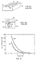
- Figure 2a is a schematic perspective view of a prior art uniform substrate with a rib waveguide section having a bend.
- Figure 2b is a schematic top view of the waveguide section of Figure 2a.
- Figure 3 is a graph of the loss associated with a 90° circular waveguide bend versus the radius of curvature of the bend for two propagation modes.
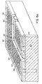
- Figure 4 is a schematic perspective view of a periodic dielectric structure having two-dimensional periodicity.
- Figure 5a is a schematic top view of the periodic dielectric structure of Figure 4 showing a triangular lattice pattern.
- Figure 5b is a schematic top view of a periodic dielectric structure showing a square lattice pattern.
- Figure 5c is a schematic top view of a periodic dielectric structure showing a hexagonal lattice pattern.
- Figure 6 is a graph of the wave attenuation in the band gap versus frequency of the wave.
- Figure 7a is a schematic perspective view of an optical circuit in accordance with the present invention.
- Figure 7b is a schematic top view of the optical circuit of Figure 7a.
- Figure 8a is a schematic perspective view of a waveguide section on a substrate having a two-dimensional periodic dielectric structure in accordance with the present invention.
- Figure 8b is a schematic top view of the device of Figure 8a.
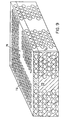
- Figure 9 is a schematic perspective view of a waveguide on a substrate having a three-dimensional periodic dielectric structure in accordance with the present invention.
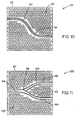
- Figure 10 is a schematic top view of an S-bend in accordance with the present invention.
- Figure 11 is a schematic top view of a Y-coupler in accordance with the present invention.
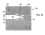
- Figure 12 is a schematic top view of a waveguide taper in accordance with the present invention.
- Optical integrated circuits and optoelectronic integrated circuits can be classified as either active or passive circuits.
- Optical integrated circuits perform a variety of passive functions, including switching and modulating, without generating or detecting light.
- Optoelectronic circuits generate and detect light as well as perform certain passive functions.
- the present invention is applicable to both types of circuits.
- optical integrated circuits optical integrated circuits
- optical circuits optical circuits
- other related terms will be used to describe the various types of circuits to which the invention is applicable. Unless otherwise specifically stated, the use of one of these terms in this application does not limit the applicability of the description to that type of circuit. One term is selected over another for illustration purposes only. The present invention is applicable to all of these circuits.
- Optical circuits can be fabricated on a top surface of a substrate.
- the optical waveguides which connect the circuits can also be fabricated on the surface of the substrate.
- These optical waveguides consist of a channel having an index of refraction which is higher than the index of refraction of the surrounding substrate. Because of the index contrast, light is guided along the channel by total internal reflection.
- Optical waveguides are used to guide optical signals among the elements in optical and optoelectronic integrated circuits and are analogous to the metallic lines used to guide electrical signals among electronic integrated circuits. They connect external optical devices such as fiber optic cables with internal optical devices such as switches, modulators, sources, and detectors. In addition, they form the basic structural elements in numerous optical devices including optical couplers, switches, modulators, power dividers, and combiners.
- Integrated optical circuits and waveguides can be implemented by several different techniques.
- a substrate 10 is made of a material such as LiNbO 3 having a low index of refraction.
- Optical circuits 11 and 13 are formed in the substrate 10 by techniques such as photolithography, diffusion, ion implantation, etching and the like.
- the optical waveguide 12 is made of a material having a high index of refraction which may be formed by diffusing titanium into the substrate 10.
- FIG. 1b Another type of integrated optical circuit and waveguide, commonly referred to as a rib waveguide, is shown in Figure 1b.
- the rib waveguide 22 connects circuits 21 and 23.
- the optical channel 22 of high refractive index is formed on the top surface of a low-refractive-index semiconductor substrate 20.
- the substrate material may be Ga x Al (1- x) As or other similar material.
- the channel 22 may be formed of GaAs or other high-refractive-index material.
- the channel 22 is formed by depositing GaAs onto the surface of the substrate 20.
- Figures 1a and 1b illustrate straight waveguide sections 12 and 22.
- Light propagating through the waveguides strikes the barrier between the interior and exterior of the waveguides at small angles. Consequently, the light is confined within the waveguides by total internal reflection.
- waveguides, at times, must include bends.
- Figure 2a schematically depicts a section of a prior art rib waveguide 32 which includes a 90° circular bend 34.
- the waveguide 32 is fabricated on the top surface 31 of a substrate 30 as described above in connection with Figure 1b.
- Figure 2b is a schematic top view of the waveguide section 32.
- the bend 34 has a radius of curvature R.
- R decreases, the angle at which light strikes the barrier 40 increases. More light escapes from the waveguide 32 causing increased bend loss.
- bend losses increase exponentially with decreasing bend radius of curvature. That is, L ⁇ ae -R/b , where L is the loss, R is the radius of curvature, and a and b are constants.
- Figure 3 is a graph of experimental data which depicts a relationship between the radius of curvature of a 90° circular waveguide bend and the loss associated with that bend. Bend loss in decibels (dB) is plotted as a function of radius of curvature in millimeters (mm) for two modes of propagation. Curve 44 is a quasi-transverse-electric mode, and curve 46 is a quasi-transverse-magnetic mode. The graph illustrates the exponential relationship between bend radius of curvature and bend loss.
- the present invention prevents light from propagating into the circuit substrate. Because the light cannot propagate into the substrate, it is confined within circuit and the waveguide.
- the substrate comprises a region which has a periodic dielectric structure.
- a periodic dielectric structure is a structure which exhibits a periodic spatial variation in dielectric constant.
- the dielectric constant is periodic in two-dimensional space within the structure.
- the structure exhibits three-dimensional spatial periodicity.
- the periodic dielectric structure is characterized by a frequency or photonic band gap, or simply a band gap.
- the band gap of a periodic dielectric structure is a band of frequencies of electromagnetic radiation which cannot propagate through the structure in the plane in which the structure exhibits periodic variation in dielectric constant.
- Figure 4 is a schematic perspective view of a periodic dielectric structure 300 illustrating two-dimensional spatial periodicity.
- the structure 300 is periodic in the x and z dimensions. Therefore, electromagnetic radiation having a frequency within the band gap of the structure cannot propagate in a plane parallel with the x-z plane, including the plane of the top surface 326 of the structure.
- the structure 300 includes a plurality of elongated elements 322 extending orthogonal to the substrate top surface 326 and bottom surface 328.
- the elements 322 are preferably cylindrically shaped and extend in a two-dimensional periodic arrangement relative to the x-z plane or any plane parallel thereto. Although cylindrical elements are described hereinafter, quasi-cylindrical elements or other shaped elongated elements may be employed. They may be formed of a non-conductive low-dielectric material disposed within a non-conductive high-dielectric substrate material 324.
- the elements 322 may simply be bores, voids, or channels which may be filled with low-dielectric fluids or solids such as air and/or other liquid or solid material.
- the elements may be formed of non-conductive high-dielectric material and may be disposed in the periodic arrangement in a non-conductive low dielectric material.
- An example of this configuration is a high-dielectric substrate with material etched away to leave only the periodic arrangement of cylindrical rods of the high-dielectric material with air in the spaces between the rods. The space may also be filled with some other low-dielectric fluid or solid.
- a longitudinal axis 325 extends through the center of each element 322 in the vertical or y-direction.
- the elements 322 are arranged periodically in two dimensions in the x-z plane which is generally orthogonal to the longitudinal axes 325 extending through the elements 322.
- the structure 300 can be positioned to filter incoming electromagnetic energy 329 polarized in any direction that is propagating in the x-z plane.
- the structure 300 reflects substantially all of the incident electromagnetic energy 329 having a frequency within the range of the photonic or frequency band gap. More specifically, electromagnetic energy within the frequency range of the band gap is substantially prevented from propagating through the structure 300.
- the structure 300 operates as a band stop filter.
- the structure maintains a substantially constant band gap frequency range for radiation propagating along any incident angle in the x-z plane.
- Figure 5a is a top view of the structure 300 of Figure 4.
- the cylindrical elements 322 are periodically arranged to provide a triangular lattice.
- the lines 327 illustrate the triangular lattice arrangement of the cylindrical elements along the top surface 326 of the substrate material 324.
- Other possible lattice structures are shown in Figures 5b and 5c.
- Figure 5b shows a square lattice structure
- Figure 5c shows a honeycomb or hexagonal lattice structure.
- a feature of the periodic dielectric structure is that the center frequency of the band gap, the bandwidth of the band gap (i.e., the stop band) and the band gap attenuation can be tailored for any frequency range in the microwave to ultraviolet bands (10 6 to 10 15 Hz) during the fabrication of the structure.
- the center frequency (f), the bandwidth ( ⁇ f) and the band gap attenuation (A G ) of the band gap are shown in Figure 6.
- the attenuation (A G ) of the band gap is proportional to the number of rows of elements 322.
- the attenuation (A G ) can be increased by providing additional rows.
- the location of the band gap on the frequency scale is determined by the center frequency.
- the bandwidth ( ⁇ f) is determined by the radius (r) of the cylindrical elements 322 and the triangular lattice constant (a).
- a two-dimensional periodic dielectric structure as shown in Figures 4 and 5a-c may be fabricated on a portion of a homogeneous or uniform substrate by one of several methods.
- One method involves drilling holes in a high- dielectric uniform substrate. The holes are filled with a low-dielectric material such as air.
- Another method involves the use of reactive-ion etching.
- the substrate is covered on one face with a mask which contains a two-dimensional array of geometric figures of the size, spacing, and periodicity required for the desired band gap.
- This two-dimensional array of geometric figures may be patterned by employing electron beam lithography or conventional photolithography.
- the geometric figures are either transparent or opaque to a reactive-ion etchant used to selectively eradicate the high dielectric substrate material. For example, if cylindrical air channels are to be formed in the substrate, the geometric figures are circles which are transparent to the etchant, and the remainder of the mask is opaque to the etchant. If square rods of high dielectric material are to be formed, the figures are squares which are opaque to the etchant, and the remainder of the mask is transparent to the etchant.
- the substrate and mask are then exposed to the highly directional reactive-ion etchant.
- the reactive-ion plasma is directed at the mask along the perpendicular axis, and vertical channels of the desired shape are created in the substrate.
- the resulting array of elements forms the two-dimensional frequency or photonic band gap.
- Figure 7a is a schematic perspective view of an integrated optical circuit 200 in accordance with the present invention.
- Figure 7b is a top view of the circuit 200.
- the circuit 200 comprises a base substrate 202 formed of a material having a low refractive index such as Ga x Al 1-x As.
- An epilayer 204 made of a material having a higher refractive index than the base substrate 202 such as GaAs is formed on the top surface of the base substrate 202.
- the combination of the base substrate 202 and the epilayer 204 forms the substrate 206 for the optical circuit 200.
- the components of the optical circuit 200 include two optical devices 208 and 210. These devices may be a laser and a detector or other similar devices. It will be understood that the invention is applicable to other such devices. Also, two devices are selected for ease of description only. Typical circuits will have more devices.
- the devices 208 and 210 are connected by a waveguide 212.
- the waveguide 212 includes a straight section 214, a bend 216 and a second straight section 218.
- light is assumed to leave device 208 and propagate through the waveguide 212 toward device 210.
- the light passes through straight section 214, bend 216 and straight section 218 and enters device 210.
- the optical devices 208 and 210 are surrounded by periodic dielectric structure 222.
- the periodic dielectric structure 222 prevents emissions from the devices 208 and 210 at a frequency within the band gap of the structure 222 from propagating into the substrate 206.
- the devices 208 and 210 are isolated from each other, the waveguide 212, and any other devices on the substrate 206.
- the periodic dielectric structure 222 also serves to define the lateral extents of the waveguide 212 on the epilayer 204.
- the periodic dielectric structure 222 prevents light at a frequency within the band gap of the structure 222 from propagating in the plane of the epilayer 204. Thus, the light is confined laterally within the waveguide 212. Light is prevented from propagating out of the waveguide 212 in the vertical directions by internal reflection. Light will not propagate up out of the waveguide into space because of the refractive index contrast between the interior of the waveguide and the air above it. Light will not propagate down into the base substrate 202 because of the index contrast between the epilayer 204 and the base substrate 202. Because the light cannot propagate outside the waveguide 212, it is confined inside. The light entering the waveguide 212 from the device 208 travels through the straight section 214 into bend 216. It is guided around the bend 216 by the periodic dielectric structure 222 and through straight section 218 into device 210.
- the circuit 200 of Figures 7a and 7b is made by first forming the uniform high-refractive-index epilayer 204 on top of a uniform low-refractive index base substrate 202 to form substrate 206. This is done by diffusion or similar fabrication technique. Next, the devices 208 and 210 are formed on the epilayer 204. Finally, the periodic dielectric structure 222 is formed in the substrate 206 by one of the methods previously described.
- the periodic dielectric structure 222 is designed to create a frequency band gap for the substrate 206 which includes the frequency of the radiation which will be carried by the waveguide 212.
- the periodic pattern of holes is formed in the substrate 206.
- the pattern of holes is made to surround devices 208 and 210 and to define the waveguide 212 connecting the devices.
- the holes are made by either drilling or by the reaction ion etching process previously described.
- Figures 8a and 8b depict a section of waveguide 56 in accordance with another embodiment of the invention.
- a high-refractive-index epilayer 51 made of a material such as GaAs is formed on the top surface of a low-refractive-index base substrate 50 made of a material such as Ga x Al 1-x As to form a substrate 53.
- the substrate 53 may also be made of other materials such as dielectric or optical materials.
- the periodic dielectric structure 52 is periodic in two dimensions in the plane of the epilayer 51.
- the section of optical waveguide 56 is formed in the epilayer 51 between substantially parallel trenches 58 and 60.
- the waveguide section 56 includes a 90° circular bend 62. The 90° bend angle is chosen for illustration purposes only. The bend angle need not be 90°.
- the trenches 58 and 60 are formed by etching or other known processes.
- the air in the trenches provides refractive index contrast for internal reflection of the light carried by the waveguide 56.
- Periodic dielectric structure 52 is provided outside the trenches 58 and 60 to eliminate loss where the requirements for total internal reflection are not met.
- the periodic dielectric structure 52 is formed as described in connection with Figures 4-6 to have a frequency band gap at the known frequency of the light propagating in the waveguide 56. Therefore, the light cannot propagate into the substrate 53 in the plane of the epilayer 51. As a result, loss of light at the bend 62 is virtually eliminated.
- the waveguide 56 is formed by creating the trenches 58 and 60 in the epilayer 51.
- Other methods are also possible, including those previously described in connection with Figures 1a and 1b.
- a high-refractive-index channel may be formed by diffusing material into a uniform substrate or etching material onto the substrate. After the channel is formed, the periodic dielectric structure is formed in the substrate by the procedure previously described.
- Figure 9 illustrates a waveguide section 76 in accordance with another embodiment of the present invention.
- the substrate 70 includes a high-refractive-index epilayer 71 and a lower-refractive-index base substrate 73.
- the substrate 70 also comprises a periodic dielectric structure 72 having three-dimensional spatial periodicity. Radiation is prevented from propagating in all three spatial dimensions of the substrate 70.
- the three-dimensional periodic dielectric structure 72 is fabricated in a similar manner to the two-dimensional structure.
- the epilayer 71 is covered with a mask having a two-dimensional array of geometric figures defining the desired pattern for the top surface of the three-dimensional periodic dielectric structure.
- the two-dimensional array has a triangular lattice pattern.
- the substrate and mask are exposed to the reactive-ion etchant.
- the etchant plasma is directed successively at three different angles with respect to the axis perpendicular to the top surface of the substrate. The angles are each oriented down 35.26° from the perpendicular and are separated by 120° from each other in azimuth.
- the resulting channels form a three-dimensional face-centered cubic lattice.
- the electromagnetic dispersion relation in this lattice will exhibit a photonic or frequency band gap.
- the periodic dielectric structure 72 prevents propagation of light within the band gap in all three dimensions. Light cannot propagate laterally through the substrate 72 as in the two-dimensional case. But also, it cannot propagate toward the bottom surface 75 of the substrate 70. Optical losses are further reduced.
- FIGS 10-12 illustrate various optical circuits to which the present invention is applicable.
- Each figure is a top view of a portion of a substrate on which is formed a device in accordance with the invention.
- the periodic dielectric structure used in each device may have either two-dimensional or three-dimensional periodicity.
- Figure 10 is a view of an S-bend device 93 in a waveguide section.
- the S-bend 93 is used in such devices as optical couplers. It includes two bend sections 90 and 91. In prior devices with uniform substrates, these bends would be sources of radiation loss. However, because the bends are surrounded by a periodic dielectric structure 92 in the substrate 87, the bend losses ae virtually eliminated.
- Figure 11 is a view of a Y-coupler device 103.
- An incoming signal enters the device 103 through straight section 94.
- the signal is split at junction 96 into two equal outgoing signals traveling through sections 98 and 99. Radiation losses associated with the junction 96 and bends 100 and 101 are virtually eliminated by the periodic dielectric structure 102 in the substrate 97. It should be noted that where radiation propagates from right to left in Figure 11, the device 103 serves a combiner.
- Figure 12 shows a waveguide taper or funnel 110 on a substrate 102 with a periodic dielectric structure 104.
- Many applications require a fiber optic cable 112 to be permanently attached to a waveguide 114 on an optical integrated circuit. This connection can lead to insertion loss on the order of 10dB.
- the cable end 116 of the integrated waveguide 114 is made the same width as the cable 112.
- the optimum width of the circuit end 118 of the waveguide 114 is less than the width of the cable end 116.
- the width transition between the two ends is made of a taper section 120. This taper section 120 is a source of loss which can be overcome by the periodic dielectric structure 104.
Claims (23)
- Ein Verfahren zur Bildung optischer Schaltkreise, das folgendes umfasst:Bereitstellen einer Unterlage (202), zum Beispiel eines Halbleiter-Materials; undBilden eines optischen Schaltkreises (208, 210, 212), der zum Beispiel einen Laser enthält, auf oder in der Unterlage; gekennzeichnet dadurch, dassdie Methode außerdem den Schritt zur Bildung eines Bereiches der Unterlage mit einer periodischen dielektrischen Gitterstruktur (222) umfasst, welche eine räumlich periodische Variation in dielektrischer Konstanz in mindestens zwei Dimensionen hat, wobei die Dimensionen des Gitters so proportioniert sind, dass sie einen Frequenzbandabstand produzieren, der ein Band von Frequenzen von elektromagnetischer Strahlung definiert, bei dem der optische Schaltkreis betriebsfähig ist, und die Gitterstruktur (222) ausreichend nahe an dem optischen Schaltkreis angeordnet ist, so dass in einer Ebene der periodischen Variation, das Entweichen von Strahlung aus dem optischen Schaltkreis bei solchen Frequenzen wesentlich verhindert wird.
- Das Verfahren nach Anspruch 1, worin der Bereich gebildet wird als Teil des oder anliegend an den optischen Schaltkreis.
- Das Verfahren nach einem beliebigen vorausgegangenen Anspruch, worin die periodische dielektrische Gitterstruktur eine zweidimensionale oder dreidimensionale dielektrische periodische Gitterstruktur (222:72) ist.
- Das Verfahren nach einem beliebigen vorausgegangenen Anspruch, worin der Schritt zur Bildung des optischen Schaltkreises das Bilden eines optischen Wellenleiters (212) auf oder in der Unterlage umfasst.
- Das Verfahren nach Anspruch 4, worin der Bereich mit der periodischen dielektrischen Gitterstruktur anliegend an eine Krümmung (216) oder anliegend an eine Verjüngung (120) in dem Wellenleiter gebildet wird, so dass die Strahlungsverluste, die in Verbindung mit der Krümmung oder der Verjüngung stehen, reduziert werden.
- Ein Verfahren nach einem beliebigen vorausgegangenen Anspruch, worin der optische Schaltkreis ein optischer integrierter Schaltkreis oder ein opto-elektronischer Schaltkreis ist.
- Ein optisches Gerät mit reduzierten Strahlungsverlusten, das umfasst:eine Unterlage (202), zum Beispiel ein Halbleiter-Material; undeinen optischen Schaltkreis (208, 210, 212), der zum Beispiel einen optischen Wellenleiter (212) umfasst, der auf oder in der Unterlage gebildet wurde; gekennzeichnet dadurch, dass das optische Gerät außerdem einen Bereich umfasst, der auf oder in der Unterlage gebildet wurde, und eine periodische dielektrische Gitterstruktur (222) hat mit räumlichen periodischen Variationen in dielektrischer Konstanz in mindestens zwei Dimensionen, wobei die Dimensionen des Gitters so proportioniert sind, dass sie einen Frequenzbandabstand produzieren, der ein Band von Frequenzen von elektromagnetischer Strahlung definiert, bei dem der optische Schaltkreis betriebsfähig ist, und die Gitterstruktur (222) ausreichend nahe an dem optischen Schaltkreis angeordnet ist, so dass in einer Ebene der periodischen Variation, das Entweichen von Strahlung aus dem optischen Schaltkreis bei solchen Frequenzen wesentlich verhindert wird.
- Das optische Gerät nach Anspruch 7, worin der Bereich ein Teil von bzw. ein Teil anliegend an den optischen Schaltkreis ist.
- Das optische Gerät nach einem der vorausgegangenen Ansprüche 7 oder 8, worin die periodische dielektrische Gitterstruktur eine zweidimensionale oder dreidimensionale periodische dielektrische Gitterstruktur (222:72) ist.
- Das optische Gerät nach einem beliebigen der vorausgegangenen Ansprüche 7 bis 9, worin der optische Schaltkreis einen optischen Wellenleiter (212) umfasst und, worin optional, der Bereich anliegend an eine Krümmung (216) oder anliegend an eine Verjüngung (120) in dem Wellenleiter gebildet wird, so dass die Strahlungsverluste, die in Verbindung mit der Krümmung oder der Verjüngung stehen, reduziert werden.
- Das optische Gerät nach einem der Ansprüche 7 bis 10, worin der optische Schaltkreis einen optischen Wellenleiter umfasst, der ein Kanal in der Unterlage ist, umgeben von dem Bereich, der die periodische dielektrische Gitterstruktur hat.
- Das optische Gerät nach einem der Ansprüche 7 bis 11, worin der optische Schaltkreis ein optischer integrierter Schaltkreis oder ein opto-elektronischer Schaltkreis ist.
- Ein Verfahren zur Bildung eines optischen Wellenleiters, das umfasst:Bereitstellen einer Unterlage (202), zum Beispiel eines Halbleiter-Materials; undBilden eines optischen Wellenleiters auf oder in der Unterlage; gekennzeichnet dadurch dass,die Methode außerdem den Schritt zur Bildung eines Bereiches der Unterlage mit einer periodischen dielektrischen Gitterstruktur (222) umfasst, welche eine räumlich periodische Variation in dielektrischer Konstanz in mindestens zwei Dimensionen hat, wobei die Dimensionen des Gitters so proportioniert sind, dass sie einen Frequenzbandabstand produzieren, der ein Band von Frequenzen von elektromagnetischer Strahlung definiert, bei dem der optische Wellenleiter betriebsfähig ist, und die Gitterstruktur (222) ausreichend nahe an dem optischen Wellenleiter angeordnet ist, so dass in einer Ebene der periodischen Variation, das Entweichen von Strahlung aus dem optischen Wellenleiter bei solchen Frequenzen wesentlich verhindert wird.
- Das Verfahren nach Anspruch 13, worin der Wellenleiter eine Krümmung umfasst.
- Das Verfahren nach Anspruch 13, worin der Wellenleiter eine Verjüngung umfasst.
- Das Verfahren nach Anspruch 13, worin die periodische dielektrische Struktur eine zweidimensionale periodische dielektrische Struktur ist.
- Das Verfahren nach Anspruch 13, worin die periodische dielektrische Struktur eine dreidimensionale periodische dielektrische Struktur ist.
- Das Verfahren nach Anspruch 13, worin die Unterlage ein Halbleiter-Material umfasst.
- Das Verfahren nach Anspruch 13, worin der Schritt zur Bildung eines Bereichs die Bildung eines periodischen Musters von leeren Bereichen in der Unterlage umfasst.
- Das Verfahren nach Anspruch 13, worin der Schritt zur Bildung eines optischen Wellenleiters die Verhinderung der Bildung des Bereichs mit dem Frequenzbandabstand in einem bestimmten Teil der Unterlage umfasst, wobei der genannte Teil der Unterlage der optische Wellenleiter ist.
- Das Verfahren nach Anspruch 13, worin der Schritt zur Bildung eines optischen Wellenleiters das Verbreiten eines Materials in der Unterlage umfasst, wobei das genannte Material einen Refraktionskoeffizienten hat, der höher als der Refraktionskoeffizient der Unterlage ist.
- Das Verfahren nach Anspruch 13, worin der Schritt zur Bildung eines optischen Wellenleiters das Ablagern eines Materials auf einer Oberfläche der Unterlage umfasst, wobei das genannte Material einen Refraktionskoeffizienten hat, der höher als der Refraktionskoeffizient der Unterlage ist.
- Das Verfahren nach Anspruch 13, worin der Schritt zur Bildung eines optischen Wellenleiters die Bildung von zwei im wesentlichen parallelen Rinnen in einer Oberfläche der Unterlage umfasst, wobei die genannten Rinnen einen Materialkanal zwischen ihnen definieren und der genannte Materialkanal der optische Wellenleiter ist.
Applications Claiming Priority (3)
| Application Number | Priority Date | Filing Date | Title |
|---|---|---|---|
| US243093A | 1993-01-08 | 1993-01-08 | |
| US2430 | 1993-01-08 | ||
| PCT/US1994/000285 WO1994016345A1 (en) | 1993-01-08 | 1994-01-07 | Low-loss optical and optoelectronic integrated circuits |
Publications (2)
| Publication Number | Publication Date |
|---|---|
| EP0678196A1 EP0678196A1 (de) | 1995-10-25 |
| EP0678196B1 true EP0678196B1 (de) | 2002-04-10 |
Family
ID=21700730
Family Applications (1)
| Application Number | Title | Priority Date | Filing Date |
|---|---|---|---|
| EP94906565A Expired - Lifetime EP0678196B1 (de) | 1993-01-08 | 1994-01-07 | Verlustarme optische und optoelektronische integrierte schaltungen |
Country Status (6)
| Country | Link |
|---|---|
| US (1) | US5526449A (de) |
| EP (1) | EP0678196B1 (de) |
| JP (1) | JPH08505707A (de) |
| CA (1) | CA2153485A1 (de) |
| DE (1) | DE69430361D1 (de) |
| WO (1) | WO1994016345A1 (de) |
Cited By (1)
| Publication number | Priority date | Publication date | Assignee | Title |
|---|---|---|---|---|
| EP2657649A3 (de) * | 2006-09-27 | 2015-08-26 | Northrop Grumman Systems Corporation | Photonischer Rotationssensor auf Kristallbasis |
Families Citing this family (136)
| Publication number | Priority date | Publication date | Assignee | Title |
|---|---|---|---|---|
| WO1996011516A1 (en) * | 1994-10-05 | 1996-04-18 | Massachusetts Institute Of Technology | Resonant microcavities employing one-dimensional periodic dielectric waveguides |
| US5784400A (en) * | 1995-02-28 | 1998-07-21 | Massachusetts Institute Of Technology | Resonant cavities employing two dimensionally periodic dielectric materials |
| FR2734097B1 (fr) * | 1995-05-12 | 1997-06-06 | Thomson Csf | Laser a semiconducteurs |
| US5790583A (en) * | 1995-05-25 | 1998-08-04 | Northwestern University | Photonic-well Microcavity light emitting devices |
| US5878070A (en) * | 1995-05-25 | 1999-03-02 | Northwestern University | Photonic wire microcavity light emitting devices |
| US5825799A (en) * | 1995-05-25 | 1998-10-20 | Northwestern University | Microcavity semiconductor laser |
| DE19520819A1 (de) * | 1995-05-30 | 1996-12-05 | Deutsche Telekom Ag | Verfahren zur Ausnutzung scheibenförmigen Ausgangsmaterials bei der Herstellung optoelektronischer Bauelemente mit Gittern variabler Gitterperiode |
| US5747796A (en) * | 1995-07-13 | 1998-05-05 | Sharp Kabushiki Kaisha | Waveguide type compact optical scanner and manufacturing method thereof |
| JPH09145943A (ja) * | 1995-11-28 | 1997-06-06 | Mitsubishi Gas Chem Co Inc | 曲がり光導波路およびその製造法 |
| US6052213A (en) * | 1996-03-27 | 2000-04-18 | British Telecommunications Plc | Optical diffraction grating |
| US6002522A (en) * | 1996-06-11 | 1999-12-14 | Kabushiki Kaisha Toshiba | Optical functional element comprising photonic crystal |
| US5955749A (en) * | 1996-12-02 | 1999-09-21 | Massachusetts Institute Of Technology | Light emitting device utilizing a periodic dielectric structure |
| WO1998035248A1 (en) | 1997-02-11 | 1998-08-13 | Massachusetts Institute Of Technology | Polymeric photonic band gap materials |
| US6483640B1 (en) * | 1997-04-08 | 2002-11-19 | The United States Of America As Represented By The Secretary Of The Navy | Optical notch filters based on two-dimensional photonic band-gap materials |
| GB9710062D0 (en) * | 1997-05-16 | 1997-07-09 | British Tech Group | Optical devices and methods of fabrication thereof |
| US6735368B2 (en) | 1997-05-16 | 2004-05-11 | Mesophotonics Limited | Optical delay device |
| US6788863B2 (en) | 1997-05-16 | 2004-09-07 | Mesophotonics Limited | Optical delay device |
| US6134372A (en) * | 1997-10-01 | 2000-10-17 | Sumitomo Osaka Cement Co., Ltd. | Light intensity attenuator and attenuating method |
| IL123207A0 (en) * | 1998-02-06 | 1998-09-24 | Shellcase Ltd | Integrated circuit device |
| WO2002051217A2 (en) * | 2000-12-21 | 2002-06-27 | Shellcase Ltd. | Packaged integrated circuits and methods of producing thereof |
| DE69923292T2 (de) | 1998-02-19 | 2006-03-23 | Massachusetts Institute Of Technology, Cambridge | Omnidirektionaler reflektor aus photonischem kristall |
| US5999308A (en) * | 1998-04-01 | 1999-12-07 | Massachusetts Institute Of Technology | Methods and systems for introducing electromagnetic radiation into photonic crystals |
| GB2334789B (en) * | 1998-06-12 | 2000-01-19 | Bookham Technology Ltd | A waveguide end face |
| AU4967499A (en) | 1998-07-02 | 2000-01-24 | Massachusetts Institute Of Technology | Periodic porous and relief nanostructured articles |
| JP3522117B2 (ja) * | 1998-08-05 | 2004-04-26 | 日本電気株式会社 | 自己導波光回路 |
| US6134043A (en) * | 1998-08-11 | 2000-10-17 | Massachusetts Institute Of Technology | Composite photonic crystals |
| US6175671B1 (en) * | 1998-10-01 | 2001-01-16 | Nortel Networks Limited | Photonic crystal waveguide arrays |
| US6463200B2 (en) | 1998-10-14 | 2002-10-08 | Massachusetts Institute Of Technology | Omnidirectional multilayer device for enhanced optical waveguiding |
| ATE243853T1 (de) * | 1999-05-21 | 2003-07-15 | British Telecomm | Planare optische wellenleiter mit zwei nuten |
| EP1058135A1 (de) * | 1999-05-21 | 2000-12-06 | BRITISH TELECOMMUNICATIONS public limited company | Planarer optischer Siliziumdioxid Wellenleiter zwischen zwei Nuten |
| JP3456166B2 (ja) * | 1999-06-23 | 2003-10-14 | 日本電気株式会社 | フォトニック結晶を用いた光結合素子および光結合方法 |
| JP3980801B2 (ja) * | 1999-09-16 | 2007-09-26 | 株式会社東芝 | 三次元構造体およびその製造方法 |
| US6468823B1 (en) * | 1999-09-30 | 2002-10-22 | California Institute Of Technology | Fabrication of optical devices based on two dimensional photonic crystal structures and apparatus made thereby |
| EP1109038A1 (de) * | 1999-12-17 | 2001-06-20 | Corning Incorporated | Verfahren zum Herstellen einer integrierten optischen Schaltung |
| JP4161498B2 (ja) | 1999-12-28 | 2008-10-08 | コニカミノルタホールディングス株式会社 | 光モジュールの製造方法 |
| JP2001281714A (ja) | 2000-01-24 | 2001-10-10 | Minolta Co Ltd | 光機能素子及び光集積化素子 |
| WO2001067607A2 (en) * | 2000-03-10 | 2001-09-13 | Romaniuk Charles C | Dynamic phase logic gate |
| JP3925769B2 (ja) * | 2000-03-24 | 2007-06-06 | 関西ティー・エル・オー株式会社 | 2次元フォトニック結晶及び合分波器 |
| JP2001281480A (ja) * | 2000-03-29 | 2001-10-10 | Nec Corp | フォトニック結晶光導波路と方向性結合器 |
| US6463202B1 (en) | 2000-06-09 | 2002-10-08 | Southwest Research Institute | Optimization of curved waveguide design to reduce transmission losses |
| AU2002218750A1 (en) * | 2000-07-06 | 2002-01-21 | Massachusetts Institute Of Technology | Photoactivated drug therapy |
| US6684008B2 (en) * | 2000-09-01 | 2004-01-27 | The University Of British Columbia | Planar photonic bandgap structures for controlling radiation loss |
| GB0023478D0 (en) * | 2000-09-25 | 2000-11-08 | Marconi Caswell Ltd | Artifically structured dielectric material |
| JP3586635B2 (ja) * | 2000-10-19 | 2004-11-10 | 株式会社日立製作所 | 光デバイスおよび基板 |
| JP2002169052A (ja) * | 2000-11-30 | 2002-06-14 | Japan Aviation Electronics Industry Ltd | 異方導光性部材を有する光学装置 |
| US6383924B1 (en) * | 2000-12-13 | 2002-05-07 | Micron Technology, Inc. | Method of forming buried conductor patterns by surface transformation of empty spaces in solid state materials |
| JP4446591B2 (ja) * | 2000-12-20 | 2010-04-07 | 京セラ株式会社 | 光導波路および光回路基板 |
| WO2002056430A2 (en) * | 2001-01-11 | 2002-07-18 | California Institute Of Technology | A compact electrically and optically pumped multi-wavelength nanocavity laser, modulator and detector arrays and method of making the same |
| EP1366383A1 (de) | 2001-01-25 | 2003-12-03 | Omniguide Communications Inc. | Photonische kristalllichtwellenleiter mit angepassten dispersionsprofilen |
| JP2004521378A (ja) | 2001-01-25 | 2004-07-15 | オムニガイド コミュニケーションズ インコーポレイテッド | 大きいコア半径を有する低損失フォトニック結晶導波路 |
| JP2004521379A (ja) | 2001-01-31 | 2004-07-15 | オムニガイド コミュニケーションズ インコーポレイテッド | フォトニック結晶多モード導波路の電磁モード変換 |
| DE10104563A1 (de) * | 2001-02-01 | 2002-08-22 | Infineon Technologies Ag | Halbleiterelement mit optoelektronischer Signalübertragung und Verfahren zum Erzeugen eines solchen Halbleiterelements |
| JP2002303836A (ja) * | 2001-04-04 | 2002-10-18 | Nec Corp | フォトニック結晶構造を有する光スイッチ |
| CA2443127A1 (en) | 2001-04-12 | 2002-10-24 | Wesley King | High index-contrast fiber waveguides and applications |
| US6574383B1 (en) | 2001-04-30 | 2003-06-03 | Massachusetts Institute Of Technology | Input light coupler using a pattern of dielectric contrast distributed in at least two dimensions |
| US6936854B2 (en) | 2001-05-10 | 2005-08-30 | Canon Kabushiki Kaisha | Optoelectronic substrate |
| US6917431B2 (en) * | 2001-05-15 | 2005-07-12 | Massachusetts Institute Of Technology | Mach-Zehnder interferometer using photonic band gap crystals |
| US7142577B2 (en) * | 2001-05-16 | 2006-11-28 | Micron Technology, Inc. | Method of forming mirrors by surface transformation of empty spaces in solid state materials and structures thereon |
| US6898362B2 (en) * | 2002-01-17 | 2005-05-24 | Micron Technology Inc. | Three-dimensional photonic crystal waveguide structure and method |
| US7018467B2 (en) * | 2002-01-17 | 2006-03-28 | Micron Technology, Inc. | Three-dimensional complete bandgap photonic crystal formed by crystal modification |
| US6582512B2 (en) * | 2001-05-22 | 2003-06-24 | Micron Technology, Inc. | Method of forming three-dimensional photonic band structures in solid materials |
| DE10132850A1 (de) * | 2001-07-06 | 2003-01-23 | Fraunhofer Ges Forschung | Ablenkeinrichtung und Verfahren zur Ablenkung elektromagnetischer Wellen und optisches Element hierfür, sowie Verfahren zur Herstellung photonischer Strukturen |
| JP3743637B2 (ja) * | 2001-08-23 | 2006-02-08 | 独立行政法人理化学研究所 | フォトニック結晶および光導波素子 |
| US6856007B2 (en) | 2001-08-28 | 2005-02-15 | Tessera, Inc. | High-frequency chip packages |
| US6707597B2 (en) * | 2001-09-17 | 2004-03-16 | Matsushita Electric Industrial Co., Ltd. | Optical device and method for producing photonic crystal |
| KR100394019B1 (ko) * | 2001-09-29 | 2003-08-09 | 엘지전자 주식회사 | 광통신용 커플러 소자의 제조 방법 |
| KR100394018B1 (ko) * | 2001-09-29 | 2003-08-09 | 엘지전자 주식회사 | 광통신용 슈퍼 광학 프리즘 제조 방법 |
| WO2003034118A1 (en) * | 2001-10-17 | 2003-04-24 | Risø National Laboratory | A system for electromagnetic field conversion |
| JP2003149479A (ja) * | 2001-11-14 | 2003-05-21 | Hitachi Cable Ltd | 石英系ガラス光導波路及びそれを用いた光モジュール |
| US20030133661A1 (en) * | 2002-01-16 | 2003-07-17 | Ali Adibi | Use of tapered dielectric slab waveguides for input and output coupling of light into photonic crystal devices |
| US20040176483A1 (en) * | 2003-03-05 | 2004-09-09 | Micron Technology, Inc. | Cellular materials formed using surface transformation |
| KR100670080B1 (ko) * | 2002-01-17 | 2007-01-17 | 마이크론 테크놀로지, 인크. | 3차원 광자 결정 도파관 구조 |
| GB2384319A (en) * | 2002-01-19 | 2003-07-23 | Marconi Optical Components Ltd | Polarisation converter for photonic crystal waveguide |
| FR2837003B1 (fr) * | 2002-03-05 | 2004-06-04 | Cit Alcatel | Dispositif optique comportant un adaptateur de mode sur composant optique a bande interdite photonique |
| EP1481272A1 (de) * | 2002-03-06 | 2004-12-01 | Pirelli & C. S.p.A. | Einrichtung zum beugen eines optischen strahls insbesondere in einer optischen integrierten schaltung |
| WO2003075056A1 (en) * | 2002-03-06 | 2003-09-12 | Pirelli & C. S.P.A. | Device for crossing optical beams, in particular in an integrated optical circuit |
| AU2002254928A1 (en) * | 2002-03-06 | 2003-09-16 | Pirelli & C. S.P.A. | Method for guiding an electromagnetic radiation, in particular in an integrated optical device |
| FR2841658B1 (fr) * | 2002-06-26 | 2004-10-22 | Centre Nat Rech Scient | Dispositif de couplage optique directionnel et selectif en longueur d'onde |
| US6957003B2 (en) * | 2002-06-27 | 2005-10-18 | The Board Of Trustees Of The Leland Stanford Junior University | Creating large bandwidth line defects by embedding dielectric waveguides into photonic crystal slabs |
| US20040013384A1 (en) * | 2002-07-17 | 2004-01-22 | Greg Parker | Optical waveguide structure |
| US7319709B2 (en) | 2002-07-23 | 2008-01-15 | Massachusetts Institute Of Technology | Creating photon atoms |
| US6944373B2 (en) * | 2002-08-01 | 2005-09-13 | Northrop Grumman Corporation | High index-step grating fabrication using a regrowth-over-dielectric process |
| US20040086244A1 (en) | 2002-11-05 | 2004-05-06 | Zoorob Majd E. | Optical waveguide structure |
| DE10254909B4 (de) | 2002-11-25 | 2004-10-07 | Infineon Technologies Ag | Abstimmbarer Halbleiterlaser und Herstellungsverfahren |
| US6832029B2 (en) * | 2002-12-17 | 2004-12-14 | Mcnc | Impedance control devices for use in the transition regions of electromagnetic and optical circuitry and methods for using the same |
| US6709969B1 (en) * | 2002-12-19 | 2004-03-23 | Mark E. Murray | Method for fabricating a gas insulated gate field effect transistor |
| US7273788B2 (en) * | 2003-05-21 | 2007-09-25 | Micron Technology, Inc. | Ultra-thin semiconductors bonded on glass substrates |
| US7008854B2 (en) * | 2003-05-21 | 2006-03-07 | Micron Technology, Inc. | Silicon oxycarbide substrates for bonded silicon on insulator |
| US20040240784A1 (en) * | 2003-05-30 | 2004-12-02 | General Electric Company | Apparatus for coupling electromagnetic energy and method of making |
| US6972480B2 (en) * | 2003-06-16 | 2005-12-06 | Shellcase Ltd. | Methods and apparatus for packaging integrated circuit devices |
| CN100587962C (zh) | 2003-07-03 | 2010-02-03 | 泰塞拉技术匈牙利公司 | 用于封装集成电路器件的方法和设备 |
| US6929984B2 (en) * | 2003-07-21 | 2005-08-16 | Micron Technology Inc. | Gettering using voids formed by surface transformation |
| JP2005045162A (ja) * | 2003-07-25 | 2005-02-17 | Mitsubishi Electric Corp | 半導体素子およびその製造方法 |
| US7224056B2 (en) | 2003-09-26 | 2007-05-29 | Tessera, Inc. | Back-face and edge interconnects for lidded package |
| US7068865B2 (en) * | 2003-10-15 | 2006-06-27 | International Business Machines Corporation | Method and apparatus for thermo-optic modulation of optical signals |
| US8606060B2 (en) * | 2003-10-15 | 2013-12-10 | International Business Machines Corporation | Method and apparatus for dynamic manipulation and dispersion in photonic crystal devices |
| US20050084195A1 (en) * | 2003-10-15 | 2005-04-21 | Hamann Hendrik F. | Method and apparatus for forming lateral electrical contacts for photonic crystal devices |
| US6996317B2 (en) * | 2003-10-23 | 2006-02-07 | Fitel U.S.A. Corp. | Optical devices including microstructured fiber sections disposed for transverse signal propagation |
| US7218812B2 (en) * | 2003-10-27 | 2007-05-15 | Rpo Pty Limited | Planar waveguide with patterned cladding and method for producing the same |
| WO2005045512A1 (ja) * | 2003-11-10 | 2005-05-19 | Matsushita Electric Industrial Co., Ltd. | 光変調素子及び通信システム |
| WO2005052662A1 (en) * | 2003-11-28 | 2005-06-09 | Mcgill University | Wavelength multiplexer/demultiplexer comprising an optically dispersive stratified body |
| US20050124712A1 (en) * | 2003-12-05 | 2005-06-09 | 3M Innovative Properties Company | Process for producing photonic crystals |
| DE60328835D1 (de) * | 2003-12-05 | 2009-09-24 | 3M Innovative Properties Co | Prozess zur herstellung von photonischen kristallen |
| US7228042B2 (en) * | 2005-03-04 | 2007-06-05 | International Business Machines Corporation | Method and apparatus for resonant coupling in photonic crystal circuits |
| WO2006100905A1 (ja) * | 2005-03-18 | 2006-09-28 | Kyoto University | 偏波モード変換器 |
| US8143095B2 (en) | 2005-03-22 | 2012-03-27 | Tessera, Inc. | Sequential fabrication of vertical conductive interconnects in capped chips |
| EP1910875A4 (de) | 2005-07-08 | 2013-08-14 | Univ Princeton | Quasikristallinstrukturen und ihre verwendungen |
| US7566853B2 (en) * | 2005-08-12 | 2009-07-28 | Tessera, Inc. | Image sensor employing a plurality of photodetector arrays and/or rear-illuminated architecture |
| US9530940B2 (en) | 2005-10-19 | 2016-12-27 | Epistar Corporation | Light-emitting device with high light extraction |
| TWI451597B (zh) * | 2010-10-29 | 2014-09-01 | Epistar Corp | 光電元件及其製造方法 |
| US7936062B2 (en) | 2006-01-23 | 2011-05-03 | Tessera Technologies Ireland Limited | Wafer level chip packaging |
| US20080024786A1 (en) * | 2006-07-31 | 2008-01-31 | Honeywell International, Inc. | Fiber optic gyroscope having a silicon-based optical chip |
| US8604605B2 (en) | 2007-01-05 | 2013-12-10 | Invensas Corp. | Microelectronic assembly with multi-layer support structure |
| US8755658B2 (en) * | 2007-02-15 | 2014-06-17 | Institut National D'optique | Archimedean-lattice microstructured optical fiber |
| TWI355046B (en) * | 2007-07-10 | 2011-12-21 | Nanya Technology Corp | Two bit memory structure and method of making the |
| US8121487B2 (en) * | 2008-02-05 | 2012-02-21 | Honeywell International Inc. | System and method for free space micro machined optical bench |
| US7991289B2 (en) * | 2008-03-28 | 2011-08-02 | Raytheon Company | High bandwidth communication system and method |
| US8682128B2 (en) * | 2008-08-21 | 2014-03-25 | International Business Machines Corporation | Optical waveguide with periodic sub-wavelength sized regions |
| WO2010025423A2 (en) * | 2008-08-28 | 2010-03-04 | The Board Of Regents, The University Of Texas System | Multimode interference coupler for use with slot photonic crystal waveguides |
| CN102144179B (zh) * | 2008-09-04 | 2013-06-12 | 惠普开发有限公司 | 损耗得以减少的介电波导相交点 |
| US8946736B2 (en) | 2010-10-29 | 2015-02-03 | Epistar Corporation | Optoelectronic device and method for manufacturing the same |
| US9070827B2 (en) | 2010-10-29 | 2015-06-30 | Epistar Corporation | Optoelectronic device and method for manufacturing the same |
| DE102010004442B4 (de) * | 2010-01-13 | 2015-08-20 | Leoni Kabel Holding Gmbh | Optisches Bauelement zur Lichtwellenleitung, optisches Steckverbindungssystem mit einem solchen Bauelement und Verfahren zur Herstellung eines solchen Bauelements |
| US9240671B2 (en) * | 2011-11-07 | 2016-01-19 | Citizen Holdings Co., Ltd. | Laser light source |
| US9952388B2 (en) * | 2012-09-16 | 2018-04-24 | Shalom Wertsberger | Nano-scale continuous resonance trap refractor based splitter, combiner, and reflector |
| US9581762B2 (en) | 2012-09-16 | 2017-02-28 | Shalom Wertsberger | Pixel structure using a tapered core waveguide, image sensors and camera using same |
| US9823415B2 (en) | 2012-09-16 | 2017-11-21 | CRTRIX Technologies | Energy conversion cells using tapered waveguide spectral splitters |
| US9888283B2 (en) | 2013-03-13 | 2018-02-06 | Nagrastar Llc | Systems and methods for performing transport I/O |
| USD758372S1 (en) | 2013-03-13 | 2016-06-07 | Nagrastar Llc | Smart card interface |
| US9535308B2 (en) * | 2013-09-25 | 2017-01-03 | Oracle International Corporation | Enhanced optical modulation using slow light |
| CN104360439B (zh) * | 2014-11-28 | 2019-01-01 | 南京信息工程大学 | 一种基于变换介质的光子晶体弯折波导结构 |
| USD864968S1 (en) | 2015-04-30 | 2019-10-29 | Echostar Technologies L.L.C. | Smart card interface |
| US10908431B2 (en) | 2016-06-06 | 2021-02-02 | Shalom Wertsberger | Nano-scale conical traps based splitter, combiner, and reflector, and applications utilizing same |
| CN107678091A (zh) * | 2017-11-20 | 2018-02-09 | 中山大学 | 一种紧凑的光波导交叉耦合器 |
| US11163114B2 (en) | 2019-08-23 | 2021-11-02 | Globalfoundries U.S. Inc. | Waveguide structures |
| US11243071B2 (en) * | 2020-02-03 | 2022-02-08 | The Boeing Company | Sub-surface patterning for diffraction-based strain measurement and damage detection in structures |
Family Cites Families (10)
| Publication number | Priority date | Publication date | Assignee | Title |
|---|---|---|---|---|
| FR2633401B1 (fr) * | 1988-06-24 | 1990-10-05 | Labo Electronique Physique | Dispositif semiconducteur comprenant un guide de lumiere integre qui presente au moins une partie rectiligne et une partie courbe |
| US5195071A (en) * | 1989-02-14 | 1993-03-16 | Ricoh Company, Ltd. | Focus detecting optical head |
| US5054872A (en) * | 1990-03-16 | 1991-10-08 | Ibm Corporation | Polymeric optical waveguides and methods of forming the same |
| FI84869C (fi) * | 1990-06-11 | 1992-01-27 | Planar Int Oy | Matrisfilmstruktur i synnerhet foer elektroluminecens displayenhet. |
| US5172267A (en) * | 1990-12-21 | 1992-12-15 | Bell Communications Research, Inc. | Optical reflector structure, device, method of fabrication, and communications method |
| US5187461A (en) * | 1991-02-15 | 1993-02-16 | Karl Brommer | Low-loss dielectric resonator having a lattice structure with a resonant defect |
| IT1245423B (it) * | 1991-02-27 | 1994-09-20 | Alenia Aeritalia & Selenia | Struttura dicroica discriminante in frequenza con banda passante variabile, e sue applicazioni |
| US5365541A (en) * | 1992-01-29 | 1994-11-15 | Trw Inc. | Mirror with photonic band structure |
| US5335240A (en) * | 1992-12-22 | 1994-08-02 | Iowa State University Research Foundation, Inc. | Periodic dielectric structure for production of photonic band gap and devices incorporating the same |
| US5406573A (en) * | 1992-12-22 | 1995-04-11 | Iowa State University Research Foundation | Periodic dielectric structure for production of photonic band gap and method for fabricating the same |
-
1994
- 1994-01-07 CA CA002153485A patent/CA2153485A1/en not_active Abandoned
- 1994-01-07 EP EP94906565A patent/EP0678196B1/de not_active Expired - Lifetime
- 1994-01-07 WO PCT/US1994/000285 patent/WO1994016345A1/en active IP Right Grant
- 1994-01-07 DE DE69430361T patent/DE69430361D1/de not_active Expired - Lifetime
- 1994-01-07 JP JP6516248A patent/JPH08505707A/ja active Pending
- 1994-07-14 US US08/280,105 patent/US5526449A/en not_active Expired - Lifetime
Cited By (1)
| Publication number | Priority date | Publication date | Assignee | Title |
|---|---|---|---|---|
| EP2657649A3 (de) * | 2006-09-27 | 2015-08-26 | Northrop Grumman Systems Corporation | Photonischer Rotationssensor auf Kristallbasis |
Also Published As
| Publication number | Publication date |
|---|---|
| US5526449A (en) | 1996-06-11 |
| WO1994016345A1 (en) | 1994-07-21 |
| CA2153485A1 (en) | 1994-07-21 |
| EP0678196A1 (de) | 1995-10-25 |
| DE69430361D1 (de) | 2002-05-16 |
| JPH08505707A (ja) | 1996-06-18 |
Similar Documents
| Publication | Publication Date | Title |
|---|---|---|
| EP0678196B1 (de) | Verlustarme optische und optoelektronische integrierte schaltungen | |
| JP3349950B2 (ja) | 波長分波回路 | |
| US20010026668A1 (en) | Photonic crystal waveguide and directional coupler using the same | |
| US5640474A (en) | Easily manufacturable optical self-imaging waveguide | |
| US9274276B2 (en) | Light confining devices using all-dielectric metamaterial cladding | |
| US6879766B2 (en) | Photonic crystal and photonic-crystal waveguide | |
| WO2007074876A1 (ja) | 導波路の結合構造 | |
| US20090180731A1 (en) | Photonic coupler | |
| US5661825A (en) | Integrated optical circuit comprising a polarization convertor | |
| US20040202429A1 (en) | Planar optical component for coupling light to a high index waveguide, and method of its manufacture | |
| US7627212B2 (en) | Optical integrated device | |
| US6782169B2 (en) | System for efficient coupling to photonic crystal waveguides | |
| US20030206694A1 (en) | Photonic multi-bandgap lightwave device and methods for manufacturing thereof | |
| US6690876B2 (en) | Three-dimensional photonic crystal waveguide apparatus | |
| Yamashita et al. | Evaluation of self-collimated beams in photonic crystals for optical interconnect | |
| US6614947B1 (en) | Digital optical switch using an integrated mach-zehnder interferometer having a movable phase shifter | |
| EP1296177B1 (de) | Interferometrischer Schalter oder Modulator mit Photonenkristallwellenleitern | |
| GB2239715A (en) | Integrated optical device | |
| US20030133661A1 (en) | Use of tapered dielectric slab waveguides for input and output coupling of light into photonic crystal devices | |
| US6510259B1 (en) | Optical switch using an integrated Mach-Zehnder interferometer having a movable phase shifter and asymmetric arms | |
| GB2384319A (en) | Polarisation converter for photonic crystal waveguide | |
| US7224868B2 (en) | Radiation-free optical cavity | |
| Yamada et al. | Silicon wire waveguiding system: fundamental characteristics and applications | |
| US7001789B2 (en) | Method for fabricating a tapered optical coupling into a slab waveguide | |
| Shinya et al. | Ultrasmall resonant tunneling/dropping devices in 2D photonic crystal slabs |
Legal Events
| Date | Code | Title | Description |
|---|---|---|---|
| PUAI | Public reference made under article 153(3) epc to a published international application that has entered the european phase |
Free format text: ORIGINAL CODE: 0009012 |
|
| 17P | Request for examination filed |
Effective date: 19950803 |
|
| AK | Designated contracting states |
Kind code of ref document: A1 Designated state(s): DE FR GB IT |
|
| RIN1 | Information on inventor provided before grant (corrected) |
Inventor name: ALERHAND, OSCAR, L. Inventor name: JOANNOPOULOS, JOHN Inventor name: MEADE, ROBERT |
|
| 17Q | First examination report despatched |
Effective date: 19970721 |
|
| GRAG | Despatch of communication of intention to grant |
Free format text: ORIGINAL CODE: EPIDOS AGRA |
|
| GRAG | Despatch of communication of intention to grant |
Free format text: ORIGINAL CODE: EPIDOS AGRA |
|
| GRAH | Despatch of communication of intention to grant a patent |
Free format text: ORIGINAL CODE: EPIDOS IGRA |
|
| REG | Reference to a national code |
Ref country code: GB Ref legal event code: IF02 |
|
| GRAH | Despatch of communication of intention to grant a patent |
Free format text: ORIGINAL CODE: EPIDOS IGRA |
|
| GRAA | (expected) grant |
Free format text: ORIGINAL CODE: 0009210 |
|
| AK | Designated contracting states |
Kind code of ref document: B1 Designated state(s): DE FR GB IT |
|
| PG25 | Lapsed in a contracting state [announced via postgrant information from national office to epo] |
Ref country code: FR Free format text: LAPSE BECAUSE OF FAILURE TO SUBMIT A TRANSLATION OF THE DESCRIPTION OR TO PAY THE FEE WITHIN THE PRESCRIBED TIME-LIMIT Effective date: 20020410 |
|
| REF | Corresponds to: |
Ref document number: 69430361 Country of ref document: DE Date of ref document: 20020516 |
|
| PG25 | Lapsed in a contracting state [announced via postgrant information from national office to epo] |
Ref country code: DE Free format text: LAPSE BECAUSE OF FAILURE TO SUBMIT A TRANSLATION OF THE DESCRIPTION OR TO PAY THE FEE WITHIN THE PRESCRIBED TIME-LIMIT Effective date: 20020711 |
|
| EN | Fr: translation not filed | ||
| PLBE | No opposition filed within time limit |
Free format text: ORIGINAL CODE: 0009261 |
|
| STAA | Information on the status of an ep patent application or granted ep patent |
Free format text: STATUS: NO OPPOSITION FILED WITHIN TIME LIMIT |
|
| 26N | No opposition filed |
Effective date: 20030113 |
|
| PGFP | Annual fee paid to national office [announced via postgrant information from national office to epo] |
Ref country code: GB Payment date: 20041229 Year of fee payment: 12 |
|
| PG25 | Lapsed in a contracting state [announced via postgrant information from national office to epo] |
Ref country code: GB Free format text: LAPSE BECAUSE OF NON-PAYMENT OF DUE FEES Effective date: 20060107 |
|
| PGFP | Annual fee paid to national office [announced via postgrant information from national office to epo] |
Ref country code: IT Payment date: 20060131 Year of fee payment: 13 |
|
| GBPC | Gb: european patent ceased through non-payment of renewal fee |
Effective date: 20060107 |
|
| PG25 | Lapsed in a contracting state [announced via postgrant information from national office to epo] |
Ref country code: IT Free format text: LAPSE BECAUSE OF NON-PAYMENT OF DUE FEES Effective date: 20070107 |