EP0666677A2 - Synchronisation des transmissions dans un système de télécommunication sans fil - Google Patents
Synchronisation des transmissions dans un système de télécommunication sans fil Download PDFInfo
- Publication number
- EP0666677A2 EP0666677A2 EP95300696A EP95300696A EP0666677A2 EP 0666677 A2 EP0666677 A2 EP 0666677A2 EP 95300696 A EP95300696 A EP 95300696A EP 95300696 A EP95300696 A EP 95300696A EP 0666677 A2 EP0666677 A2 EP 0666677A2
- Authority
- EP
- European Patent Office
- Prior art keywords
- transceiver
- receive
- transceiver pairs
- signal
- transmit
- Prior art date
- Legal status (The legal status is an assumption and is not a legal conclusion. Google has not performed a legal analysis and makes no representation as to the accuracy of the status listed.)
- Withdrawn
Links
Images


Classifications
-
- H—ELECTRICITY
- H04—ELECTRIC COMMUNICATION TECHNIQUE
- H04J—MULTIPLEX COMMUNICATION
- H04J3/00—Time-division multiplex systems
- H04J3/02—Details
- H04J3/06—Synchronising arrangements
- H04J3/0635—Clock or time synchronisation in a network
- H04J3/0682—Clock or time synchronisation in a network by delay compensation, e.g. by compensation of propagation delay or variations thereof, by ranging
-
- H—ELECTRICITY
- H04—ELECTRIC COMMUNICATION TECHNIQUE
- H04M—TELEPHONIC COMMUNICATION
- H04M1/00—Substation equipment, e.g. for use by subscribers
- H04M1/72—Mobile telephones; Cordless telephones, i.e. devices for establishing wireless links to base stations without route selection
- H04M1/725—Cordless telephones
- H04M1/72502—Cordless telephones with one base station connected to a single line
- H04M1/72505—Radio link set-up procedures
-
- H—ELECTRICITY
- H04—ELECTRIC COMMUNICATION TECHNIQUE
- H04J—MULTIPLEX COMMUNICATION
- H04J3/00—Time-division multiplex systems
- H04J3/02—Details
- H04J3/06—Synchronising arrangements
- H04J3/0635—Clock or time synchronisation in a network
- H04J3/0638—Clock or time synchronisation among nodes; Internode synchronisation
- H04J3/0644—External master-clock
Definitions
- 93305465.2 (TT0139), 93305458.7 (TT0140), 93305450.4 (TT0141), 93305457.9 (TT0142), 93305466.0 (TT0143), 93305459.5 (TT0144), 93305482.7 (TT0145), 93305454.6 (TT0146), 93305461.1 (TT0147), 93305456.1 (TT0148), 93305449.6 (TT0149) and 93305453.8 (TT0150).
- the invention relates to a time division multiplexed communication system and method.
- Time division multiplexed (TDM) communications systems comprise multiple transmitters and receivers that share a common communication channel. Sharing of the common channel among the several users in such systems is possible because each user is allowed to use the channel only for a given period of time in a defined. repeated sequence. In this manner, time division permits the transmission of two or more signals over a common channel path by using different time intervals for the transmission of the intelligence of each message signal.
- Cordless telephony is increasing in Popularity, both in the United States and other countries.
- the conventional corded telephone consists of a base unit and a handset unit connected by an electrical cord. Because of the connection of base unit and handset unit in the conventional corded telephone, the user's range of motion is limited to the extent of the electrical cord.
- Cordless telephones allow the user greater range of motion while using the telephone. Instead of a physical electrical cord connecting handset and base unit, cordless telephone handset and base units communicate with each other over a communication channel established by the transmission and reception of electromagnetic waves, conventionally radio waves.
- CT2 Cordless Telephony Generation 2
- ETSI European Telecommunications Standard Institute
- DECT Digital European Cordless Telecommunications
- any TDM communications system (whether based on the CT2 standard, the DECT standard, or other), it is a design objective to provide the best possible transceiver pair transmission and reception.
- the several transceiver pairs that comprise the system are often located in relatively close proximity.
- relatively close proximity of the several cordless base stations can result in significant noise and interference between base stations.
- This noise and interference between base stations can occur, in particular, when the several transmitters transmit at different times and/or the several receivers receive at different times.
- the noise and interference occurs because the transmitters generate radio frequency (RF) energy at a high level relative to the low level at which the receivers detect RF energy.
- RF radio frequency
- a base station receiver must reject the high level transmission of neighboring transmitters in order to suitably receive the low level intended to be received by the base station receiver. It has been discovered in connection with the present invention that synchronizing transmissions and receptions among the individual telephone units in cordless telephone systems can eliminate much of the noise and interference. If the transmitters of the system are synchronized per the present invention, all transmitters transmit at the same time and all receivers receive at the same time. Therefore, interference and noise from neighboring transmitters may be eliminated because reception and transmission will always occur at different times within the system.
- Modem delay is comprised of two components, transmit modem delay and receive modem delay. The sum of these components is the modem delay for the particular telephone unit of the system.
- the user had to measure the modem delay of each individual telephone unit of the system and then program each particular unit to account for the particular modem delay of the unit. As is apparent, this accounts with respect to each individual telephone unit for the modem delay experienced by that unit; however, it does not necessarily synchronize all transmissions and receptions of every telephone unit in the system.
- the system utilizes the receiver modem delay of each individual telephone unit within a cordless telephone system to provide synchronization of transmit signals throughout the system. In this manner, the system eliminates base unit transmit signal interference, even among neighboring telephone units of the system.
- the system is thought to be particularly effective when implemented in systems and methods of cordless telephony.
- the system is particularly desirable in the case of cordless telephone systems comprising multiple base units and handset units and which conform to the CT2 standard. Though particularly desirable in those applications, it is believed the system can further solve many other diverse problems found in telephone and digital communications and device systems generally, regardless of particular standards, if any, which may apply. As will be apparent, the system has numerous and varied application and is a significant improvement in the art.
- the method comprises synchronizing transmissions by the transceiver pairs.
- the system comprises multiple transceiver pairs, each of the transceiver pairs operating according to a different timer, and a synchronizer for causing each of the different timers to have an identical period and an identical phase.
- the circuitry of each of the transceiver pairs serves to synchronize the timers to a desired common frequency signal supplied to each of the transceiver pairs in order that transmissions of the transceiver pairs are synchronized.
- This embodiment of the invention is particularly suitable in communication systems applications and, even more particularly, in communication system applications in which the system comprises multiple transceiver pairs. Even further, this embodiment of the invention is particularly effective when the communication system conforms to and operates in accordance with the CT2 standard.
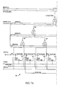
- an exemplary communications system 1 is illustrated in block form.
- This exemplary communications system 1 is a TDM communications system.
- the exemplary system 1 is comprised of three transceiver pairs, i.e., CFP1/CPP1, CFP2/CPP2, and CFP3/CPP3.
- Each transceiver pair includes a cordless fixed part 2, 4, 6 and a cordless portable part 8,10,12, respectively.
- the transceiver pairs each do not have any electrical cord extending between the related cordless fixed parts 2, 4, 6 and cordless portable parts 8, 10, 12.
- the cordless fixed parts 2, 4, 6 and their respective cordless portable parts 8, 10, 12 instead communicate by radio waves, i.e. TDM1, TDM2, TSM3.
- Radio wave signals between transceiver pairs operate in a time division multiplexed manner in which transmit signals and receive signals share a common communication channel by using different time intervals for the transmission of the intelligence of each signal.
- This exemplary communications system is like that of the typical cordless telephony systems now employed.
- the cordless fixed parts 2, 4, 6 are base units and the cordless portable parts 8, 10, 12 are handset units.
- interference area 14 for the cordless fixed parts 2, 4, 6 is illustrated as a box enclosing the cordless fixed parts 2,4,6.
- transmission signals of each of the cordless fixed parts 2,4,6 can reach the other cordless fixed parts 2,4,6.
- this noise and interference can occur when the transmitters of the cordless fixed parts 2, 4, 6 transmit at different times. This is because the transmitters of the cordless fixed parts 2,4,6 generate RF energy at a high level relative to the low level at which the receivers of the cordless fixed parts 2, 4, 6 detect RF energy.
- each cordless fixed part 2,4,6 transmits during the same time interval and receives during the same time interval.
- the transmissions and receptions of the cordless fixed parts 2, 4, 6 are synchronized. As previously described, this synchronization is desirable to eliminate the problems of noise and interference between cordless fixed parts 2, 4, 6 due to the relatively different transmit and receive RF energy levels for the system 1.
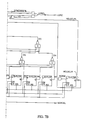
- FIG. 3 certain other possible transmit and receive signal timing for the three transceiver pairs of the TDM communications system of FIG. 1 is shown.
- the signals along the time line for each cordless fixed part 2, 4, 6 differs from the time lines for the other cordless fixed parts 2,4,6.
- the transmissions and receptions of the cordless fixed parts 2,4,6 are not synchronized.
- This asynchrony results in noise and interference between the cordless fixed parts 2,4,6 due to the relatively different transmit and receive RF energy levels being simultaneously felt within the interference area 14.
- This asynchronous arrangement is not desirable because mechanisms for rejecting unintended signals must be incorporated in the cordless fixed parts 2,4,6. Otherwise, the system 1 is hampered by noise and interference.
- the preferred embodiment of the present invention achieves synchronous timing of transmitters and, therefore, eliminates the problems of asynchronous timing in these systems 1.
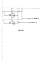
- a single transceiver pair 11 operation of a single transceiver pair 11 is illustrated.
- one transceiver, a first transceiver 12, of the transceiver pair 11 transmits a signal and the other transceiver, a second transceiver 13, of the transceiver pair 11 receives the signal, for example, a radio frequency wave signal.
- the signal is transmitted according to the timing of the first transceiver 12 counter.
- the signal does not follow the exact timing of the first transceiver 12 counter, however, due to the phenomenon of transmit modem delay, illustrated by box 14.
- the signal, delayed by the transmit modem delay 14, then proceeds to an antenna 16 and then on to the second transceiver 13.
- the signal is also affected by a delay effect, receive modem delay, illustrated by box 15. Only after the signal is delayed by the receive modem delay 15 does the second transceiver 13 detect the signal according to the timing of the second transceiver counter.
- modem delay (or “modidly”) shall mean the sum of the transmit modem delay 14 and the receive modem delay 15 for a particular transceiver pair.
- the concept of the embodiment of the present invention is illustrated and can be discussed. If the modem delay for a particular transceiver pair is known and either the transmit modem delay or the receive modem delay is known, the unknown receive modem delay or transmit modem delay, as the case may be, may be determined by simple arithmetic.
- This principle forms the basis for the present invention that by setting the receive timing of multiple transceiver pairs ofaTDM communication system in synchrony, the transceiver pairs are also synchronized if transmit timers are pushed ahead of receive timers, according to transceiver design, by some set time value. By achieving such synchrony in such a communications system, the advantages previously discussed are realized.
- the transmit counter of each individual transceiver pair is pushed ahead in time of the receive counter by a set interval.
- the modem delay for such transceiver pair is specific for the pair.
- the user had to determine the modem delay (or each individual transceiver pair included a mechanism for making that determination) and program in the particular modem delay. That practice achieved a desired timing delay between receive signals and transmit signals for each transceiver pair, however, it did not synchronize timing for multiple transceiver pairs of a TDM communications system. Each pair nevertheless operated according to its own particular timing.
- FIG. 5 three example cases A,B,C of the principles of the preferred embodiment of the invention are illustrated.
- the cases are based on several assumptions.
- One assumption is that a known 500Hz signal is available to all transceiver pairs in a TDM communications system as a benchmark for synchronizing transmit and receive signals of the multiple transceiver pairs.
- Another assumption is that there are 61 ⁇ 2 bits between the signals, which bits may be varied, either increased or decreased, in order to synchronize the signals of the multiple transceiver pairs.
- One other assumption is that the modem delay for each transceiver pair and either the receive modem delay (in the case of the preferred embodiment) for each or the transmit modem delay for each are known.
- each of the cases A,B,C may be described.
- T xmodd transmit modem delay
- R xmodd receive modem delay
- the actual bits transmitted and the actual bits received are the same as the bits in the RF, that is 61 ⁇ 2 bits based on the particular assumptions. This case is hypothetical, though, because in the real world the bits transmitted and the bits received are each different than the bits in the RF because there will be some modem delay.
- T xmodd is 2 and R xmodd is 0, giving a modem delay (modidly) of 2.
- the transmit signal In order to synchronize the transmit and receive signals of this case with the 500 Hz benchmark signal, the transmit signal must be pushed up by 2 bits, as illustrated. When pushed up, there are only 4 % bits between transmit and receive, rather than 6% bits, so the transmit is coming 2 bits earlier than was the situation in case A. In case C, T xmodd is 0 and R xmodd is 3, giving a total modem delay (modidly) of 3. With respect to the receiver, then, the transmitter must be pushed ahead by 3 bit times.
- This case C illustrates the present invention operation scenario that by adjusting the timing of the receiver, the transmitter timing is adjusted.
- the transmit timers of the respective transceiver pairs will be synchronized.
- FIG. 6 an integrated circuit 20 that achieves timer adjustment according to the principles of the present invention (in order, for example, to synchronize transmit signals of cordless fixed parts of a TDM communications system) is illustrated.
- the particular embodiment shown and described is a preferred embodiment which is preferably employed in TDM transceiver pairs conforming to the CT2 standard.
- This same embodiment, as well as all possible alternative embodiments, which may have application in other TDM communication systems or otherwise are included in the invention.
- the preferred embodiment of the integrated circuit 20 is suitable for application in a situation in which the transmitter timer of a transceiver pair is pushed ahead of the receiver timer by a particular value according to design of the pair. As previously discussed, this has been the practice in the prior technology.
- the preferred embodiment may be added to the circuitry of the transceiver pairs without varying that prior practice. This situation seems desirable since the operation of pushing up the transmit timer with respect to receive timer by modem delay is necessary, at least in the cordless portable part (CPP), and an objective in design of transceiver pairs for these systems has been to utilize the same transmit/receive circuitry in both CPP and cordless fixed part (CFP).
- This operation of pushing up the transmit timer is necessary in the CPP because the CPP is responsible for lining up the time division multiplexing in the air. So, the CPP is completely a slave to the CFP, i.e., the CFP transmits something and the CPP has to listen to it, figure out what time it was sent, and push the CPP's transmitter timer ahead so that they line up in the air.
- the preferred embodiment of the invention does not disturb the circuitry that pushed up the transmit timer.
- an input of the receive modem delay value is necessary.
- the user must give the preferred embodiment of the integrated circuit 20 this value by programming it into a register, RMBD48.
- the preferred embodiment of the integrated circuit 20 calculates the total modem delay.
- the preferred embodiment of the integrated circuit 20 adjusts the receiver timing (either delays or pushes up) based on the receive modem delay and total modem delay values in respect of a known synchronizing signal supplied to the circuit 20. Therefore, by so adjusting the receiver timing of each CFP of a TDM communications system, the preferred embodiment of the integrated circuit 20 causes the transmit timing of all the CFP's to be synchronized.
- the preferred embodiment of the integrated circuit 20 generally comprises a phase lock loop 22, 24, 26, 28, 20, 32, 34 in order to synchronize the internal clock timing of the transceiver containing the integrated circuit 20, which timing is based on the chip's crystal signal 102 synchronized with the benchmark signal 100, to the internal clock timing of all other transceivers of the communications system.
- This synchronization of crystal signal 102 and benchmark signal 100 is necessary because the crystal signal 102 and the benchmark signal 100 will have some tolerance, and those signals 102, 100 will be a bit different.
- the phase lock loop 22, 24, 26, 28, 30, 32, 34 serves to synchronize the signals 102, 100.
- the benchmark signal 100 is 500 Hz and the crystal signal is 9.216 mHz.
- the crystal signal 102 is divided down through a chain of dividers 28, 32, 34 to get, in the preferred embodiment, a 500 Hz compare signal 116.
- This compare signal 116 is compared with a synchronization port 22 accepting the benchmark signal 100 to determine which of the signals 100, 116 is ahead.
- An integrator 26 counts how far ahead the farther ahead of the signals 100, 116 is from the other signal.
- a first divider 28, preferably a nominally divide by nine divider, can adjust the crystal signal 102, as necessary, to bring it into conformity with the benchmark signal 100.
- the first divider28 preferably adjusts the crystal signal 102 by one clock per frame (therefore, either an eight divide or a ten divide will from time to time occur) to take a little longer or a little shorter to run through the cycle. In this manner, the signals 100, 102 are eventually synchronized.
- a second divider 32 preferably a divide by one hundred twenty eight divider, and a third divider, preferably a divide by sixteen divider, yield the compare signal 116.
- signals 110, 118, 120 may be taken from this chain of dividers 28, 32, 24. Signals 118 are 32 kHz; Signal 110 is 8 kHz, and signals 120 are 500 Hz in the preferred embodiment.
- Synchronization does not take much time because the integrator 26 has determined how far off the signals 100, 116 are to each other, and the first divider 28, therefore, knows how many adjustments must be made.
- the integrated circuit 20 has its own internal 500 Hz clock that is lined up with the benchmark signal 100.
- each transceiver pair need only account for its respective operational idiosyncracies by adjusting transmit and/or receive timers according to those idiosyncracies.
- receive timer adjustment by virtue of known values of total modem delay and either receive modem delay (as in the preferred embodiment) or transmit modem delay come into pay.
- the transmit timer has been set at a particular time ahead of the receive timer in transceiver pairs of these systems. The same principles of the present invention would apply, however, if a receive timing is fixed in relation to transmit timing.
- a particular receive modem delay value must be determined specifically for each transceiver pair of these systems, and that value must be programmed into the preferred integrated circuit 20. This is accomplished in the preferred embodiment by means of the RMBD 48 of the integrated circuit 20.
- the same principles of the present invention apply if it is desired to synchronize receiver timing and transmit modem delay is known.
- receive timer adjustment in accordance with the principles of the invention results in synchronized transmit timing for all transceiver pairs of a system.
- a format divider 36 block receives the crystal signal 102 and signals 122 from the first divider 28.
- the format divider 28 is a nominal divide by eight divider which tracks what the first divider 28 is doing and adjusts the crystal signal 102 by two clocks per frame (i.e., every time first divider 28 makes two adjustments, format divider 36 makes one adjustment).
- the signals from the format divider 36 then go through a regular clock generation inside the format clock 21, for example, via mux mechanisms 38 and divider blocks 40, 42, 46, to get a bit clock 124, for example, a 72 kHz bit clock in the preferred embodiment. That bit clock 124 is what clocks receive counter 52.
- the receive counter 52 in the preferred embodiment controls a variety of matters with respect to reception. For example, in the preferred embodiment, the receive counter 52 tells the circuit 20 when to receive and what bit to receive. The receive counter 52 in the preferred embodiment also tells the circuit 20 the status (i.e. where its at) in the receive cycle.
- the several boxes 54, 56, 58, 60, 62, 64 below the divide blocks 40, 42, 46 and receive counter 52 represent a typical modem delay adjustment.
- the modem delay adjustment includes a shift down block 62, modem delay blocks 58, 60, a backup block 56, and a comparator 54 leading on to a transmit counter 64.
- the modem delay adjustment portion of the circuit 20 has in the past, for example, pushed ahead the transmitter timing by some desired value in relation to the receive counter.
- the modem delay adjustment portion of the circuit 20 shown in FIG. 6 is a representation of how that adjustment may be performed.
- a receive modem delay adjustment box 50 significant to performing the receive timer adjustment in accordance with the principles of the invention can be understood.
- the objective of the box 50 is to control the receive counter 52 based on the internal clock signal (500 Hz in the preferred embodiment) and a programmed receive modem delay value.
- Signals 118 and 120 are indicative of the status (i.e, where its at) of divider chain 32, 34 at certain places in time.
- the box 50 accomplishes its objectives by picking off certain states of the whole counter chain, decoding them, determining an appropriate state value that will start up the receiver timer correctly to give the desired effect of transmit timer synchronization, and loading the receive counter 52 at the right time with the value in order to start the receive counter 52 to achieve desired transmit timing.
- FIGS. 7 and 8 details of the receive modem delay adjustment box 50 and RMBD 48, a register into which the receive mode delay is programmed, respectively, are given.
- These schematics show the preferred embodiment of the invention. Those skilled in the art will understand and appreciate what is illustrated by these schematics. Although these schematics show the preferred embodiment, alternative embodiments in accordance with the principles of the invention are possible, as those skilled in the art will appreciate.
- an integrated circuit for a cordless telephone handset and base unit for example, such as the integrated circuit disclosed in our copending applications 93305465.2 (TT0139), 93305458.7 (TT0140), 93305450.4 (TT0141), 93305457.9 (TT0142), 93305466.0 (TT0143), 93305459.5 (TT0144), 93305482.7 (TT0145), 93305454.6 (TT0146), 93305461.1 (TT0147), 93305456.1 (TT0148), 93305449.6 (TT0149) and 93305453.8 (TT0150).
- the integrated circuit can be synchronized to an external 500 Hz signal (slave) or to an internally generated 500 Hz signal (master, default), to meet the requirements of CT2 Annex N for CFP's.
- software has visibility of the open-drain SYNC I/O signal, allowing software contention and hand-off mechanisms, and the present invention may be programmed as a master or slave to the SYNC signal.
- the invention phase-locks to the incoming 500 Hz signal.
- the invention supports larger peak jitter input, as long as the 216 ppm long term drift requirement is observed.
- CFP transmission of bit B1 in Mux 1 starts at the antenna nominally 7 bit periods after the SYNC signal rises.
- the receive timing is adjusted, indirectly adjusting the transmit data timing to meet the 7 bit delay requirement.
- Programmability is provided to allow for various RF delays.
- the programmable delay in conjunction with the programmed modem delay register allows any total RF modem delay (transmit modem delay + receive modem delay) up to 7.75 bit (107 psec).
- the BSYNC register When using the present invention in this application, the BSYNC register must be programmed before MECTR1 [4] is set, and MECTR1 [4] (Fifo clock enable) must be set for the format section 21 (shown in FIG. 6) to function correctly.
- Control register definition for the present invention in this particular integrated circuit application is as follows:
- the present invention is a significant improvement in the art.
- the present invention is believed to be especially effective when configured and employed as described herein, however, those skilled in the art will readily recognize that numerous variations and substitutions may be made in the invention and its use and configuration to achieve substantially the same results as achieved by the embodiments and, in particular, the preferred embodiment expressly described herein. Each of those variations is intended to be included in the description herein and forms a part of the present invention.
- the foregoing detailed description is, thus, to be clearly understood as being given by way of illustration and example only, the spirit and scope of the present invention being limited solely by the appended claims.
Applications Claiming Priority (2)
| Application Number | Priority Date | Filing Date | Title |
|---|---|---|---|
| US19194094A | 1994-02-04 | 1994-02-04 | |
| US191940 | 1994-02-04 |
Publications (2)
| Publication Number | Publication Date |
|---|---|
| EP0666677A2 true EP0666677A2 (fr) | 1995-08-09 |
| EP0666677A3 EP0666677A3 (fr) | 1999-04-14 |
Family
ID=22707546
Family Applications (1)
| Application Number | Title | Priority Date | Filing Date |
|---|---|---|---|
| EP95300696A Withdrawn EP0666677A3 (fr) | 1994-02-04 | 1995-02-03 | Synchronisation des transmissions dans un système de télécommunication sans fil |
Country Status (3)
| Country | Link |
|---|---|
| US (1) | US5898685A (fr) |
| EP (1) | EP0666677A3 (fr) |
| JP (1) | JPH07321770A (fr) |
Cited By (4)
| Publication number | Priority date | Publication date | Assignee | Title |
|---|---|---|---|---|
| US4991672A (en) * | 1988-03-25 | 1991-02-12 | Orion-Yhtyma Oy Normet | Automatic control system for the transfer of the drive power between a tractor and a trailer |
| EP0813322A2 (fr) * | 1996-06-11 | 1997-12-17 | Vlsi Technology, Inc. | Générateur de synchronisation asynchrone |
| EP0887960A1 (fr) * | 1997-06-27 | 1998-12-30 | STMicroelectronics S.A. | Circuit d'émission-réception pour relier une station de base à une centrale de commande de station de base selon la norme DECT |
| US6028853A (en) * | 1996-06-07 | 2000-02-22 | Telefonaktiebolaget Lm Ericsson | Method and arrangement for radio communication |
Families Citing this family (8)
| Publication number | Priority date | Publication date | Assignee | Title |
|---|---|---|---|---|
| WO1998018216A2 (fr) * | 1996-10-24 | 1998-04-30 | Philips Electronics N.V. | Systeme de communication numerique sans fil et station radio sans fil |
| JP3076260B2 (ja) * | 1997-03-10 | 2000-08-14 | 松下電器産業株式会社 | 情報提供装置 |
| FR2760920B1 (fr) * | 1997-03-12 | 2000-08-04 | Sagem | Procede de transmission de donnees entre des moyens de traitement de donnees et un reseau de radiocommunication et module et terminal mobile pour la mise en oeuvre du procede |
| US6751232B1 (en) * | 1997-12-22 | 2004-06-15 | Nortel Networks Limited | Method and apparatus for communicating data between first and second pairs of transceivers communicating on a common communications link |
| US6643281B1 (en) * | 1998-03-05 | 2003-11-04 | At&T Wireless Services, Inc. | Synchronization preamble method for OFDM waveforms in a communications system |
| FI112567B (fi) * | 1998-10-23 | 2003-12-15 | Nokia Corp | Radiolinkkijärjestelmän terminaalien synkronointi |
| DE10305373B4 (de) * | 2003-02-10 | 2006-05-11 | Siemens Ag | Verfahren zur Synchronisation der Datenübertragung mit wenigstens einem ersten Funksystem und wenigstens einem weiteren Funksystem |
| US20060153745A1 (en) * | 2005-01-11 | 2006-07-13 | Applera Corporation | Fluid processing device for oligonucleotide synthesis and analysis |
Citations (5)
| Publication number | Priority date | Publication date | Assignee | Title |
|---|---|---|---|---|
| GB2110055A (en) * | 1981-10-26 | 1983-06-08 | Gen Electric Co Plc | Cordless telephone systems |
| EP0375361A2 (fr) * | 1988-12-20 | 1990-06-27 | AT&T WIRELESS COMMUNICATIONS PRODUCTS LTD. | Système et méthode de communications bidirectionnelles |
| EP0414409A2 (fr) * | 1989-08-23 | 1991-02-27 | Ferranti Creditphone Limited | Systèmes de téléphone sans fil |
| WO1991003136A1 (fr) * | 1989-08-18 | 1991-03-07 | Byps Communications Limited | Procede et station primaire de commande d'un systeme telephonique |
| WO1994005107A1 (fr) * | 1992-08-18 | 1994-03-03 | At & T Wireless Communications Products Ltd. | Procede d'etablissement d'une liaison de communication dans un systeme telephonique numerique sans fil |
Family Cites Families (6)
| Publication number | Priority date | Publication date | Assignee | Title |
|---|---|---|---|---|
| US4706244A (en) * | 1985-01-15 | 1987-11-10 | Rockwell International Corporation | Frequency multiplexed telephone system |
| US5347562A (en) * | 1989-08-18 | 1994-09-13 | Hutchinson Personal Communications Limited | Synchronizing groups of base stations in time division duplex communication systems |
| US5201061A (en) * | 1990-07-23 | 1993-04-06 | Motorola, Inc. | Method and apparatus for synchronizing simulcast systems |
| US5239672A (en) * | 1991-06-28 | 1993-08-24 | Motorola, Inc. | Synchronization method and apparatus for simulcast transmission system |
| US5257404A (en) * | 1991-10-04 | 1993-10-26 | Motorola, Inc. | Simulcast synchronization and equalization system and method therefor |
| US5285443A (en) * | 1992-08-25 | 1994-02-08 | Motorola, Inc. | Method and apparatus for synchronizing a time division duplexing communication system |
-
1995
- 1995-02-03 EP EP95300696A patent/EP0666677A3/fr not_active Withdrawn
- 1995-02-03 JP JP7017120A patent/JPH07321770A/ja not_active Withdrawn
-
1997
- 1997-08-01 US US08/914,015 patent/US5898685A/en not_active Expired - Lifetime
Patent Citations (5)
| Publication number | Priority date | Publication date | Assignee | Title |
|---|---|---|---|---|
| GB2110055A (en) * | 1981-10-26 | 1983-06-08 | Gen Electric Co Plc | Cordless telephone systems |
| EP0375361A2 (fr) * | 1988-12-20 | 1990-06-27 | AT&T WIRELESS COMMUNICATIONS PRODUCTS LTD. | Système et méthode de communications bidirectionnelles |
| WO1991003136A1 (fr) * | 1989-08-18 | 1991-03-07 | Byps Communications Limited | Procede et station primaire de commande d'un systeme telephonique |
| EP0414409A2 (fr) * | 1989-08-23 | 1991-02-27 | Ferranti Creditphone Limited | Systèmes de téléphone sans fil |
| WO1994005107A1 (fr) * | 1992-08-18 | 1994-03-03 | At & T Wireless Communications Products Ltd. | Procede d'etablissement d'une liaison de communication dans un systeme telephonique numerique sans fil |
Cited By (7)
| Publication number | Priority date | Publication date | Assignee | Title |
|---|---|---|---|---|
| US4991672A (en) * | 1988-03-25 | 1991-02-12 | Orion-Yhtyma Oy Normet | Automatic control system for the transfer of the drive power between a tractor and a trailer |
| US6028853A (en) * | 1996-06-07 | 2000-02-22 | Telefonaktiebolaget Lm Ericsson | Method and arrangement for radio communication |
| EP0813322A2 (fr) * | 1996-06-11 | 1997-12-17 | Vlsi Technology, Inc. | Générateur de synchronisation asynchrone |
| EP0813322A3 (fr) * | 1996-06-11 | 1999-11-24 | Vlsi Technology, Inc. | Générateur de synchronisation asynchrone |
| EP0887960A1 (fr) * | 1997-06-27 | 1998-12-30 | STMicroelectronics S.A. | Circuit d'émission-réception pour relier une station de base à une centrale de commande de station de base selon la norme DECT |
| FR2765427A1 (fr) * | 1997-06-27 | 1998-12-31 | Sgs Thomson Microelectronics | Circuit d'emission-reception pour relier une station de base a une centrale de commande de station de base selon la norme dect |
| US6278868B1 (en) | 1997-06-27 | 2001-08-21 | Sgs-Thomson Microelectronics S.A. | Transceiver circuit including a circuit for measuring the delay introduced by telephone lines |
Also Published As
| Publication number | Publication date |
|---|---|
| US5898685A (en) | 1999-04-27 |
| EP0666677A3 (fr) | 1999-04-14 |
| JPH07321770A (ja) | 1995-12-08 |
Similar Documents
| Publication | Publication Date | Title |
|---|---|---|
| CA2157727C (fr) | Methode et appareil pour etablir un environnement de communication synchrone | |
| US7929575B2 (en) | System for maintaining synchronization between multiple asynchronous communication links | |
| KR0173016B1 (ko) | 중첩형 디지탈 위상 동기 루프 회로 및 센터 비트 샘플링 방법 | |
| KR100228470B1 (ko) | 통신 시스템에서 패킷 정렬하는 방법 및 장치 | |
| KR100297894B1 (ko) | 비실시간 방식의 tdma 시스템의 동기화 | |
| CA2158115C (fr) | Methode et dispositif pour accroitre le rendement d'utilisation du spectre | |
| US6470006B1 (en) | Timing control of transmission time slot | |
| KR100556843B1 (ko) | 이동 통신 단말기의 업/다운 링크 동기화 장치 및 방법 | |
| US5898685A (en) | Burst synchronization of time division multiplexed transceiver pairs | |
| JP3694396B2 (ja) | 無線通信装置及び無線通信方法 | |
| CA2220022A1 (fr) | Processeur de signaux de reseau de communications a etalement du spectre | |
| US20030117995A1 (en) | Method, mobile radiotelephone system, and station for determining a timing advance for a connection between two stations | |
| US7801202B2 (en) | Synchronization | |
| JP4324328B2 (ja) | 移動無線システムにおけるデータ伝送方法、移動局および基地局 | |
| AU1239599A (en) | Base station synchronization method and cellular system | |
| JP2639840B2 (ja) | ディジタル移動通信方式 | |
| CN112788736A (zh) | 可降低时钟更新复杂度的多成员蓝牙装置中的副蓝牙电路 | |
| US6345067B1 (en) | Clock regenerating circuit in direct spread spectrum communication system | |
| KR20010020211A (ko) | 외부 네트워크로의 위상 연속 동기를 갖는 통신 장치 | |
| JPH06103853B2 (ja) | 同一周波数時分割送受信移動通信方式 | |
| JP2871644B2 (ja) | Phsコードレスホン | |
| JP3048930B2 (ja) | ディジタルコードレス電話装置 | |
| KR0154465B1 (ko) | 동기망에 있어서 프레임에 따른 타임슬롯의 윈도우제어장치 | |
| JP2000023266A (ja) | ディジタルコードレス電話装置の接続装置 | |
| JPH03235436A (ja) | 移動通信装置 |
Legal Events
| Date | Code | Title | Description |
|---|---|---|---|
| PUAI | Public reference made under article 153(3) epc to a published international application that has entered the european phase |
Free format text: ORIGINAL CODE: 0009012 |
|
| AK | Designated contracting states |
Kind code of ref document: A2 Designated state(s): AT BE DE DK ES FR GB GR IE IT LU NL PT SE |
|
| PUAL | Search report despatched |
Free format text: ORIGINAL CODE: 0009013 |
|
| AK | Designated contracting states |
Kind code of ref document: A3 Designated state(s): AT BE DE DK ES FR GB GR IE IT LU NL PT SE |
|
| STAA | Information on the status of an ep patent application or granted ep patent |
Free format text: STATUS: THE APPLICATION IS DEEMED TO BE WITHDRAWN |
|
| 18D | Application deemed to be withdrawn |
Effective date: 19991015 |