EP0664656A2 - Distributeur intermédiaire électronique et numérique pour systèmes de communication de messages et de données - Google Patents
Distributeur intermédiaire électronique et numérique pour systèmes de communication de messages et de données Download PDFInfo
- Publication number
- EP0664656A2 EP0664656A2 EP94117980A EP94117980A EP0664656A2 EP 0664656 A2 EP0664656 A2 EP 0664656A2 EP 94117980 A EP94117980 A EP 94117980A EP 94117980 A EP94117980 A EP 94117980A EP 0664656 A2 EP0664656 A2 EP 0664656A2
- Authority
- EP
- European Patent Office
- Prior art keywords
- status signal
- data
- line
- bit packets
- memory
- Prior art date
- Legal status (The legal status is an assumption and is not a legal conclusion. Google has not performed a legal analysis and makes no representation as to the accuracy of the status listed.)
- Withdrawn
Links
- 238000004891 communication Methods 0.000 title description 21
- 230000015654 memory Effects 0.000 claims abstract description 40
- 230000005540 biological transmission Effects 0.000 claims abstract description 12
- 230000011664 signaling Effects 0.000 claims description 24
- 238000000034 method Methods 0.000 claims description 4
- 238000006243 chemical reaction Methods 0.000 claims 1
- 238000012360 testing method Methods 0.000 description 9
- 238000012545 processing Methods 0.000 description 8
- 238000010586 diagram Methods 0.000 description 6
- 238000001514 detection method Methods 0.000 description 5
- 230000008901 benefit Effects 0.000 description 4
- 239000011159 matrix material Substances 0.000 description 4
- 230000001960 triggered effect Effects 0.000 description 4
- 230000006870 function Effects 0.000 description 3
- 230000003370 grooming effect Effects 0.000 description 3
- 230000010354 integration Effects 0.000 description 2
- 238000012935 Averaging Methods 0.000 description 1
- 230000003321 amplification Effects 0.000 description 1
- 230000008859 change Effects 0.000 description 1
- 230000008878 coupling Effects 0.000 description 1
- 238000010168 coupling process Methods 0.000 description 1
- 238000005859 coupling reaction Methods 0.000 description 1
- 238000011157 data evaluation Methods 0.000 description 1
- 239000000835 fiber Substances 0.000 description 1
- 230000007257 malfunction Effects 0.000 description 1
- 230000007246 mechanism Effects 0.000 description 1
- 238000012544 monitoring process Methods 0.000 description 1
- 238000003199 nucleic acid amplification method Methods 0.000 description 1
- 230000008520 organization Effects 0.000 description 1
- 238000012856 packing Methods 0.000 description 1
- 230000008569 process Effects 0.000 description 1
- 239000004065 semiconductor Substances 0.000 description 1
Images


Classifications
-
- H—ELECTRICITY
- H04—ELECTRIC COMMUNICATION TECHNIQUE
- H04Q—SELECTING
- H04Q11/00—Selecting arrangements for multiplex systems
- H04Q11/04—Selecting arrangements for multiplex systems for time-division multiplexing
Definitions
- the invention relates to a digital electronic intermediate distributor for message and data transmission systems and to a method for message and data transmission.
- Telephone systems transmit information from an exchange to the telephone subscribers.
- the Information contains the status of the subscriber loop, "free / busy", and voice or data signals that come from various subscribers or are transmitted to them.
- the communication lines generally run from the exchange to a distributor interface, which is also called an intermediate distributor.
- this intermediate distributor establishes an electrically conductive connection from the exchange to the subscriber.
- changes in the connection to the intermediate distributor lead to physical changes in the wiring in the device.
- it is relatively complex to make a change in the electrical connection between a subscriber and the switching center.
- U.S. Patent 4,520,234 discloses a cable switching system that uses a logic array and a switching matrix with a record of the current matrix state of the switching subsystem.
- the switching matrix module is formed by a large number of relays.
- U.S. Patent 4,539,564 discloses a central matrix made up of a plurality of semiconductor analog switches.
- U.S. Patent 4,525,605 also discloses a system that uses relays to access the telephone lines.
- US Patent 3,562,435 discloses a switching system with an automatic main distributor.
- the system contains a network control circuit for controlling a switching network with a relay which is installed between the telephone lines.
- an intermediate distributor for connecting voice circuits between input and output connections, such as a connection with a subscriber and a connection with a switching center.
- Each subscriber connection is connected to a line card or a subscriber interface module (SIM) arranged on a line of an intermediate distributor.
- SIM subscriber interface module
- NIM network interface module
- the line cards (hybrids) convert the analog signals into digital signals that are processed by the intermediate distributor.
- digital interface connections can be provided (preferably with four digital line cards) which establish a connection with a data communication line which transmits compressed digital data.
- the line cards are connected to an interface unit for a voice frequency time channel for coupling network voice frequency signals with subscriber voice frequency signals (and vice versa).
- the signaling time channel interface unit is also provided for connecting loop signaling data from network line cards to the subscriber line cards (and vice versa).
- the signaling time channel interface contains one or more memories with two connections (random access memory, RAM), which are controlled by a sequential counter. After all time channels have been loaded, the incoming signaling data is replaced by a value from a look-up table, which is then written as a new signal (encoded on the outgoing line) into an address table (data grooming). The microprocessor can also write the data directly to the outgoing address (no data grooming). The data leaves the look-up table and is saved in an address table before it reaches the outgoing line card.
- RAM random access memory
- a hardware interrupt circuit is added to the lookup tables to notify the microprocessor that an illegal data packet has been received from the lookup tables. Since the incoming data is signaling data (which represents the status of a line, such as the subscriber line), the hardware interrupt circuit provides a mechanism for detecting errors. The software can use this error detection scheme by loading the top two bits of a valid data address with ones and loading an invalid data address with a zero in each position. If the "zero" is loaded with the highest position, an interrupt is triggered at the high level. If the "zero" is loaded into the next higher position, an interrupt is triggered at the low level. The interrupt circuit can be disabled for any interconnect where the high level interrupt can be masked after an interrupt occurs to allow detection of a return to a normal interrupt state (for example, if a line card is removed and replaced) becomes).
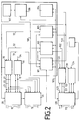
- FIG. 1 shows an intermediate distributor 1 for switching and monitoring the data exchange via individual network lines 15 and subscriber lines 12.
- Subscriber lines 12 are provided, each of which is connected to a subscriber 10 and a line card 20.
- the lines 12 are supplied and the loop current is monitored via the line card 20 (FIG. 2, 3).
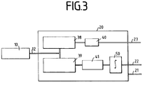
- 3 shows that the signal from subscriber 10 or switching center 2, if line card 20 is connected to network lines 15, is separated in line card 20.
- the data component usually the voice component, is passed from the data separator 38 to an analog / digital converter 40, the status signals separated in the status signal separator 39 are sent to an encoder / decoder 41.
- the encoder 41 converts the status signals into 8-bit packets or bytes at 8 kHz.
- Each status signal preferably has its own bit address; the data in this bit address indicate whether the status signal is present or not.
- the 8-bit packets or bytes can be passed to an integrator 50 for handling.
- the integrator 50 integrates or averages the status signals to remove noise spikes that would otherwise appear as erroneous message traffic.
- the integration or averaging can take place via a constantly moving window, or the status signals can be integrated or averaged at a lower rate.
- the integration eliminates misinterpretations of the line signals during later processing. Accordingly, through this processing the signals from the line card 20 are converted into event messages which are routed via channels 21, 22, 23 to a call processor, among other things, which has a well-functioning organization for each of the various lines.
- the 8-bit packets or bytes are routed from the line card 20 to a signaling TSI 102 (time channel interface).
- the signaling TSI 102 redirects the incoming status signals to the correct outgoing line with the correct time channel. This diversion takes place via assigned lines under the control of the switching center 2.
- Fig. 2 shows the system architecture with line cards 20 with thirty-two analog interface connections for processing the signals from the subscriber lines 12 and line cards 20 with thirty-two analog interface connections for processing the signals from the network lines 15 and the main control unit 104 and the connecting communication channels.
- the system is based on central processing, which is supported by control modules which are arranged at the common control point of the control unit 100. All secondary processors that are not arranged on the common control unit 100 are subordinate and are controlled by a plurality of internal communication buses, which are also shown in FIG. 2.
- the speech processing takes place in the time channel interface unit 103 for the voice frequency (VF).
- the processing is not intrusion and provides an interconnection of the language circles between the connections.
- a test pattern can be introduced and brought out from a speech PCM signal (pulse code modulation) for the purpose of a feedback test.
- the line circuit signaling is queried and brought to the signaling TSI 102 via a local processor 200 (FIGS. 5, 6).
- the status of the line circuit is monitored via NIM and SIM status registers (NIM means network interface modules, SIM means subscriber interface modules).
- NIM means network interface modules
- SIM means subscriber interface modules
- a bit pack scheme is provided which allows a local processor 200 to observe and send a call to the status registers in the signaling TSI 102.
- the SIM status register shows the status of the handset switch and the presence of the ring ground.
- the NIM status register shows loop detection forwards and backwards, presence of plug or ring earthing and the function "ringing".
- the communication bus 105 connects the main control unit 104, the digital group controller 130, the time channel interface unit 103, the signaling TSI unit 102 and the operator interface 106 to the Front panel 107.
- the system is preferably provided with full redundancy using a redundant module with a Bus structure executed, which is identical to that described above (two separate systems A and B).
- the group control module 30 for system A is identical to the group control module 33 for system B.
- system B which is identical to system A, is only shown up to connection 34.
- the communication bus 105 is very time-critical and is the main communication in the common control unit 100.
- This bus 105 is designed as an Ethernet network in a hub configuration.
- This bus 105 is duplicated for the A and B systems of the common control unit 100.
- Ethernet can be used as a "logical pipe", as a datagram or broadcast mode bus.
- the "digital bank" controls 130 in the DS1 bank are preferably accessible via the communication bus 105.
- test and configuration modules 101 transmit and receive non-real-time information from the line cards 20.
- the C and T connection interface (configuration and testing) is a 2 Mb / s control interface which is provided for each line card 20.
- the C and T interfaces are routed to the group control module 30 and again distributed over seven individual 2 Mb / s interfaces. These seven channels are distributed over the line cards 20.
- the C and T channels 21, 31 are used to write configuration information (control register A) to the individual line cards 20 (hybrids).
- the C and T channels 21, 31 are located where the transmission and reception filter is controlled for amplification and attenuation with respect to the encoder 41. This is also where the CODEC operating modes "normal”, "digital loopback", “analog loopback” and "no supply" are specified.
- the signal channel 32 is routed to the line card 20.
- the channel 32 is demultiplexed at the group controller 30 and again distributed as seven individual 2 Mb channels 22, one for each line card 20.
- the signal channel reading function supplies the main control unit 104 with signature information via the line cards 20, Display of a blown fuse and display group control 30 A or B active.
- the system according to the invention preferably supports 18 line compartments, 4032 connections.
- the maximum requirement is for a fully configured interconnection, where 2016 network interface modules and 2016 subscriber interface modules are supported.
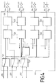
- FIG. 4 shows a quadruple DS1 module 120
- DS1 module 120 is a digital line card with 32 digital connections that are connected to digital lines 112.
- the digital lines 112 carry digitally compressed data signals at a DS1 rate (1.55 Mb / s).
- the digital module 120 has four connections 124 for each of the DS1 lines 1 to 4.
- Each connection 124 is connected to a combiner 126 via a data transmission buffer 125.
- the combiner 126 combines the outgoing speech frequency and signaling data from the intermediate distributor 1 and separates the incoming speech frequency and signaling data for input into the intermediate distributor 1.
- the communication signals can also be separated or combined in the combiner 126.
- the speech frequency signals are routed from the speech frequency selection unit 127 via the PCM-VF bus 123.
- the communication signals are routed through the communication selector 127 (to select system A or B, whichever of them is active) and via the communication bus 105.
- the signaling data are sent out via the signal bus 122.
- a configuration and test bus 131 (FIG. 2) is provided in the described type of configuration and test bus 121.
- the signal selection unit 129 and the speech frequency selection unit 128 select either system A or system B, whichever is active.
- FIG. 5 shows the digital group controller 130, which routes the signals to the line cards 20 and receives signals from the digital line cards 20, and the Forwards signals to or from the TSI unit 103 or the signal TSI unit 102.
- the signals from (to) the line cards 20 can be multiplexed (demultiplexed) in the unit 134 for forwarding via the signal bus 132 to the signal TSI unit 102.
- the voice frequency signals are transmitted via the bus 133 with the VF-TSI Unit 103 and connected to a configuration and test bus 131, which connects the digital group controller 130 to the test and configuration module 101.
- the outputs 135 of the unit 134 lead to the connections 124 of the quadruple DS1 module 120 (FIG. 4).
- FIG. 6 shows the structure of the signal TSI unit 102.
- the TSI unit 102 is a signaling time channel interface with full access, in which signals are routed from the network lines 15 and also from the subscriber lines 12 into the TSI unit 102 .
- the signal data for the network lines 15 as well as for the subscriber lines 12 are output by the TSI unit 102. This enables flexibility, including the possibility of connecting network line 15 to network line 15.
- the TSI unit 102 contains a microprocessor 200.
- the microprocessor 200 is connected to the exchange 2 via an assigned line (such as an assigned time channel).
- the exchange 2 then controls the microprocessor 200 via a software network manager to determine the time channels for the signaling data and other data (voice frequency data).
- the 8-bit packets or bytes received by the line cards 20 can be treated in a bit-pack process, with status changes in the various lines being detected and communicated to the switching center 2 and the subscriber 10.
- the signaling data from the line cards 20 reach the TSI unit 102 via the 8 Mb / s bus 32, as described above and shown in FIG.
- the data is demultiplexed to a data rate of 2 Mb / s and then transferred to a serial / parallel converter.
- the data leave the serial / parallel converter as 8 bit wide packets with a 16 MHz rate.
- the data is then loaded sequentially into both memories 202, 204 via a sequential counter 205.
- the lower path shown in Fig. 6 is used by the event detection software.
- the two ports of memory 204 are bank switched and the data is loaded in bit packets into another two ports of memory 204 for reading by microprocessor 200.
- the microprocessor 200 for data evaluation and data determination has an address output 201 and a data input 203 to the memory 204 and an address output 207 and a data output 209 to the connection memory 206.
- the bit packets are placed in memory locations where a bit pack device reads the least significant bit and then the next least significant bit, etc. Bit packing is performed on all bits and is banked when all 2048 time channels are loaded are.
- the microprocessor 200 can then be used for event detection with software that can output new signaling data for the outgoing line card via the connection memory 206 and the lookup tables 208.
- the microprocessor 200 can be used in a more limited manner, or a comparison can be carried out on the basis of the output of the software system explained above, the data being output via a further time channel exchange, as in FIG following is described.
- the data coming in via channel 32 (network signaling data and subscriber signaling data) can be routed to memory 202 via the upper path shown in FIG. 6.
- Memory 202 preferably has two banks that allow writing and reading without problems.
- the microprocessor 200 (under the control of the exchange 2) provides time channels, the address of the data being stored in the memory 202 in the connection memory 206 in accordance with the established time channels.
- a sequential counter 210 sequentially increments the link memory 206, whereby link data is read from the memory 202 in time according to the link plan address. This data then becomes part of an address along with higher bits from link memory 206.
- connection data and the higher bits can then become a code of the outgoing network or subscriber line card (Data grooming) can be changed if necessary.
- Data grooming can be changed if necessary.
- the new data correspond to signal data for an outgoing line card 20, and the data read out from the connection memory 206 correspond to the data for an incoming line card 20.
- memory 204 receives data based on the address of line card 20.
- Memory 204 preferably has two banks, one bank being written and the other bank used to avoid conflicts.
- the data is written to one side (left) of memory 204 and read at the same location in memory 204 in a different bank (such as data at ADD 0002) in microprocessor 200.
- the microprocessor 200 can be used to evaluate and update the data or to force signal data when a problem is detected.
- the microprocessor 200 writes new data into an address position of the connection memory 206.
- the address position is determined by the exchange 2 and provides the time channel for the outgoing data. For example, data from ADD 0002 are evaluated and new data are written into ADD 0128 of the connection memory 206, which is currently an address. represents a corresponding data code to be sent.
- the sequential counter 210 sequentially reads data from the connection memory 206, which form an address for the following time channels. Then lookup table 208 is used, reading the data from incoming memory 202 based on its placement in link memory 206 (one address in time). The data then becomes part of the address along with the higher bits from link memory 206 for lookup table 208 with the output data or new data 212 in that selected address position. The new data 212 is then output to a parallel / serial converter, the data leaving the lookup tables 208 as an 8 bit packet and converted to serial data and then preferably multiplexed to a higher rate (e.g. 8 Mb / s) with which they are routed via bus 32 or bus 132 to a line card 20 or 120.
- a higher rate e.g. 8 Mb / s
- Processing the data for the time channel exchange as explained above provides several advantages.
- An important advantage of the exchange from lookup tables is that the microprocessor is freed up for other tasks.
- a hardware interrupt circuit can be added to the Lookup tables are used to inform the microprocessor when an illegal data packet has been received from the lookup tables. Since the look-up tables have the necessary bit packets with regard to the various signaling data, an error can be detected immediately. Since the top two bits of the lookup data are not sent to the outgoing address, this can be used to indicate a valid data address. The software can then take advantage of this possibility by loading the upper two bits of a valid data address with "one" and invalid data addresses with "zero" at each position.
- an interrupt can be triggered at the high level. If the "zero" is loaded into the next highest position, an interrupt can be triggered at the low level. Flexibility can be added to enable and disable the interrupt circuit for each interconnect. The high level interrupt can be masked after an interrupt has occurred to allow detection of a return to the normal interrupt (for example, if a line card has been removed and replaced). While particular embodiments have been shown and described in more detail to illustrate the application of the principles according to the present invention, it is obvious that the invention can be carried out in other ways without deviating from such principles.
Landscapes
- Engineering & Computer Science (AREA)
- Computer Networks & Wireless Communication (AREA)
- Use Of Switch Circuits For Exchanges And Methods Of Control Of Multiplex Exchanges (AREA)
- Sub-Exchange Stations And Push- Button Telephones (AREA)
Applications Claiming Priority (2)
| Application Number | Priority Date | Filing Date | Title |
|---|---|---|---|
| US172557 | 1988-03-24 | ||
| US08/172,557 US5430717A (en) | 1993-12-23 | 1993-12-23 | Digital electronic loop crossconnect and carrier system |
Publications (1)
| Publication Number | Publication Date |
|---|---|
| EP0664656A2 true EP0664656A2 (fr) | 1995-07-26 |
Family
ID=22628204
Family Applications (1)
| Application Number | Title | Priority Date | Filing Date |
|---|---|---|---|
| EP94117980A Withdrawn EP0664656A2 (fr) | 1993-12-23 | 1994-11-15 | Distributeur intermédiaire électronique et numérique pour systèmes de communication de messages et de données |
Country Status (7)
| Country | Link |
|---|---|
| US (1) | US5430717A (fr) |
| EP (1) | EP0664656A2 (fr) |
| JP (1) | JPH07212878A (fr) |
| AU (1) | AU7895294A (fr) |
| BR (1) | BR9405225A (fr) |
| DE (1) | DE4411479A1 (fr) |
| RU (1) | RU94044349A (fr) |
Families Citing this family (56)
| Publication number | Priority date | Publication date | Assignee | Title |
|---|---|---|---|---|
| US5748627A (en) * | 1994-06-10 | 1998-05-05 | Harris Corporation | Integrated network switch with flexible serial data packet transfer system |
| US6223054B1 (en) | 1997-02-26 | 2001-04-24 | Lightsource Telecom, Llc | Wireless local loop system utilizing independent central offices located in new residential and commercial developments |
| US6363080B1 (en) | 1997-02-26 | 2002-03-26 | Lightsource Telecom Llc | Method and apparatus for bypassing a local exchange carrier using analog in-band signaling |
| US5991310A (en) * | 1997-02-26 | 1999-11-23 | Dynamic Telecom Enginering, L.L.C. | Method and apparatus for bypassing a local exchange carrier to permit an independent central office to provide local calling services |
| US5970130A (en) * | 1997-02-26 | 1999-10-19 | Dynamic Telcom Engineering, L.L.C. | Independent central office which provides local and long distance calling services to new residential and commercial developments |
| US6122758A (en) * | 1997-05-13 | 2000-09-19 | Micron Electronics, Inc. | System for mapping environmental resources to memory for program access |
| US6189109B1 (en) | 1997-05-13 | 2001-02-13 | Micron Electronics, Inc. | Method of remote access and control of environmental conditions |
| US6192434B1 (en) | 1997-05-13 | 2001-02-20 | Micron Electronics, Inc | System for hot swapping a programmable adapter by using a programmable processor to selectively disabling and enabling power thereto upon receiving respective control signals |
| US6163853A (en) | 1997-05-13 | 2000-12-19 | Micron Electronics, Inc. | Method for communicating a software-generated pulse waveform between two servers in a network |
| US6170028B1 (en) | 1997-05-13 | 2001-01-02 | Micron Electronics, Inc. | Method for hot swapping a programmable network adapter by using a programmable processor to selectively disabling and enabling power thereto upon receiving respective control signals |
| US6499073B1 (en) | 1997-05-13 | 2002-12-24 | Micron Electronics, Inc. | System using programmable processor for selectively enabling or disabling power to adapter in response to respective request signals |
| US6219734B1 (en) | 1997-05-13 | 2001-04-17 | Micron Electronics, Inc. | Method for the hot add of a mass storage adapter on a system including a statically loaded adapter driver |
| US6243838B1 (en) | 1997-05-13 | 2001-06-05 | Micron Electronics, Inc. | Method for automatically reporting a system failure in a server |
| US6330690B1 (en) | 1997-05-13 | 2001-12-11 | Micron Electronics, Inc. | Method of resetting a server |
| US6304929B1 (en) | 1997-05-13 | 2001-10-16 | Micron Electronics, Inc. | Method for hot swapping a programmable adapter by using a programmable processor to selectively disabling and enabling power thereto upon receiving respective control signals |
| US6363497B1 (en) | 1997-05-13 | 2002-03-26 | Micron Technology, Inc. | System for clustering software applications |
| US6249828B1 (en) * | 1997-05-13 | 2001-06-19 | Micron Electronics, Inc. | Method for the hot swap of a mass storage adapter on a system including a statically loaded adapter driver |
| US6195717B1 (en) | 1997-05-13 | 2001-02-27 | Micron Electronics, Inc. | Method of expanding bus loading capacity |
| US6282673B1 (en) | 1997-05-13 | 2001-08-28 | Micron Technology, Inc. | Method of recording information system events |
| US6173346B1 (en) | 1997-05-13 | 2001-01-09 | Micron Electronics, Inc. | Method for hot swapping a programmable storage adapter using a programmable processor for selectively enabling or disabling power to adapter slot in response to respective request signals |
| US6170067B1 (en) | 1997-05-13 | 2001-01-02 | Micron Technology, Inc. | System for automatically reporting a system failure in a server |
| US6243773B1 (en) | 1997-05-13 | 2001-06-05 | Micron Electronics, Inc. | Configuration management system for hot adding and hot replacing devices |
| US6247080B1 (en) | 1997-05-13 | 2001-06-12 | Micron Electronics, Inc. | Method for the hot add of devices |
| US6249885B1 (en) | 1997-05-13 | 2001-06-19 | Karl S. Johnson | Method for managing environmental conditions of a distributed processor system |
| US6269417B1 (en) | 1997-05-13 | 2001-07-31 | Micron Technology, Inc. | Method for determining and displaying the physical slot number of an expansion bus device |
| US6292905B1 (en) | 1997-05-13 | 2001-09-18 | Micron Technology, Inc. | Method for providing a fault tolerant network using distributed server processes to remap clustered network resources to other servers during server failure |
| US6269412B1 (en) | 1997-05-13 | 2001-07-31 | Micron Technology, Inc. | Apparatus for recording information system events |
| US6249834B1 (en) | 1997-05-13 | 2001-06-19 | Micron Technology, Inc. | System for expanding PCI bus loading capacity |
| US6247079B1 (en) * | 1997-05-13 | 2001-06-12 | Micron Electronics, Inc | Apparatus for computer implemented hot-swap and hot-add |
| US6202111B1 (en) | 1997-05-13 | 2001-03-13 | Micron Electronics, Inc. | Method for the hot add of a network adapter on a system including a statically loaded adapter driver |
| US6253334B1 (en) | 1997-05-13 | 2001-06-26 | Micron Electronics, Inc. | Three bus server architecture with a legacy PCI bus and mirrored I/O PCI buses |
| US6134668A (en) * | 1997-05-13 | 2000-10-17 | Micron Electronics, Inc. | Method of selective independent powering of portion of computer system through remote interface from remote interface power supply |
| US6418492B1 (en) | 1997-05-13 | 2002-07-09 | Micron Electronics | Method for computer implemented hot-swap and hot-add |
| US6202160B1 (en) | 1997-05-13 | 2001-03-13 | Micron Electronics, Inc. | System for independent powering of a computer system |
| US6338150B1 (en) | 1997-05-13 | 2002-01-08 | Micron Technology, Inc. | Diagnostic and managing distributed processor system |
| US6324608B1 (en) | 1997-05-13 | 2001-11-27 | Micron Electronics | Method for hot swapping of network components |
| US6182180B1 (en) | 1997-05-13 | 2001-01-30 | Micron Electronics, Inc. | Apparatus for interfacing buses |
| US5987554A (en) * | 1997-05-13 | 1999-11-16 | Micron Electronics, Inc. | Method of controlling the transfer of information across an interface between two buses |
| US6163849A (en) * | 1997-05-13 | 2000-12-19 | Micron Electronics, Inc. | Method of powering up or powering down a server to a maintenance state |
| US6145098A (en) | 1997-05-13 | 2000-11-07 | Micron Electronics, Inc. | System for displaying system status |
| US6179486B1 (en) | 1997-05-13 | 2001-01-30 | Micron Electronics, Inc. | Method for hot add of a mass storage adapter on a system including a dynamically loaded adapter driver |
| US6212585B1 (en) | 1997-10-01 | 2001-04-03 | Micron Electronics, Inc. | Method of automatically configuring a server after hot add of a device |
| US6199173B1 (en) | 1997-10-01 | 2001-03-06 | Micron Electronics, Inc. | Method for mapping environmental resources to memory for program access |
| US6175490B1 (en) | 1997-10-01 | 2001-01-16 | Micron Electronics, Inc. | Fault tolerant computer system |
| US6263387B1 (en) | 1997-10-01 | 2001-07-17 | Micron Electronics, Inc. | System for automatically configuring a server after hot add of a device |
| US6138179A (en) * | 1997-10-01 | 2000-10-24 | Micron Electronics, Inc. | System for automatically partitioning and formatting a primary hard disk for installing software in which selection of extended partition size is not related to size of hard disk |
| US6154835A (en) * | 1997-10-01 | 2000-11-28 | Micron Electronics, Inc. | Method for automatically configuring and formatting a computer system and installing software |
| CA2254811C (fr) * | 1997-12-04 | 2007-09-18 | Nippon Telegraph And Telephone Corporation | Reseau de communication a mode de transfert synchrone (stm) |
| US5989074A (en) * | 1997-12-18 | 1999-11-23 | The Whitaker Corporation | Wire pair disconnect module |
| US6205503B1 (en) | 1998-07-17 | 2001-03-20 | Mallikarjunan Mahalingam | Method for the hot swap and add of input/output platforms and devices |
| US6223234B1 (en) | 1998-07-17 | 2001-04-24 | Micron Electronics, Inc. | Apparatus for the hot swap and add of input/output platforms and devices |
| US6301246B1 (en) * | 1998-08-17 | 2001-10-09 | Siemens Information And Communication Networks, Inc. | Silent monitoring in a voice-over-data-network environment |
| US7162017B1 (en) | 2002-05-23 | 2007-01-09 | Verizon Laboratories Inc. | System and method for determining an optimal threshold for increasing telephone line capacity and for evaluating line management policies |
| KR100726573B1 (ko) * | 2004-09-22 | 2007-06-11 | 주식회사 케이티 | Dcs 서버를 이용하는 통신망 관리시스템에서 제어정보원격 감시시스템 및 이에따른 감시방법 |
| US7782017B2 (en) * | 2006-02-28 | 2010-08-24 | Linear Technology Corporation | Apparatus and method for producing signal conveying circuit status information |
| US9882613B2 (en) * | 2015-06-01 | 2018-01-30 | Corning Optical Communications Wireless Ltd | Determining actual loop gain in a distributed antenna system (DAS) |
Family Cites Families (7)
| Publication number | Priority date | Publication date | Assignee | Title |
|---|---|---|---|---|
| US3562435A (en) * | 1968-12-27 | 1971-02-09 | Bell Telephone Labor Inc | Switching system with automated main distributing frame |
| ZA786110B (en) * | 1977-11-07 | 1979-10-31 | Post Office | Improvements in or relating to the switching of digital signals |
| DE3107046A1 (de) * | 1981-02-25 | 1982-09-09 | Siemens AG, 1000 Berlin und 8000 München | Schaltungsanordnung zum verbinden von analog-signale abgebenden sendeeinrichtungen mit analog-signale aufnehmenden empfangseinrichtungen ueber eine zeitmultiplex-datenvermittlungsanlage |
| US4539564A (en) * | 1982-08-04 | 1985-09-03 | Smithson G Ronald | Electronically controlled interconnection system |
| US4525605A (en) * | 1982-12-08 | 1985-06-25 | Wiltron Company | System for accessing electrical circuits and relay switch thereof |
| US4520234A (en) * | 1983-04-11 | 1985-05-28 | Remote Switch Systems, Inc. | Remote cable switching system |
| US5268903A (en) * | 1991-10-02 | 1993-12-07 | Rockwell International Corporation | Multichannel telephonic switching network with different signaling formats and cross connect/PBX treatment selectable for each channel |
-
1993
- 1993-12-23 US US08/172,557 patent/US5430717A/en not_active Expired - Fee Related
-
1994
- 1994-03-29 DE DE4411479A patent/DE4411479A1/de not_active Withdrawn
- 1994-11-15 EP EP94117980A patent/EP0664656A2/fr not_active Withdrawn
- 1994-11-21 AU AU78952/94A patent/AU7895294A/en not_active Abandoned
- 1994-12-16 JP JP6313368A patent/JPH07212878A/ja active Pending
- 1994-12-22 BR BR9405225A patent/BR9405225A/pt not_active Application Discontinuation
- 1994-12-22 RU RU94044349/09A patent/RU94044349A/ru unknown
Also Published As
| Publication number | Publication date |
|---|---|
| AU7895294A (en) | 1995-06-29 |
| BR9405225A (pt) | 1995-08-01 |
| JPH07212878A (ja) | 1995-08-11 |
| RU94044349A (ru) | 1996-10-20 |
| DE4411479A1 (de) | 1995-07-13 |
| US5430717A (en) | 1995-07-04 |
Similar Documents
| Publication | Publication Date | Title |
|---|---|---|
| EP0664656A2 (fr) | Distributeur intermédiaire électronique et numérique pour systèmes de communication de messages et de données | |
| DE2903650C2 (de) | Schaltungsanordnung für eine PCM-Vermittlungsanlage | |
| CH662025A5 (de) | Digitale vermittlungsanlage. | |
| DE2723138C2 (de) | Prozessorgesteuertes Koppelfeld einer Fernmeldevermittlungsanlage | |
| EP0763953B1 (fr) | Procédé pour le chargement de software dans des systèmes de communication équipés de dispositif décentralisés et non-redondants | |
| DE2848255C2 (fr) | ||
| DE3921573C2 (de) | Digitale Kommunikationsvorrichtung | |
| DE69124217T2 (de) | Verteilte Telefonkonferenz-Kontrolleinrichtung | |
| EP0923835B1 (fr) | Procede de surveillance et de verification des raccordements d'un reseau rnis de telecommunication | |
| DE2838142C2 (de) | Rechnergesteuertes Fernmeldevermittlungssystem mit Zeitvielfach-Durchschaltung | |
| DE3331446C2 (fr) | ||
| DE4422805C1 (de) | Verfahren zum Laden von Software in Kommunikationssystemen mit nichtredundaten, dezentralen Einrichtungen | |
| EP0110464A1 (fr) | Standard privé | |
| DE19506961C1 (de) | Verfahren zum Anschluß von Access-Networks mit V5.2-Schnittstellen an Kommunikationssysteme mit nichtredundanten peripheren Einrichtungen | |
| CH656276A5 (de) | Verfahren und schaltungsanordnung zum uebertragen von datensignalen zwischen datenvermittlungseinrichtungen einer datenvermittlungsanlage. | |
| EP0006133B1 (fr) | Système de commutation à commande indirecte avec joncteurs à division temporelle, en particulier système de commutation téléphonique | |
| DE2808666C2 (de) | Dezentral gesteuerte Fernsprechvermittlungsanlage | |
| EP1097605A2 (fr) | Procede et circuit pour creer des liaisons de signaux de donnees | |
| DE69933377T2 (de) | Ressourcenschnittstelleneinheit für einen fernmeldevermittlungsknoten | |
| EP0477627B1 (fr) | Procédé pour connecter des terminaux de communication dans les réseaux de commutation à services integrés | |
| DE3212237C2 (de) | Schaltungsanordnung für zentralgesteuerte Fernmeldeanlagen, insbesondere Fernsprechnebenstellenanlagen, mit über Datenübertragungsleitungsbündel steuerbaren zentralen und dezentralen Einrichtungen (dezentrale Rückstelleinheiten) | |
| DE3932700C2 (de) | Verfahren zur Durchschalteprüfung eines Koppelnetzes | |
| EP0006134A1 (fr) | Système de commutation à commande indirecte avec joncteurs à division temporelle, en particulier système de commutation téléphonique | |
| DE3901433C2 (fr) | ||
| EP0553436B1 (fr) | Méthode pour tester le fonctionnement de liaisons de transmission de signaux de télécommunication |
Legal Events
| Date | Code | Title | Description |
|---|---|---|---|
| PUAI | Public reference made under article 153(3) epc to a published international application that has entered the european phase |
Free format text: ORIGINAL CODE: 0009012 |
|
| AK | Designated contracting states |
Kind code of ref document: A2 Designated state(s): AT BE CH DE DK ES FR GB GR IE IT LI LU MC NL PT SE |
|
| STAA | Information on the status of an ep patent application or granted ep patent |
Free format text: STATUS: THE APPLICATION HAS BEEN WITHDRAWN |
|
| 18W | Application withdrawn |
Withdrawal date: 19960930 |