EP0664613B1 - Verfahren und Vorrichtung zur Symmetrierung der Belastung parallelgeschalteter Leistungshalbleitermodule - Google Patents
Verfahren und Vorrichtung zur Symmetrierung der Belastung parallelgeschalteter Leistungshalbleitermodule Download PDFInfo
- Publication number
- EP0664613B1 EP0664613B1 EP94810725A EP94810725A EP0664613B1 EP 0664613 B1 EP0664613 B1 EP 0664613B1 EP 94810725 A EP94810725 A EP 94810725A EP 94810725 A EP94810725 A EP 94810725A EP 0664613 B1 EP0664613 B1 EP 0664613B1
- Authority
- EP
- European Patent Office
- Prior art keywords
- current
- difference
- control signal
- load
- switch
- Prior art date
- Legal status (The legal status is an assumption and is not a legal conclusion. Google has not performed a legal analysis and makes no representation as to the accuracy of the status listed.)
- Expired - Lifetime
Links
Images



Classifications
-
- H—ELECTRICITY
- H03—ELECTRONIC CIRCUITRY
- H03K—PULSE TECHNIQUE
- H03K17/00—Electronic switching or gating, i.e. not by contact-making and –breaking
- H03K17/12—Modifications for increasing the maximum permissible switched current
- H03K17/127—Modifications for increasing the maximum permissible switched current in composite switches
-
- H—ELECTRICITY
- H03—ELECTRONIC CIRCUITRY
- H03K—PULSE TECHNIQUE
- H03K17/00—Electronic switching or gating, i.e. not by contact-making and –breaking
- H03K17/08—Modifications for protecting switching circuit against overcurrent or overvoltage
- H03K17/081—Modifications for protecting switching circuit against overcurrent or overvoltage without feedback from the output circuit to the control circuit
- H03K17/0812—Modifications for protecting switching circuit against overcurrent or overvoltage without feedback from the output circuit to the control circuit by measures taken in the control circuit
- H03K17/08128—Modifications for protecting switching circuit against overcurrent or overvoltage without feedback from the output circuit to the control circuit by measures taken in the control circuit in composite switches
-
- H—ELECTRICITY
- H03—ELECTRONIC CIRCUITRY
- H03K—PULSE TECHNIQUE
- H03K17/00—Electronic switching or gating, i.e. not by contact-making and –breaking
- H03K17/08—Modifications for protecting switching circuit against overcurrent or overvoltage
- H03K17/082—Modifications for protecting switching circuit against overcurrent or overvoltage by feedback from the output to the control circuit
- H03K17/0828—Modifications for protecting switching circuit against overcurrent or overvoltage by feedback from the output to the control circuit in composite switches
-
- H—ELECTRICITY
- H03—ELECTRONIC CIRCUITRY
- H03K—PULSE TECHNIQUE
- H03K17/00—Electronic switching or gating, i.e. not by contact-making and –breaking
- H03K17/12—Modifications for increasing the maximum permissible switched current
-
- H—ELECTRICITY
- H03—ELECTRONIC CIRCUITRY
- H03K—PULSE TECHNIQUE
- H03K17/00—Electronic switching or gating, i.e. not by contact-making and –breaking
- H03K17/16—Modifications for eliminating interference voltages or currents
- H03K17/161—Modifications for eliminating interference voltages or currents in field-effect transistor switches
- H03K17/165—Modifications for eliminating interference voltages or currents in field-effect transistor switches by feedback from the output circuit to the control circuit
- H03K17/166—Soft switching
- H03K17/167—Soft switching using parallel switching arrangements
Definitions
- the invention relates to the field of power electronics.
- it relates to a method and an apparatus for balancing the Load distribution of at least two switch modules connected in parallel according to the preamble of claim 1 or 7.
- the switch modules include at least one Power semiconductor switch with a gate connection through a pulse Control signal can be switched on or off repeatedly at any switching times and thus either in a current-conducting or a current-blocking state is.
- the method includes measuring an actual load value of each Switch module, forming a difference between a load setpoint and the actual load value and a determination and setting of switch-on and Switch-off times of the control signal for each power semiconductor switch based on the difference between the target load value and the actual load value, that in the event of a negative difference, the switch module at the next switching operation is switched on later and in the case of a positive difference that Switch module is switched on earlier during the next switching process.
- the European patent application EP 0 511 344 discloses a parallel connection several inverters. To even load - in this case Current distribution - to get between the converter branches, the outputs of the converter branches interconnected via connection chokes. Is the If the current in a converter branch is too large, regulation will reduce the Switch of the corresponding converter branch opened earlier, so that between a compensation path is created for the converter branches and the currents due to the Connection chokes can be evenly distributed across all converter branches. While closing the switch can be moved accordingly.
- connection chokes increases and thus the dynamics of the arrangement is reduced.
- volume of the connection chokes increases with it falling clock frequency, which leads to very large connection chokes, especially at low frequencies leads.
- the object of the present invention is therefore a method and a device to symmetrize the load distribution of at least two Train switch modules connected in parallel, which distribute the load evenly without additional connection chokes and in particular also taking into account parameter differences and temperature.
- the switch-on and switch-off times each switch module according to the difference between the load setpoint and actual load value determined and set.
- the current flow of the power semiconductor switch is via the gate connection by means of a pulse Control signal controllable.
- the level of the control signal for each switch module set such that in the event of a negative difference between a Load setpoint and an actual load value the level of the control signal is reduced and in the case of a positive difference the level of the control signal is enlarged.
- a first embodiment uses the actual load value a temperature Ts of the switches.
- a setpoint serves a maximum temperature value specified from the outside Tmax. If the actual temperature value Ts is greater than the maximum value Tmax, the level of the control voltage is reduced. In this way, the load is achieved the modules are distributed as evenly as possible and the temperature of none of the modules the maximum allowed temperature exceeds.
- a second embodiment uses the actual load value an actual current value that flows through a module and is measured.
- a current setpoint is used as the setpoint used.
- the aim of this procedure is the total current to be distributed symmetrically across all modules.
- a particularly preferred embodiment of the current balancing method is characterized by that for a switching process during the switch-on or switch-off time the difference between the setpoint and actual value of the current formed by the module in time between two corresponding switching times the on or. Switch-off times for the next switching operation are calculated and the switches with control signals with the specific switch-on and switch-off times be charged. At the same time, the difference becomes again measured from the setpoint and actual value of the current etc. On this is achieved after a few switching operations a uniform current distribution in the modules, which Adaptive changes.
- the modules are switched on later using this procedure and / or turned off earlier if the difference of the setpoint and actual value of the current is negative or switched on earlier and switched off later if the difference is positive.
- the current cannot only be transient, i.e. during the Switching on or off, but also stationary, i.e. yogem the switches carry a current, are balanced. This stationary compensation is obtained by that the level of the control signal is adjusted.
- Either the mean value of the total current can be used as the current setpoint or an externally specified one is used become.
- a device for performing the method with the Temperature measurement includes a temperature measurement device for each module and a control unit.
- the control unit is the by means of a temperature comparator Difference between maximum temperature value and measured Actual value formed. This difference is used in one Compensating regulator determines the level of the control voltage and this is in a control signal shaper according to the height set in the compensation regulator.
- the device for performing the current balancing method is characterized in that for each module a current measuring device is provided which Measures current through the module. For each module there is also a control unit is provided in which the comparison between the current setpoint and actual value. moreover is in the control unit for each switch of the module a compensation regulator and a control signal shaper are provided. In the compensation controller, the difference becomes the Switch-on and switch-off times and the level of the control signals calculated, and in the control signal shaper Control signals based on the calculated switch-on and switch-off times or signal levels changed. With these control signals finally the switches of the modules are activated.
- the current setpoint for each module can either be through averaging or by specifying the actual current of a higher-level module that has a predetermined target current has to be formed.
- the advantage of the construction according to the invention is in particular in that the regulation for even load distribution no additional connection chokes needed and also on parameter differences of the wiring or of the semiconductor as well as the temperature.
- FIG. 1a shows a circuit for which the inventive Regulation with current measurement can be used. It is a phase of an inverter.
- the Converter consists of several power semiconductors connected in parallel or switch modules (1).
- the switch modules (1) in turn consist of power semiconductor switches (2) which e.g. as shown e.g. the Can form branches of a bridge circuit. In this Fall is between the switches of a module (1) Load connection (8) available.
- Each module (1) carries one Current (i1..n) to the total current (itot) at.
- the switches (2) of the modules (1) are triggered by control signal pulses (UGE) repeatedly switched on and off.
- the switch (2) of the Modules (1) are either on or off Status.
- the switches (2) are especially about IGBTs.
- the regulation according to the invention now tries to counteract this, by making sure that the total current (itot) is evenly distributed over the modules (1) and none of the switches (2) leaves its SOA.
- switch-on and switch-off times (ton, toff) of the control signal (UGE) can be set for each switch (2) that when switching on or off a uniformly distributed Current load is reached.
- level of the control voltage (UGE) for the conductive switches are set so that the Current load becomes the same.
- each switch module (1) is therefore for each input and Switch-off time (ton, toff) a difference between a current setpoint (isoll1..n) and the measured Current actual value (i1..n) formed. From this difference now in the time between two corresponding switching times the switch-on and switch-off times (ton, toff) destined for the next switching operation.
- the switches (2) the modules (1) are finally with control signals (UGE), which the previously determined switching times have applied. At the same time it is already again the difference between the current setpoint and the current actual value formed, etc. With time you get one even distribution of the currents (i1..n) to all modules (1).
- the Switch (2) of the modules (1) during the next switching process should be switched on or off sooner or later.
- the modules (1) are switched on later in particular, if the difference is negative, i.e. the actual current is greater than the target current is. Conversely, the modules (1) switched on earlier if the difference is positive, i.e. the actual current is smaller than the target current. It can also the switch-off time can also be influenced. If negative Difference, the modules are switched off earlier, if positive later.
- the current distribution to the modules (1) can be compensated for during the transient switching processes.
- FIG. 3a shows, different currents flow through the modules not only when switching, but also in the stationary, conductive state.
- the current through an IGBT or a related element can now be influenced by increasing or decreasing the level of the control voltage (UGE). In this way it is possible to obtain an equally distributed current distribution even in the steady state. This is achieved in particular by continuously forming a difference between the current setpoint (isolll..n) and the measured current actual value (i1..n). If the difference is negative, the level of the control signal is reduced, if it is positive it is increased.
- UGE control voltage
- the current setpoint for each module (1) can e.g. thereby be calculated that the total current (itot) of the parallel Module is measured and by the number the module (1) is shared. Likewise, the sum of the measured actual currents (i1..n) are formed and a Average value can be calculated.
- each module (1) has its own setpoint (isoll1..n) specifies, the control system is overdetermined, and the system may become unstable. Therefore there is another variant of the setpoint formation in giving a setpoint to a first module (isoll1) specifies the actual current for the other modules (i1) of the first module as setpoint (isoll2..n) used. In this way you also get one even distribution of the currents among the modules (1).
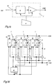
- FIGS. 1a-e A possible device for carrying out the method explained above is shown for a module (1) in FIGS. 1a-e .
- the module (1) comprises two switches (2), which are connected in series and, with their common node, form a load connection (8) of a bridge circuit.
- the switches (2) are closed or opened by control signals (UGE).
- the control signal (UGE) is pulse-shaped and is supplied by a control signal source, not shown.
- a control unit (3) is now provided for each module (1), which are the control signals given from the outside (USt) changed so that the desired current balancing is achieved.
- This actual current (i1..n) is now with a Target current (isoll1..n) compared.
- the target current (isoll1..n) can, as explained above, in different ways be formed.
- the comparison takes place in a difference generator (5).
- a downstream compensation regulator (6) are now based on the difference between target and actual value the required switch-on and switch-off times (ton, toff) or the level of the control signal (UGE) is calculated.
- Either one can be used to form the current setpoint Total current measuring device (9) with a downstream divider (11) (FIG. 1a) or an averager (10) ( Figure ld) may be provided.
- FIG. 1e Another variant, which is shown in FIG. 1e, is that a first module has a setpoint (isoll1) is specified from the outside and for the others Module the actual value (i1) of the first module as setpoint (isoll2..n) is used ( Figure 1e).
- FIGS. 4a-d and 5a-b show measurement results that were achieved with an experimental setup.
- the currents when switching on (FIGS. 4a, b), when switching off (FIGS. 4c, d) and when conducting (FIGS. 5a, b) were measured both with and without regulation according to the invention.
- the currents (i1..3) in the experiments with regulation (FIGS. 4b, 4d, 5b) are symmetrized much better than in the experiments without regulation according to the invention (FIGS. 4a, 4c, 5a).
- the regulation set out above can also be a regulation be superimposed on the thermal load. This is from special advantage, because of the effective junction temperature the switch can directly on a possible danger of destruction. So it is perfectly allowed that a switch may have a higher one Current runs as long as the junction temperature does not become too large, this does not harm the switch.
- FIG. 6 shows a possible implementation of such a combined current and temperature control: the actual value of the temperature Ts is measured directly on the switches (2) and compared in a temperature comparator (12) with a predetermined maximum value Tmax. Based on this comparison, the target current value (Isoll1..n) is now influenced in a second difference generator (15).
- the second difference generator (15) is connected upstream of the first (5) and is connected to the setpoint input (14) and the output of the temperature comparator (12). If the temperature Ts is higher than the maximum permitted Tmax, the target current value (isoll) is reduced. For example, an amount is subtracted that is proportional to the temperature difference found. In this way, it is effectively avoided that a switch is loaded with a current that results in an excessively high junction temperature and could therefore lead to the switch being destroyed.
- This higher-level temperature control can of course accordingly also for the other types of current target value determination be transmitted.
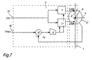
- FIG. 7 finally shows an exemplary embodiment of a device for carrying out the method with the temperature measurement.
- a control unit (3) is again provided for each module (1). Instead of a current setpoint input (14), a temperature maximum value input (18) is now provided.
- the temperature Ts of the switches (2) of a module (1) is measured in a temperature measuring device (17). This temperature Ts is then compared with the maximum value Tmax in a temperature comparator (12) - for example a difference former.
- the result of the comparison is fed to a compensation regulator (6), in which, if the difference between the actual temperature value Ts and the maximum value Tmax is negative, a reduction in the level of the control voltage (UGE) is calculated.
- a control signal shaper (7) is also provided for each switch (2), in which the control signal (Ust) present at the control signal input (13) is changed in accordance with the values calculated in the compensation controller (6).
- the invention provides an effective control method to symmetrize the load in parallel switched power semiconductor modules are available. With this method, the advantages in particular that no module is overloaded and the Modules used in their intended performance range can be without derating. This regulation will also ensures that the modules or their switches the safe operating area (SOA) both in terms of current and temperature loads do not leave.
- SOA safe operating area
Landscapes
- Power Conversion In General (AREA)
- Electronic Switches (AREA)
- Dc-Dc Converters (AREA)
- Container, Conveyance, Adherence, Positioning, Of Wafer (AREA)
- Control Of Multiple Motors (AREA)
- Supply And Distribution Of Alternating Current (AREA)
Description
- Fig. 1a
- Ein Prinzipschaltbild der erfindungsgemässen Vorrichtung zur Stromsymmetrierung mit der dazugehörigen Schalteranordnung nach einer ersten Ausführungsform;
- Fig. 1b
- Ein Blockschaltbild einer erfindungsgemässen Regeleinheit für ein Modul mit zwei Schaltern;
- Fig. 1c
- Ein Blockschaltbild eines erfindungsgemässen Steuersignalformers;
- Fig. 1d
- Ein Blockschaltbild einer Variante zu Figur 1a;
- Fig. 1e
- Ein Blockschaltbild zu einer weiteren Variante nach Figur 1a;
- Fig. 2a,b
- Die Beeinflussung des Stromes durch eine Regelung der Ein- bzw. Ausschaltzeitpunkte;
- Fig. 3a,b
- Die Beeinflussung des Stromes durch eine Regelung der Höhe des Steuersignals;
- Fig 4a-d
- Messresultate der Stromverteilung mit und ohne erfindungsgemässe Regelung beim Ein- bzw. Ausschalten; und
- Fig.5a,b
- Messresultate der Stromverteilung mit und ohne erfindungsgemässe Regelung im stationären, leitenden Zustand;
- Fig 6
- Eine weitere Variante nach Figur 1a mit überlagerter Temperaturregelung; sowie
- Fig. 7
- Ein Blockschaltbild einer Vorrichtung zur Belastungssymmetrierung anhand einer Temperaturmessung.
- 1
- Schaltermodul
- 2
- Leistungshalbleiterschalter
- 3
- Regeleinheit
- 4
- Strommesseinrichtung
- 5
- Vergleicher/Differenzbildner
- 6
- Ausgleichsregler
- 7
- Steuersignalformer
- 8
- Lastanschluss
- 9
- Gesamtstrommesseinrichtung
- 10
- Mittelwertbildner
- 11
- Teiler
- 12
- Temperaturvergleicher
- 13
- Steuersignaleingang
- 14
- Sollwerteingang
- 15
- Verzögerungsschaltung
- 16
- Verstärker
- 17
- Temperaturmesseinrichtung
- 18
- Eingang für den Temperatur-Maximalwert
- UGE
- Steuersignal der Schalter
- ton
- Einschaltzeitpunkt
- toff
- Ausschaltzeitpunkt
- il..n
- Ströme durch Module 1..n
- isoll1..n
- Sollströme der Module 1..n
- itot
- Gesamtstrom
- n
- Anzahl Module
- ±Uzk
- Zwischenkreisanschlüsse
- Ust
- Steuersignal von aussen
- Ts
- Temperatur
- Tmax
- Maximalwert der Temperatur
Claims (13)
- Verfahren zur Symmetrierung der Belastungsverteilung von mindestens zwei parallel geschalteten Schaltermodulen (1), wobei die Schaltermodule (1) mindestens einen Leistungshalbleiterschalter (2) mit einem Gateanschluss umfassen, der durch ein pulsförmiges Steuersignal (UGE) zu beliebigen Schaltzeitpunkten (ton, toff) wiederholt ein-bzw. ausschaltbar ist und somit entweder in einem stromleitenden oder einem stromsperrenden Zustand ist,
mit den Schrittena) Messen eines Belastungs-Istwerts jedes Schaltermoduls (1),b) Bilden einer Differenz zwischen einem Belastungs-Sollwert und dem Belastungs-Istwert undc) Bestimmen und Einstellen von Einschalt- und Ausschaltzeitpunkten (ton, toff) des Steuersignals (UGE) für jeden Leistungshalbleiterschalter (2) anhand der Differenz zwischen Belastungs-Sollwert (isoll1..n; Tmax) und Belastungs-Istwert (i1..n; Ts) derart, dass im Fall einer negativen Differenz das Schaltermodul (1) beim nächsten Schaltvorgang später eingeschaltet wird und im Fall einer positiven Differenz das Schaltermodul (1) beim nächsten Schaltvorgang früher eingeschaltet wird,
dadurch gekennzeichnet, dass
der Stromfluss des Leistungshalbleiterschalters (2) über den Gateanschluss mittels des pulsförmigen Steuersignals (UGE) steuerbar ist,
mit dem weiteren Schrittd) Einstellen der Höhe des Steuersignals (UGE) für jedes Schaltermodul (1) derart, dass im Fall einer negativen Differenz zwischen einem Belastungs-Sollwert und einem Belastungs-Istwert die Höhe des Steuersignals vermindert wird und im Fall einer positiven Differenz die Höhe des Steuersignals vergrössert wird. - Verfahren nach Anspruch 1, dadurch gekennzeichnet, dassim Schritt a) als Belastungs-Istwert eine Temperatur Ts der Leistungshalbleiterschalter (2) jedes Schaltermoduls (1) gemessen wird,als Belastungs-Sollwert pro Schaltermodul (1) ein Temperatur-Maximalwert Tmax vorgegeben wird undin Schritt b) als die Differenz zwischen Belastungs-Sollwert und Belastungs-Istwert eine Differenz zwischen dem Temperatur-Maximalwert Tmax und der Temperatur Ts des Leistungshalbleiterschalters (2) gebildet wird.
- Verfahren nach Anspruch 1, dadurch gekennzeichnet, dassin Schritt a) als Belastungs-Istwert ein Ist-Strom (i1..n) durch jedes Schaltermodul (1) gemessen wird,als Belastungs-Sollwert pro Schaltermodul (1) ein Strom-Sollwert (isoll1..n) vorgegeben wird undin Schritt b) als Differenz zwischen Belastungs-Sollwert und Belastungs-Istwert eine Differenz zwischen dem Strom-Sollwert (isoll1..n) und dem Ist-Strom (i1..n) verwendet wird.
- Verfahren nach Anspruch 3, gekennzeichnet durch den weiteren Schritt
Messen des Gesamtstroms (itot) und Berechnen des n-ten Teils des gemessenen Gesamtstromes (itot) als Strom-Sollwert (isoll1..n), wobei n der Anzahl parallelgeschalteter Schaltermodule (1) entspricht. - Verfahren nach Anspruch 3, dadurch gekennzeichnet, dass
einem ersten Schaltermodul (1) ein Strom-Sollwert (isoll1) vorgegeben wird und für die Strom-Sollwerte (isoll2..n) der übrigen Schaltermodule (1) der Ist-Strom (i1) des ersten Schaltermoduls (1) verwendet wird. - Verfahren nach einem der Ansprüche 3 bis 5, gekennzeichnet durch die weiteren Schritte Messen einer Temperatur Ts der Leistungshalbleiterschalter (2),Bilden je einer Differenz zwischen einem Temperatur-Maximalwert Tmax und den gemessenen Temperaturen Ts undVerkleinern des Strom-Sollwerts (isoll1..n) in Abhängigkeit vom Betrag der Differenz, falls die gemessene Temperatur Ts den Maximalwert Tmax überschreitet.
- Vorrichtung zur Symmetrierung der Belastungsverteilung von mindestens zwei parallel geschalteten Schaltermodulen (1), mit:a) mindestens zwei parallel geschalteten Schaltermodulen (1), wobei die Schaltermodule (1) mindestens einen Leistungshalbleiterschalter (2) mit einem Gateanschluss umfassen, der durch ein pulsförmiges Steuersignal (UGE) zu beliebigen Schaltzeitpunkten (ton, toff) wiederholt ein- bzw. ausschaltbar ist und somit entweder in einem stromleitenden oder einem stromsperrenden Zustand ist,b) einer Einrichtung zur Messung eines Belastungs-Istwerts jedes Schaltermoduls (1), einer Einrichtung zur Bildung einer Differenz zwischen einem Belastungs-Sollwert und dem Belastungs-Istwert,c) einer Einrichtung zur Einstellung von Einschalt- und Ausschaltzeitpunkten (ton, toff) des Steuersignals (UGE) für jeden Leistungshalbleiterschalter (2) anhand der Differenz zwischen Belastungs-Sollwert (isoll1..n; Tmax) und Belastungs-Istwert (i1..n; Ts) derart, dass im Fall einer negativen Differenz das Schaltermodul (1) beim nächsten Schaltvorgang später einzuschalten ist und im Fall einer positiven Differenz das Schaltermodul (1) beim nächsten Schaltvorgang früher einzuschalten ist,
dadurch gekennzeichnet, dass
der Stromfluss über den Gateanschluss mittels eines pulsförmigen Steuersignals (UGE) steuerbar ist undd) eine Einrichtung ausgebildet ist zur Einstellung der Höhe des Steuersignals (UGE) für jedes Schaltermodul (1) derart, dass im Fall einer negativen Differenz zwischen einem Belastungs-Sollwert und einem Belastungs-Istwert die Höhe des Steuersignals zu vermindern ist und im Fall einer positiven Differenz die Höhe des Steuersignals zu vergrössern ist. - Vorrichtung nach Anspruch 7, dadurch gekennzeichnet, dassdie Einrichtung zur Messung eines Belastungs-Istwerts eine Temperaturmesseinrichtung (17) ausgangsseitig jedes Schaltermoduls (1) ist, die eine Temperatur Ts der Leistungshalbleiterschalter (2) misst,jedes Schaltermodul (1) eine Regeleinheit (3) mit einem Steuersignaleingang (13), der von einer Steuersignalquelle gespeist wird, und einem Eingang (18) für den Temperatur-Maximalwert Tmax aufweist, wobeijede Regeleinheit (3) als eine Einrichtung zur Bildung einer Differenz zwischen einem Belastungs-Sollwert und dem Belastungs-Istwert einen Temperaturvergleicher (12) umfasst, der die Differenz zwischen dem Temperatur-Maximalwert Tmax und der in der entsprechenden Temperaturmesseinrichtung (17) gemessenen Temperatur Ts bildet, undjede Regeleinheit (3) als Einrichtung zur Einstellung der Höhe des Ausgangssignals einen Ausgleichsregler (6), in dem anhand der Differenz zwischen Temperatur-Maximalwert Tmax und der gemessenen Temperatur Ts die Höhe der Steuersignale (UGE) festgelegt wird, und pro Leistungshalbleiterschalter (2) ein Steuersignalformer (7) aufweist, in dem das am Steuersignaleingang (13) anliegende Signal (Ust) nach Massgabe der im Ausgleichsregler (6) festgelegten Steuersignalhöhe (UGE) verändert wird.
- Vorrichtung nach Anspruch 7, dadurch gekennzeichnet, dassdie Einrichtung zur Messung eines Belastungs-Istwerts eine Strommesseinrichtung (4) ausgangsseitig jedes Schaltermoduls (1) ist, die den Strom-Istwert (i1..n) der Leistungshalbleiterschalter (2) misst,jedes Schaltermodul (1) eine Regeleinheit (3) mit einem Steuersignaleingang (13), der von einer Steuersignalquelle gespeist wird, und einem Eingang (14) für den Strom-Sollwert (isoll1..n) aufweist, wobeijede Regeleinheit (3) als Einrichtung zur Bildung einer Differenz einen Differenzbildner (5) umfasst, der eine Differenz zwischen dem Strom-Sollwert (isoll1..n) und dem in der entsprechenden Strommesseinrichtung (4) gemessenen Strom-istwert (i1..n) bildet, undin jeder Regeleinheit pro Schaltermodul (1) als Einrichtung zur Einstellung der Höhe des Steuersignals ein Ausgleichsregler (6), in dem anhand der Differenz die Ein- bzw. Ausschaltzeitpunkte (ton, toff) und die Höhe der Steuersignale (UGE) festgelegt werden, und pro Leistungshalbleiterschalter (2) ein Steuersignalformer (7) vorgesehen ist, in dem das am Steuersignaleingang (13) anliegende Signal (Ust) nach Massgabe der im Ausgleichsregler (6) festgelegten Ein- bzw. Ausschaltzeitpunkte (ton, toff) und Steuersignalhöhen (UGE) verändert wird.
- Vorrichtung nach Anspruch 9, dadurch gekennzeichnet, dass
am Ausgang (8) der Parallelschaltung der Schaltermodule (1) eine weitere Strommesseinrichtung (9) ausgebildet ist, die eine Summe der von den Schaltermodulen (1) abgegebenen Ströme (i1..n) misst, diesen Summenstrom (itot) durch die Anzahl der Schaltermodule (1) teilt und an den Eingang (14) für den Strom-Sollwert der Regeleinheit (3) weitergibt. - Vorrichtung nach Anspruch 9, dadurch gekennzeichnet, dass
ein Mittelwertbildner (10) vorgesehen ist, der einen Mittelwert der in den Strommesseinrichtungen (4) der Schaltermodule (1) gemessenen Ist-Ströme (i1..n) bildet und diesen als Strom-Sollwert (isoll1..n) an den Eingang (14) für den Strom-Sollwert der Regeleinheit (3) weitergibt. - Vorrichtung nach Anspruch 9, dadurch gekennzeichnet, dass
einem ersten Schaltermodul (1) von aussen ein Strom-Sollwert (isoll1) vorgegeben wird und die Eingänge (14) für den Strom-Sollwert der Regeleinheiten (3) der übrigen Schaltermodule (1) mit der Strommesseinrichtung (4) des ersten Schaltermoduls (1) verbunden sind. - Vorrichtung nach einem der Ansprüche 9 bis 12, dadurch gekennzeichnet, dassein Temperaturvergleicher (12) vorgesehen ist, der eine Differenz zwischen einem Temperatur-Maximalwert Tmax und einer auf den Leistungshalbleiterschaltern (2) gemessenen Temperatur Ts bestimmt,dem Differenzbilder (5) ein weiterer Differenzbilder (15) vorgeschaltet ist, der vom Strom-Sollwert (isoll1..n) einen Betrag proportional zur festgestellten Differenz zwischen dem Temperatur-Maximalwert Tmax und der gemessenen Temperatur Ts abzieht, wenn die gemessene Temperatur Ts den Maximalwert Tmax überschreitet.
Applications Claiming Priority (2)
| Application Number | Priority Date | Filing Date | Title |
|---|---|---|---|
| DE4401826 | 1994-01-22 | ||
| DE4401826 | 1994-01-22 |
Publications (3)
| Publication Number | Publication Date |
|---|---|
| EP0664613A2 EP0664613A2 (de) | 1995-07-26 |
| EP0664613A3 EP0664613A3 (de) | 1996-06-12 |
| EP0664613B1 true EP0664613B1 (de) | 2002-02-20 |
Family
ID=6508462
Family Applications (1)
| Application Number | Title | Priority Date | Filing Date |
|---|---|---|---|
| EP94810725A Expired - Lifetime EP0664613B1 (de) | 1994-01-22 | 1994-12-14 | Verfahren und Vorrichtung zur Symmetrierung der Belastung parallelgeschalteter Leistungshalbleitermodule |
Country Status (5)
| Country | Link |
|---|---|
| EP (1) | EP0664613B1 (de) |
| JP (1) | JPH07221619A (de) |
| AT (1) | ATE213573T1 (de) |
| DE (1) | DE59410054D1 (de) |
| NO (1) | NO950185L (de) |
Cited By (3)
| Publication number | Priority date | Publication date | Assignee | Title |
|---|---|---|---|---|
| CN107210739A (zh) * | 2014-11-26 | 2017-09-26 | 罗伯特·博世有限公司 | 用于控制并联的功率半导体开关的方法和设备 |
| US9912279B2 (en) | 2015-07-27 | 2018-03-06 | Hamilton Sundstrand Corporation | Circuit with current sharing alternately switched parallel transistors |
| CN107896052A (zh) * | 2016-10-03 | 2018-04-10 | 本田技研工业株式会社 | 转换装置、设备及控制方法 |
Families Citing this family (22)
| Publication number | Priority date | Publication date | Assignee | Title |
|---|---|---|---|---|
| JP3469373B2 (ja) * | 1995-10-31 | 2003-11-25 | 三菱電機株式会社 | 半導体パワーモジュールおよび複合パワーモジュール |
| DE19628131C2 (de) * | 1996-07-12 | 2003-07-17 | Semikron Elektronik Gmbh | Gatespannungsbegrenzung für eine Schaltungsanordnung |
| US7253540B1 (en) | 2000-03-15 | 2007-08-07 | Ct Concept Technologie Ag | Method for operating a parallel arrangement of semiconductor power switches |
| EP1292027B1 (de) * | 2000-05-18 | 2011-07-13 | Mitsubishi Denki Kabushiki Kaisha | Leistungshalbleiter-bauelement |
| DE10045148B4 (de) * | 2000-09-13 | 2005-10-13 | Hella Kgaa Hueck & Co. | Verfahren zur Anstuerung von zwei oder mehr parallelgeschalteten Transistoren zur Bestromung einer Last im Linearbetrieb |
| WO2002052726A1 (de) * | 2000-12-27 | 2002-07-04 | Ct-Concept Technologie Ag | Verfahren zur dynamischen symmetrisierung von reihen- und parallelgeschalteten leistungshalbleiterschaltern |
| DE102004049162B4 (de) * | 2004-10-08 | 2014-01-30 | Continental Automotive Gmbh | Verfahren und Vorrichtung zum Symmetrieren von transienten Strömen in Schaltervorrichtungen und System aus einer Schaltervorrichtung und einer Vorrichtung zum Symmetrieren von transienten Strömen in Schaltervorrichtung |
| JP5006771B2 (ja) * | 2007-11-29 | 2012-08-22 | 三菱電機株式会社 | 並列駆動装置 |
| FR2936646B1 (fr) | 2008-10-01 | 2011-07-22 | Jean Jacques Carrillo | Disjoncteur electronique en tranche et installation le comportant. |
| DE102009041019A1 (de) * | 2009-09-10 | 2011-06-22 | Siemens Aktiengesellschaft, 80333 | Ansteuerverfahren für hart parallel geschaltete abschaltbare Leistungshalbleiterschalter |
| DE202011001610U1 (de) | 2011-01-18 | 2014-05-06 | Robert Bosch Gmbh | Wechselrichteranordnung |
| DE102011006788A1 (de) * | 2011-04-05 | 2012-10-11 | Siemens Ag Österreich | Schaltungsanordnung für eine Schutzeinrichtung für elektrische Anlagen |
| AT512886B1 (de) | 2012-04-26 | 2014-03-15 | Siemens Ag | Verfahren und Vorrichtung zur Einstellung der Verzögerungszeit eines Halbleiterventils |
| JP6121827B2 (ja) * | 2013-07-26 | 2017-04-26 | 日立オートモティブシステムズ株式会社 | 電力変換装置 |
| JP6072645B2 (ja) * | 2013-08-08 | 2017-02-01 | 株式会社日立製作所 | 電力変換装置 |
| DE102013113012A1 (de) * | 2013-11-25 | 2015-05-28 | Weidmüller Interface GmbH & Co. KG | Schaltnetzteil und Verfahren zum Regeln einer Ausgangsspannung eines Schaltnetzteils |
| JP6277246B1 (ja) * | 2016-10-03 | 2018-02-07 | 本田技研工業株式会社 | 変換装置、機器及び制御方法 |
| US11349395B2 (en) | 2016-10-03 | 2022-05-31 | Honda Motor Co., Ltd. | Conversion apparatus, device, and control method |
| EP4333303A1 (de) * | 2022-08-30 | 2024-03-06 | Siemens Aktiengesellschaft | Temperaturbasierte variable stromsteuerung für leistungsmodule |
| US12362742B1 (en) | 2024-03-13 | 2025-07-15 | GM Global Technology Operations LLC | Variable slew rate gate driver for hybrid switch power module |
| US12562727B2 (en) | 2024-03-20 | 2026-02-24 | GM Global Technology Operations LLC | Variable slew-rate current source gate drivers for hybrid power modules |
| US20250323583A1 (en) * | 2024-04-12 | 2025-10-16 | GM Global Technology Operations LLC | System and method for controlling a multi-phase inverter of an electric machine |
Citations (2)
| Publication number | Priority date | Publication date | Assignee | Title |
|---|---|---|---|---|
| EP0288421A2 (de) * | 1987-04-24 | 1988-10-26 | Licentia Patent-Verwaltungs-GmbH | Symmetrierung der abzuschaltenden Ströme parallelgeschalteter, gategesteuerter Halbleiter |
| WO1992009137A1 (de) * | 1990-11-19 | 1992-05-29 | Inventio Ag | Verfahren und vorrichtung zum parallelschalten von umrichtern |
Family Cites Families (3)
| Publication number | Priority date | Publication date | Assignee | Title |
|---|---|---|---|---|
| JP2828734B2 (ja) * | 1989-07-20 | 1998-11-25 | ゼネラル・エレクトリック・カンパニイ | 2つの電源の間で電力を伝達するためのスイッチング装置および該装置内のスイッチングデバイスを制御する方法 |
| US4965710A (en) * | 1989-11-16 | 1990-10-23 | International Rectifier Corporation | Insulated gate bipolar transistor power module |
| DE4122653C2 (de) * | 1991-07-09 | 1996-04-11 | Daimler Benz Ag | Steuerbare Halbleiterschalteinrichtung mit integrierter Strombegrenzung und Übertemperaturabschaltung |
-
1994
- 1994-12-14 DE DE59410054T patent/DE59410054D1/de not_active Expired - Fee Related
- 1994-12-14 EP EP94810725A patent/EP0664613B1/de not_active Expired - Lifetime
- 1994-12-14 AT AT94810725T patent/ATE213573T1/de not_active IP Right Cessation
-
1995
- 1995-01-18 NO NO950185A patent/NO950185L/no unknown
- 1995-01-18 JP JP7005969A patent/JPH07221619A/ja not_active Abandoned
Patent Citations (2)
| Publication number | Priority date | Publication date | Assignee | Title |
|---|---|---|---|---|
| EP0288421A2 (de) * | 1987-04-24 | 1988-10-26 | Licentia Patent-Verwaltungs-GmbH | Symmetrierung der abzuschaltenden Ströme parallelgeschalteter, gategesteuerter Halbleiter |
| WO1992009137A1 (de) * | 1990-11-19 | 1992-05-29 | Inventio Ag | Verfahren und vorrichtung zum parallelschalten von umrichtern |
Cited By (5)
| Publication number | Priority date | Publication date | Assignee | Title |
|---|---|---|---|---|
| CN107210739A (zh) * | 2014-11-26 | 2017-09-26 | 罗伯特·博世有限公司 | 用于控制并联的功率半导体开关的方法和设备 |
| CN107210739B (zh) * | 2014-11-26 | 2020-12-08 | 罗伯特·博世有限公司 | 用于控制并联的功率半导体开关的方法和设备 |
| US9912279B2 (en) | 2015-07-27 | 2018-03-06 | Hamilton Sundstrand Corporation | Circuit with current sharing alternately switched parallel transistors |
| CN107896052A (zh) * | 2016-10-03 | 2018-04-10 | 本田技研工业株式会社 | 转换装置、设备及控制方法 |
| CN107896052B (zh) * | 2016-10-03 | 2020-04-24 | 本田技研工业株式会社 | 转换装置、电动车辆及控制方法 |
Also Published As
| Publication number | Publication date |
|---|---|
| EP0664613A2 (de) | 1995-07-26 |
| JPH07221619A (ja) | 1995-08-18 |
| ATE213573T1 (de) | 2002-03-15 |
| EP0664613A3 (de) | 1996-06-12 |
| DE59410054D1 (de) | 2002-03-28 |
| NO950185D0 (no) | 1995-01-18 |
| NO950185L (no) | 1995-07-24 |
Similar Documents
| Publication | Publication Date | Title |
|---|---|---|
| EP0664613A2 (de) | Verfahren und Vorrichtung zur Symmetrierung der Belastung parallelgeschalteter Leistungshalbleitermodule | |
| DE2754846C2 (de) | Schaltungsanordnung zur definierten Stromaufteilung zwischen parallel geschalteten Schaltregler-Leistungsstufen in einem Gleichspannungsschaltregler | |
| EP1927183B1 (de) | Verfahren zur steuerung eines mehrphasigen stromrichters mit verteilten energiespeichern | |
| DE69610298T2 (de) | Hochspannungsschaltnetzteil mit mehreren hochspannungsgeneratoren | |
| DE4403941C2 (de) | Verfahren und Schaltungsanordnung zur Ansteuerung von Halbleiterschaltern einer Reihenschaltung | |
| DE69021049T2 (de) | Regelvorrichtung für einen plasmabogen. | |
| EP0703652B1 (de) | Verfahren und Einrichtung zur variablen Zuteilung von in Betrieb stehenden Umrichtern auf mindestens eine Last | |
| DE102013219167B4 (de) | Zwei Verfahren, Vorrichtung und Verwendung davon, jeweils zum Einschalten oder Abschalten eines elektronischen Bauelements | |
| AT403865B (de) | Spannungsumsetzungsvorrichtung für einen gleichspannungsverbraucher | |
| EP0653830B1 (de) | Stromrichterschaltungsanordnung und Verfahren zur Ansteuerung derselben | |
| DE69707249T2 (de) | Notstromversorgungseinrichtung zur provisorischen Stromversorgung im Falle eines Versagens der Hauptstromversorgung | |
| DE102008039593A1 (de) | Steuerschaltung für einen Generator, eine Generatorbaugruppe, und Verfahren zur Steuerung der Ausgangsspannung eines Generators | |
| DE69632627T2 (de) | Spannungsgesteuerte Transistor-Treiberschaltung | |
| DE4302404C2 (de) | Schaltungsanordnung zur Stromversorgung einer Funkenerodiermaschine | |
| DE69023560T2 (de) | Verfahren und Gerät zum Erreichen einer gleichförmigen Stromverteilung in parallel angeordneten Schaltvorrichtungen. | |
| DE3217677C2 (de) | ||
| DE3613918C2 (de) | ||
| DE4018930A1 (de) | Brueckenzweig von gleichstromstellern und pulswechselrichtern mit geregeltem querstrom | |
| EP0750808B1 (de) | Verfahren und vorrichtung zur vergleichmässigung der spannungsaufteilung seriengeschalteter, gategesteuerter halbleiter | |
| EP0288422B1 (de) | Vergleichmässigung der Spannungsaufteilung beim Abschalten einer Reihenschaltung gategesteuerter Halbleiter | |
| DE3005160A1 (de) | Ansteuerschaltung fuer eine blitzlampe | |
| DE10143432C1 (de) | Treiberschaltung und Ansteuerverfahren für einen feldgesteuerten Leistungsschalter | |
| EP0288421B1 (de) | Symmetrierung der abzuschaltenden Ströme parallelgeschalteter, gategesteuerter Halbleiter | |
| LU502669B1 (de) | Verfahren zur auswahl eines ansteuerparametersatzes, integrierter schaltkreis und leistungsbaugruppe | |
| DE102019008570A1 (de) | Leistungswandler, gepackte halbleitervorrichtungen zum steuern von leistungswandlern und verfahren zu |
Legal Events
| Date | Code | Title | Description |
|---|---|---|---|
| PUAI | Public reference made under article 153(3) epc to a published international application that has entered the european phase |
Free format text: ORIGINAL CODE: 0009012 |
|
| AK | Designated contracting states |
Kind code of ref document: A2 Designated state(s): AT CH DE ES FR GB LI |
|
| PUAL | Search report despatched |
Free format text: ORIGINAL CODE: 0009013 |
|
| AK | Designated contracting states |
Kind code of ref document: A3 Designated state(s): AT CH DE ES FR GB LI |
|
| 17P | Request for examination filed |
Effective date: 19961118 |
|
| RAP1 | Party data changed (applicant data changed or rights of an application transferred) |
Owner name: ASEA BROWN BOVERI AG |
|
| 17Q | First examination report despatched |
Effective date: 19990727 |
|
| RAP1 | Party data changed (applicant data changed or rights of an application transferred) |
Owner name: DAIMLERCHRYSLER AG |
|
| GRAG | Despatch of communication of intention to grant |
Free format text: ORIGINAL CODE: EPIDOS AGRA |
|
| RAP1 | Party data changed (applicant data changed or rights of an application transferred) |
Owner name: DAIMLERCHRYSLER RAIL SYSTEMS GMBH |
|
| GRAG | Despatch of communication of intention to grant |
Free format text: ORIGINAL CODE: EPIDOS AGRA |
|
| GRAH | Despatch of communication of intention to grant a patent |
Free format text: ORIGINAL CODE: EPIDOS IGRA |
|
| GRAH | Despatch of communication of intention to grant a patent |
Free format text: ORIGINAL CODE: EPIDOS IGRA |
|
| REG | Reference to a national code |
Ref country code: GB Ref legal event code: IF02 |
|
| GRAA | (expected) grant |
Free format text: ORIGINAL CODE: 0009210 |
|
| AK | Designated contracting states |
Kind code of ref document: B1 Designated state(s): AT CH DE ES FR GB LI |
|
| PG25 | Lapsed in a contracting state [announced via postgrant information from national office to epo] |
Ref country code: GB Free format text: LAPSE BECAUSE OF FAILURE TO SUBMIT A TRANSLATION OF THE DESCRIPTION OR TO PAY THE FEE WITHIN THE PRESCRIBED TIME-LIMIT Effective date: 20020220 Ref country code: FR Free format text: LAPSE BECAUSE OF FAILURE TO SUBMIT A TRANSLATION OF THE DESCRIPTION OR TO PAY THE FEE WITHIN THE PRESCRIBED TIME-LIMIT Effective date: 20020220 |
|
| REF | Corresponds to: |
Ref document number: 213573 Country of ref document: AT Date of ref document: 20020315 Kind code of ref document: T |
|
| REG | Reference to a national code |
Ref country code: CH Ref legal event code: EP |
|
| REG | Reference to a national code |
Ref country code: CH Ref legal event code: NV Representative=s name: TROESCH SCHEIDEGGER WERNER AG |
|
| REF | Corresponds to: |
Ref document number: 59410054 Country of ref document: DE Date of ref document: 20020328 |
|
| GBV | Gb: ep patent (uk) treated as always having been void in accordance with gb section 77(7)/1977 [no translation filed] |
Effective date: 20020220 |
|
| PG25 | Lapsed in a contracting state [announced via postgrant information from national office to epo] |
Ref country code: ES Free format text: LAPSE BECAUSE OF FAILURE TO SUBMIT A TRANSLATION OF THE DESCRIPTION OR TO PAY THE FEE WITHIN THE PRESCRIBED TIME-LIMIT Effective date: 20020829 |
|
| EN | Fr: translation not filed | ||
| PGFP | Annual fee paid to national office [announced via postgrant information from national office to epo] |
Ref country code: CH Payment date: 20021125 Year of fee payment: 9 |
|
| PGFP | Annual fee paid to national office [announced via postgrant information from national office to epo] |
Ref country code: DE Payment date: 20021127 Year of fee payment: 9 Ref country code: AT Payment date: 20021127 Year of fee payment: 9 |
|
| PLBE | No opposition filed within time limit |
Free format text: ORIGINAL CODE: 0009261 |
|
| STAA | Information on the status of an ep patent application or granted ep patent |
Free format text: STATUS: NO OPPOSITION FILED WITHIN TIME LIMIT |
|
| 26N | No opposition filed |
Effective date: 20021121 |
|
| PG25 | Lapsed in a contracting state [announced via postgrant information from national office to epo] |
Ref country code: AT Free format text: LAPSE BECAUSE OF NON-PAYMENT OF DUE FEES Effective date: 20031214 |
|
| PG25 | Lapsed in a contracting state [announced via postgrant information from national office to epo] |
Ref country code: LI Free format text: LAPSE BECAUSE OF NON-PAYMENT OF DUE FEES Effective date: 20031231 Ref country code: CH Free format text: LAPSE BECAUSE OF NON-PAYMENT OF DUE FEES Effective date: 20031231 |
|
| PG25 | Lapsed in a contracting state [announced via postgrant information from national office to epo] |
Ref country code: DE Free format text: LAPSE BECAUSE OF NON-PAYMENT OF DUE FEES Effective date: 20040701 |
|
| REG | Reference to a national code |
Ref country code: CH Ref legal event code: PL |