EP0660562B1 - Clock frequency modulation for secure microprocessors - Google Patents
Clock frequency modulation for secure microprocessors Download PDFInfo
- Publication number
- EP0660562B1 EP0660562B1 EP94118067A EP94118067A EP0660562B1 EP 0660562 B1 EP0660562 B1 EP 0660562B1 EP 94118067 A EP94118067 A EP 94118067A EP 94118067 A EP94118067 A EP 94118067A EP 0660562 B1 EP0660562 B1 EP 0660562B1
- Authority
- EP
- European Patent Office
- Prior art keywords
- clock
- clock pulses
- accordance
- successive
- stream
- Prior art date
- Legal status (The legal status is an assumption and is not a legal conclusion. Google has not performed a legal analysis and makes no representation as to the accuracy of the status listed.)
- Expired - Lifetime
Links
Images


Classifications
-
- H—ELECTRICITY
- H04—ELECTRIC COMMUNICATION TECHNIQUE
- H04L—TRANSMISSION OF DIGITAL INFORMATION, e.g. TELEGRAPHIC COMMUNICATION
- H04L9/00—Cryptographic mechanisms or cryptographic arrangements for secret or secure communications; Network security protocols
-
- H—ELECTRICITY
- H01—ELECTRIC ELEMENTS
- H01L—SEMICONDUCTOR DEVICES NOT COVERED BY CLASS H10
- H01L23/00—Details of semiconductor or other solid state devices
- H01L23/57—Protection from inspection, reverse engineering or tampering
-
- G—PHYSICS
- G06—COMPUTING; CALCULATING OR COUNTING
- G06F—ELECTRIC DIGITAL DATA PROCESSING
- G06F1/00—Details not covered by groups G06F3/00 - G06F13/00 and G06F21/00
- G06F1/04—Generating or distributing clock signals or signals derived directly therefrom
- G06F1/06—Clock generators producing several clock signals
-
- H—ELECTRICITY
- H04—ELECTRIC COMMUNICATION TECHNIQUE
- H04L—TRANSMISSION OF DIGITAL INFORMATION, e.g. TELEGRAPHIC COMMUNICATION
- H04L9/00—Cryptographic mechanisms or cryptographic arrangements for secret or secure communications; Network security protocols
- H04L9/002—Countermeasures against attacks on cryptographic mechanisms
-
- H—ELECTRICITY
- H04—ELECTRIC COMMUNICATION TECHNIQUE
- H04L—TRANSMISSION OF DIGITAL INFORMATION, e.g. TELEGRAPHIC COMMUNICATION
- H04L9/00—Cryptographic mechanisms or cryptographic arrangements for secret or secure communications; Network security protocols
- H04L9/06—Cryptographic mechanisms or cryptographic arrangements for secret or secure communications; Network security protocols the encryption apparatus using shift registers or memories for block-wise or stream coding, e.g. DES systems or RC4; Hash functions; Pseudorandom sequence generators
- H04L9/0618—Block ciphers, i.e. encrypting groups of characters of a plain text message using fixed encryption transformation
-
- H—ELECTRICITY
- H04—ELECTRIC COMMUNICATION TECHNIQUE
- H04L—TRANSMISSION OF DIGITAL INFORMATION, e.g. TELEGRAPHIC COMMUNICATION
- H04L9/00—Cryptographic mechanisms or cryptographic arrangements for secret or secure communications; Network security protocols
- H04L9/06—Cryptographic mechanisms or cryptographic arrangements for secret or secure communications; Network security protocols the encryption apparatus using shift registers or memories for block-wise or stream coding, e.g. DES systems or RC4; Hash functions; Pseudorandom sequence generators
- H04L9/065—Encryption by serially and continuously modifying data stream elements, e.g. stream cipher systems, RC4, SEAL or A5/3
- H04L9/0656—Pseudorandom key sequence combined element-for-element with data sequence, e.g. one-time-pad [OTP] or Vernam's cipher
- H04L9/0662—Pseudorandom key sequence combined element-for-element with data sequence, e.g. one-time-pad [OTP] or Vernam's cipher with particular pseudorandom sequence generator
- H04L9/0668—Pseudorandom key sequence combined element-for-element with data sequence, e.g. one-time-pad [OTP] or Vernam's cipher with particular pseudorandom sequence generator producing a non-linear pseudorandom sequence
-
- H—ELECTRICITY
- H01—ELECTRIC ELEMENTS
- H01L—SEMICONDUCTOR DEVICES NOT COVERED BY CLASS H10
- H01L2924/00—Indexing scheme for arrangements or methods for connecting or disconnecting semiconductor or solid-state bodies as covered by H01L24/00
- H01L2924/0001—Technical content checked by a classifier
- H01L2924/0002—Not covered by any one of groups H01L24/00, H01L24/00 and H01L2224/00
-
- H—ELECTRICITY
- H04—ELECTRIC COMMUNICATION TECHNIQUE
- H04L—TRANSMISSION OF DIGITAL INFORMATION, e.g. TELEGRAPHIC COMMUNICATION
- H04L2209/00—Additional information or applications relating to cryptographic mechanisms or cryptographic arrangements for secret or secure communication H04L9/00
- H04L2209/04—Masking or blinding
- H04L2209/043—Masking or blinding of tables, e.g. lookup, substitution or mapping
-
- H—ELECTRICITY
- H04—ELECTRIC COMMUNICATION TECHNIQUE
- H04L—TRANSMISSION OF DIGITAL INFORMATION, e.g. TELEGRAPHIC COMMUNICATION
- H04L2209/00—Additional information or applications relating to cryptographic mechanisms or cryptographic arrangements for secret or secure communication H04L9/00
- H04L2209/08—Randomization, e.g. dummy operations or using noise
Definitions
- the present invention relates generally to security apparatus for information processing systems and more particularly to the implementation of a secure microprocessor with reduced vulnerability to a security breach.
- the invention is particularly applicable to the secure transmission of scrambled television signals, although it is by no means limited to such use.
- EP 0 365 930 A discloses a clock and means to modulate said clock signal
- the object of this document is to generate random numbers, e.g. random binary four bit sequences as disclosed in column 8, lines 35 to 43.
- processor is finally supplied with bit streams representing pseudo-random numbers but the frequency of the bits in these bit streams is constant due to the sampling of the flip-flop by use of a constant periodic sampling signal.
- a system subscriber is provided with a descrambler connected between a television signal source (e.g., cable feed or satellite receiver) and a television set.
- a television signal source e.g., cable feed or satellite receiver
- Each subscriber's descrambler is remotely accessed by the system operator to enable or disable the receipt of specific services such as the Home Box Office movie channel or special pay-per-view sports events.
- One problem with such systems is that "pirates” are apt to break the system security and sell "black boxes" that enable the reception of all programming without paying for the services received. It has been difficult and expensive for system operators to contend with the piracy problem.
- the present invention provides the above-mentioned advantages through a scheme in which a secure microprocessor clock is modulated in a substantially random fashion which eliminates the ability to predict the clock even if it is observable.
- the term "substantially random” is used because complete randomness may be difficult to achieve in a practical system.
- substantially random is intended to cover a completely random event or an event that exhibits a sufficient degree of randomness (e.g., almost completely random) to achieve the intended result taking practical considerations, such as cost and reliability, into account.
- random hereinafter is not meant to imply complete randomness, but should be interpreted broadly to include the concept of substantial randomness when the context permits.
- substantially unpredictable is meant to comprise as high a level of unpredictability as is possible usign a substantially random input, and the use of the term “unpredictable” alone is intended to encompass the concept of substantially unpredictable.
- a cryptographic processor is provided with reduced vulnerability to attack.
- Clock means provide a clock signal.
- Means are provided for modulating the clock means by a substantially random function to provide an unpredictable stream of clock pulses.
- a microprocessor responsive to the unpredictable stream of clock pulses processes data in accordance with a security algorithm.
- the clock means comprise a ring oscillator.
- the modulating means vary a delay of the ring oscillator using a variable delay element.
- the ring oscillator can comprise an inverter having an input coupled to an output thereof via the variable delay element.
- the variable delay element can comprise a plurality of delay stages, each coupled to delay a signal output from the inverter by a different amount of time.
- the modulating means select one of the delay stages per clock pulse to output a substantially randomly delayed inverter output signal to the inverter input.
- the random selection of a delay stage for each clock pulse can be accomplished using a plurality of linear feedback shift register generators of different lengths.
- the linear feedback shift register generators are responsive to prior clock pulses in the stream of pulses for outputting random control signals to select one of the delay stages for each successive clock pulse. Since the control signals allow the substantially random selection of a delay stage for each successive clock pulse, the occurrence of the successive clock pulses is substantially unpredictable.
- a substitution table is provided in series with the linear feedback shift register generators to increase the randomness of the control signals.
- the present invention according to a further advantageous embodiment also provides apparatus for clocking a cryptographic processor to reduce its vulnerability to attack.
- a stream of clock pulses is provided.
- Delay means are provided for delaying the pulses by a plurality of different selectable delays. One of the delays from the delay means is randomly selected for each clock pulse of the stream to provide an unpredictable stream of clock pulses.
- Means are provided for applying the unpredictable stream of clock pulses to a clock input of the cryptographic processor.
- a plurality of linear feedback shift register generators of different lengths and responsive to prior clock pulses in the stream is used to output substantially random control signals for selecting delays for subsequent clock pulses of the stream.
- a substitution table may be coupled in series with the linear feedback shift register generators for increasing the randomness of the control signals.
- a multiplexer is coupled to receive the variously delayed pulses from the plurality of different selectable delays. The multiplexer is responsive to the random control signals for outputting the substantially randomly delayed pulses forming the substantially unpredictable stream.
- a method for clocking a cryptographic processor to reduce its vulnerability to attack.
- Clock pulses are randomly delayed in a clock stream to provide an unpredictable clock signal.
- the cryptographic processor is clocked with the unpredictable clock signal to thwart efforts to observe a periodic behavior of the processor.
- the pulses in the unpredictable clock signal are delayed at a varying rate within a range that does not extend beyond a minimum and maximum operating rate of the cryptographic processor.
- the range extends substantially from the minimum operating rate to the maximum operating rate of the cryptographic processor.
- the present invention enhances the security of a secure microprocessor by rendering it extremely difficult, if not impossible, to observe a clock signal and predict the occurrence of subsequent clock pulses therefrom.
- it is desirable to resist pirate attacks without unduly complicating or limiting the function of the existing cryptographic processor.
- the present invention accomplishes this goal by modulating the signal which clocks the processor on a pseudorandom basis to render the time at which each successive clock pulse occurs completely unpredictable.
- FIG. 1 illustrates a preferred implementation of the invention in general form.
- a variable frequency source (“clock") 10 produces a clock signal with periodic clock pulses.
- Frequency source 10 can comprise an analog or digital circuit.
- a tunable digital source such as a ring oscillator
- a tunable analog oscillator or a plurality of selectable analog or digital fixed frequency oscillators can be used.
- Variable tuning or selection of the clock output frequency is effected using a substantially random "modulation" circuit 12 that randomly varies each pulse of the clock signal to render the timing of successive pulses unpredictable.
- the unpredictable pulse stream "CLK" is output from the variable frequency source 10 and used to clock a conventional crypto processor 14 for the encryption or decryption of data entered via terminal 16.
- clock 10 can comprise a ring oscillator which can include one or more inverters coupled in series with a delay, such that the output of the final series inverter is coupled to the input of the initial inverter.
- Modulation of the clock signal can be provided by varying the total delay around the ring on a random basis. For example, the total delay around the ring can be varied in integer gate delay amounts. Such an implementation actually provides period modulation, which is related to frequency by reciprocation.
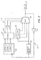
- FIGS 2 and 3 illustrate two slightly different implementations of a modulated clock in accordance with the invention.
- the clock 10 comprises a minimum delay circuit 22 and an inverter 20 coupled in a ring configuration. Those skilled in the art will appreciate that any odd number of inverters can be provided in place of the single inverter 20 illustrated.
- the minimum delay 22 sets the maximum clock rate that can be produced by the clock. Preferably, this delay will be set to provide the maximum clock rate at which the secure microprocessor can be operated.
- the substantially random modulation circuit 12 that modulates clock 10 comprises a series of delay stages 24, a multiplexer 26, a plurality of linear feedback shift register generators (LFSRGs) 28 and, optionally, a substitution box (S-Box) 30.
- the LFSRGs and S-Box provide control signals that are used by multiplexer 26 to select one of the delays provided by delay stages 24 for each clock pulse.
- the use of LFSRGs 28 enable the general requirements set forth above to be easily and controllably met. For example, the LFSRGs can be powered by a backup battery to retain their unpredictability even after application of a reset signal.
- the secure microprocessor system utilizes secret, unit dependent random keys held in registers, and the initial state of the LFSRGs are a function of or identical to one or more of these key registers, then maximum unit-dependent unpredictability can be provided. Further, exact minimum and maximum delays around the ring can be calculated for the implementations of Figures 2 and 3, facilitating reliable manufacture and operation of the circuits.
- the preferred embodiment of the present invention mixes the LFSRG outputs to provide a combined three-bit control word that is nonlinear and is used to select a delay value.
- a three-bit wide, eight entry deep lookup table can be used to provide the mixing. The lookup table maps a three-bit input (one bit from each of LFSRG 0, LFSRG 1, and LFSRG 2) into a new three-bit output in a highly nonlinear fashion.
- a substitution box (S-Box) 30 is used to derive the lookup table.
- S-Boxes The design of suitable S-Boxes is well known in the art. One approach is disclosed in C. Adams and S. Tavares, "The Structured Design of Cryptographically Good S-Boxes," Journal of Cryptology , 3 (1990), pp. 27-41, describing a procedure for constructing S-Boxes that are bijective, highly nonlinear, possess the strict avalanche criterion, and have output bits which act (virtually) independently when any single input bit is complemented. S-Boxes can also be generated algorithmically, as set forth in U.S. Patent 5,214,704.
- a specific three-bit S-table that can be used in accordance with the present invention is: Input Output 0 1 1 2 2 6 3 5 4 4 5 7 6 3 7 0
- the S-Box chosen will output the nonlinear control signals to multiplexer 26 via lines 32, 34 and 36.
- the control signals will actuate multiplexer 26 to output one of eight delays from minimum delay 22 or delay gates 24 (D1 ... D7).
- the delay stages D1 ... D7 are provided in series, each stage adding an additional delay to the minimum delay provided by circuit 22.
- a more mathematically flexible maximum performance structure is provided. This structure does not require that the delay values be from a single delay line tapped at different points. Instead, each delay required is implemented in a parallel, discrete fashion.
- the output of multiplexer 26 is the unpredictable clock signal CLK which is used to clock a secure microprocessor, such as processor 14 illustrated in Figure 1.
- CLK clock signal is fed back within the ring oscillator for use in generating the next successive clock pulse.
- the desired substantially random clock CLK is provided.
- the modulator 12 must be a self-timed structure that self-initializes and then propagates a change in logic state around a path of variable length (i.e., the ring oscillator). This path must effectively change length under the control of the pseudorandom data source provided by LFSRGs 28 and S-Box 30.
- the LFSRGs themselves must change state with each cycle of the modulator, and are therefore part of the modulator self-timing.
- the pseudorandom bitstream output from S-Box 30 must vary the delay length of the ring oscillator between some minimum delay T min and some maximum delay T max . This structure will guarantee bounds on output frequency, while allowing characteristics of the modulation bitstream to determine all other statistics such as distribution and average.
- Long-term randomness requires a long generator that can produce many long runs of ones or zeros. Short-term randomness must come from a separate generator that is much shorter, but still long enough that it will not repeat during long runs of ones or zeros from the long-term generator. The length of these two generators must be carefully controlled so that they do not easily relate to each other.
- the provision of a medium-term generator facilitates the provision of a random bitstream, when combined with the short and long-term generators to form a clock modulating bitstream.
- LFSRG 0 provides the least significant bit of modulator period word, and has a long length such as 2 40 -1, or 1.1 x 10 12 .
- LFSRG 1 is of medium length such as 2 32 -1, or 4.3 x 10 9 , and provides the second period word bit.
- LFSRG 2 has a short length such as 2 6 -1, or 127. The length of the LFSRGs are all relatively prime to each other, and will not interact in a simple way.
- the repetition periods of these generators are 1.1 x 10 5 seconds (1.27 days), 4.3 x 10 2 seconds (seven minutes, nine seconds), and 12.7 microseconds. It is noted that in selecting the lengths of the LFSRGs, attention must be paid to their interaction such that there are no periods of modulation inactivity.
- delay gates 24 Attention must also be paid to the specific delays provided by delay gates 24. If all gate delays D in the ring oscillator are identical, then the modulation will produce a substantially randomly varying but regular set of output frequencies. The period of the Mth output will always be a multiple of this basic gate delay, M x D, where M is modulated by taking on different integer values. If the individual gate delays are designed to be not identical, then a less regular output frequency set will result. These different gate delays must have a set of delays with complex interrelationships for all M possible values of modulation.
- variable frequency source 10 Various alternate implementations can be provided for the variable frequency source 10. Some of these are illustrated in Figures 4-7.
- a plurality of fixed digital or analog frequency sources 40 (f 1 , f 2 ... f n ) are randomly selectable by a selector 42 by a random control signal input to terminal 44.
- the randomly selected output frequencies are conditioned (e.g., deglitched) in a conditioning circuit 46 which outputs the "modulated" clock for control of the crypto processor.
- a single frequency source 50 is modulated by random modulation input to terminal 52.
- the resultant modulated clock is used to control the crypto processor.
- Frequency source 50 can comprise an analog circuit, such as a voltage controlled oscillator, voltage controlled crystal oscillator, current controlled oscillator, Colpitts oscillator, Hartley oscillator, or the like. Any such analog oscillator should use a linear mode transistor. Variable analog delays can also be used, wherein real or parasitic capacitors are relied on to establish different delay periods as well known in the art. In a digital implementation, any type of ring oscillator can be used for single frequency source 50.
- Figure 6 illustrates an embodiment in which tapped series delays generally designated 60 (D1, D2, ... DN) are introduced in the path of an input clock signal.
- a selector 62 selects the clock signal at random delay points in response to a random control signal input to terminal 64.
- the "modulated" output clock is used to clock the crypto processor.
- the delays can be provided by either analog or digital variable delay elements well known in the art.
- FIG. 7 illustrates an embodiment in which different parallel delays generally designated 70 (D1, D2, ... DN) are selected by a selector 72 in response to a random control signal applied to terminal 74.
- each of the delays 70 has a different duration and can comprise any analog or digital delay element known in the art.
- the "modulated" clock output from selector 72 is used to control the crypto processor.
- a clock signal is modulated to provide a substantially random and unpredictable series of clock pulses for clocking a secure microprocessor.
- the modulation behavior is designed to resist analysis attempts of a pirate.
Landscapes
- Engineering & Computer Science (AREA)
- Computer Security & Cryptography (AREA)
- Computer Networks & Wireless Communication (AREA)
- Signal Processing (AREA)
- Physics & Mathematics (AREA)
- Theoretical Computer Science (AREA)
- General Physics & Mathematics (AREA)
- Nonlinear Science (AREA)
- Power Engineering (AREA)
- Computer Hardware Design (AREA)
- General Engineering & Computer Science (AREA)
- Condensed Matter Physics & Semiconductors (AREA)
- Microelectronics & Electronic Packaging (AREA)
- Stabilization Of Oscillater, Synchronisation, Frequency Synthesizers (AREA)
- Channel Selection Circuits, Automatic Tuning Circuits (AREA)
- Selective Calling Equipment (AREA)
- Two-Way Televisions, Distribution Of Moving Picture Or The Like (AREA)
- Pulse Circuits (AREA)
- Synchronisation In Digital Transmission Systems (AREA)
- Storage Device Security (AREA)
- Executing Machine-Instructions (AREA)
- Multi Processors (AREA)
- Microcomputers (AREA)
Applications Claiming Priority (2)
| Application Number | Priority Date | Filing Date | Title |
|---|---|---|---|
| US167782 | 1993-12-21 | ||
| US08/167,782 US5404402A (en) | 1993-12-21 | 1993-12-21 | Clock frequency modulation for secure microprocessors |
Publications (3)
| Publication Number | Publication Date |
|---|---|
| EP0660562A2 EP0660562A2 (en) | 1995-06-28 |
| EP0660562A3 EP0660562A3 (en) | 1997-06-18 |
| EP0660562B1 true EP0660562B1 (en) | 2000-09-20 |
Family
ID=22608810
Family Applications (1)
| Application Number | Title | Priority Date | Filing Date |
|---|---|---|---|
| EP94118067A Expired - Lifetime EP0660562B1 (en) | 1993-12-21 | 1994-11-16 | Clock frequency modulation for secure microprocessors |
Country Status (8)
| Country | Link |
|---|---|
| US (1) | US5404402A (ja) |
| EP (1) | EP0660562B1 (ja) |
| JP (1) | JPH07239837A (ja) |
| KR (1) | KR100210524B1 (ja) |
| AT (1) | ATE196581T1 (ja) |
| DE (1) | DE69425952T2 (ja) |
| NO (1) | NO944432L (ja) |
| TW (1) | TW228042B (ja) |
Families Citing this family (73)
| Publication number | Priority date | Publication date | Assignee | Title |
|---|---|---|---|---|
| FR2745099B1 (fr) * | 1996-02-19 | 1998-03-27 | Sgs Thomson Microelectronics | Procede de sequencement d'un circuit integre |
| FR2745924B1 (fr) * | 1996-03-07 | 1998-12-11 | Bull Cp8 | Circuit integre perfectionne et procede d'utilisation d'un tel circuit integre |
| JP3683031B2 (ja) * | 1996-04-17 | 2005-08-17 | 株式会社リコー | プログラム保護装置 |
| JPH10222065A (ja) * | 1997-02-03 | 1998-08-21 | Nippon Telegr & Teleph Corp <Ntt> | 冪乗剰余演算方法及び装置 |
| US5923191A (en) * | 1997-05-08 | 1999-07-13 | Vlsi Technology, Inc. | Device and a method for monitoring a system clock signal |
| FR2765361B1 (fr) * | 1997-06-26 | 2001-09-21 | Bull Cp8 | Microprocesseur ou microcalculateur imprevisible |
| CA2316227C (en) * | 1998-01-02 | 2009-08-11 | Cryptography Research, Inc. | Leak-resistant cryptographic method and apparatus |
| US7587044B2 (en) * | 1998-01-02 | 2009-09-08 | Cryptography Research, Inc. | Differential power analysis method and apparatus |
| US6327661B1 (en) | 1998-06-03 | 2001-12-04 | Cryptography Research, Inc. | Using unpredictable information to minimize leakage from smartcards and other cryptosystems |
| FR2776410B1 (fr) * | 1998-03-20 | 2002-11-15 | Gemplus Card Int | Dispositifs pour masquer les operations effectuees dans une carte a microprocesseur |
| CN100530025C (zh) * | 1998-05-29 | 2009-08-19 | 西门子公司 | 处理数据的方法和装置 |
| DE19828936A1 (de) * | 1998-05-29 | 1999-12-02 | Siemens Ag | Verfahren und Vorrichtung zum Verarbeiten von Daten |
| US20030118190A1 (en) * | 1998-05-29 | 2003-06-26 | Siemens Aktiengesellschaft | Method and apparatus for processing data where a part of the current supplied is supplied to an auxiliary circuit |
| IL139935A (en) * | 1998-06-03 | 2005-06-19 | Cryptography Res Inc | Des and other cryptographic processes with leak minimization for smartcards and other cryptosystems |
| EP1926241A3 (en) | 1998-06-03 | 2009-03-11 | Cryptography Research Inc. | Using unpredictable information to minimize leakage from smartcards and other cryptosystems |
| TW375721B (en) * | 1998-06-17 | 1999-12-01 | Ind Tech Res Inst | DES chip processor capable of executing data encryption standard (DES) operation |
| US6539092B1 (en) | 1998-07-02 | 2003-03-25 | Cryptography Research, Inc. | Leak-resistant cryptographic indexed key update |
| US6865675B1 (en) * | 1998-07-14 | 2005-03-08 | Koninklijke Philips Electronics N.V. | Method and apparatus for use of a watermark and a unique time dependent reference for the purpose of copy protection |
| DE19936938A1 (de) * | 1998-09-30 | 2000-04-06 | Philips Corp Intellectual Pty | Datenverarbeitungseinrichtung und Verfahren zu dessen Betrieb zum Verhindern einer differentiellen Stromverbrauchanalyse |
| FR2790347B1 (fr) * | 1999-02-25 | 2001-10-05 | St Microelectronics Sa | Procede de securisation d'un enchainement d'operations realisees par un circuit electronique dans le cadre de l'execution d'un algorithme |
| JP3827050B2 (ja) * | 1999-03-09 | 2006-09-27 | 株式会社ルネサステクノロジ | Icカードと半導体集積回路装置 |
| DE19921633A1 (de) * | 1999-05-10 | 2000-11-16 | Deutsche Telekom Ag | Verfahren zur Implementierung kryptographischer Algorithmen |
| US6804782B1 (en) * | 1999-06-11 | 2004-10-12 | General Instrument Corporation | Countermeasure to power attack and timing attack on cryptographic operations |
| JP2001094550A (ja) * | 1999-09-17 | 2001-04-06 | Toshiba Corp | 信号処理装置 |
| EP1098469B1 (de) * | 1999-11-03 | 2007-06-06 | Infineon Technologies AG | Kodiervorrichtung |
| DE19955601C2 (de) | 1999-11-18 | 2001-11-29 | Infineon Technologies Ag | Verfahren zur Durchführung von Auto-Refresh-Sequenzen an einem DRAM |
| JP3866105B2 (ja) * | 1999-12-02 | 2007-01-10 | インフィネオン テクノロジーズ アクチエンゲゼルシャフト | 暗号化機能を備えるマイクロプロセッサ装置 |
| ATE249664T1 (de) * | 2000-01-18 | 2003-09-15 | Infineon Technologies Ag | Mikroprozessoranordnung mit verschlüsselung |
| GB2365153A (en) * | 2000-01-28 | 2002-02-13 | Simon William Moore | Microprocessor resistant to power analysis with an alarm state |
| FR2808360B1 (fr) * | 2000-04-28 | 2002-06-28 | Gemplus Card Int | Procede de contre mesure dans un microcircuit mettant en oeuvre le procede et carte a puce comportant ledit microcircuit |
| JP4683442B2 (ja) * | 2000-07-13 | 2011-05-18 | 富士通フロンテック株式会社 | 処理装置および集積回路 |
| US7620832B2 (en) * | 2000-09-20 | 2009-11-17 | Mips Technologies, Inc. | Method and apparatus for masking a microprocessor execution signature |
| US6507247B2 (en) * | 2001-02-27 | 2003-01-14 | Corrent Corporation | Circuit and method for generating a variable frequency clock signal |
| DE10111435A1 (de) * | 2001-03-09 | 2002-09-26 | Infineon Technologies Ag | Vorrichtung und Verfahren zum Ausführen von Operationen mit einer einstellbaren Geschwindigkeit |
| US7318145B1 (en) | 2001-06-01 | 2008-01-08 | Mips Technologies, Inc. | Random slip generator |
| EP1293856A1 (fr) * | 2001-09-18 | 2003-03-19 | EM Microelectronic-Marin SA | Circuit Intégré sécurisé comprenant des parties à caractère confidentiel, et procédé pour sa mise en action |
| JP4045777B2 (ja) * | 2001-10-30 | 2008-02-13 | 株式会社日立製作所 | 情報処理装置 |
| FR2833724A1 (fr) * | 2001-12-13 | 2003-06-20 | Canal Plus Technologies | Composant electronique numerique protege contre des analyses de type electrique et/ou electromagnetique, notamment dans le domaine de la carte a puce |
| DE10162309A1 (de) * | 2001-12-19 | 2003-07-03 | Philips Intellectual Property | Verfahren und Anordnung zur Erhöhung der Sicherheit von Schaltkreisen gegen unbefugten Zugriff |
| JP3672874B2 (ja) * | 2002-01-25 | 2005-07-20 | Necマイクロシステム株式会社 | データ処理装置 |
| JP2003244104A (ja) * | 2002-02-21 | 2003-08-29 | Ntt Advanced Technology Corp | 漏洩電磁波による情報再生の防止方法、及び情報機器 |
| DE10217291B4 (de) * | 2002-04-18 | 2005-09-29 | Infineon Technologies Ag | Datenverarbeitungsvorrichtung und Verfahren zum Betreiben eines Datenverarbeitungsmoduls |
| US7248696B2 (en) * | 2002-09-12 | 2007-07-24 | International Business Machines Corporation | Dynamic system bus encryption using improved differential transitional encoding |
| WO2004053684A2 (en) * | 2002-12-12 | 2004-06-24 | Arm Limited | Processing activity masking in a data processing system |
| EP1496641A3 (en) * | 2003-07-07 | 2005-03-02 | Sony Corporation | Cryptographic processing apparatus, cryptographic processing method and computer program |
| TWI249092B (en) * | 2003-08-12 | 2006-02-11 | Novatek Microelectronics Corp | A frequency synthesizer using interpolation and linear feedback shift register (LFSR) |
| US7502468B2 (en) * | 2003-09-02 | 2009-03-10 | Ncipher Corporation Ltd. | Method and system for generating a cryptographically random number stream |
| EP1513285A1 (en) * | 2003-09-05 | 2005-03-09 | Mediacrypt AG | Method for generating pseudo-random sequence |
| FR2861474B1 (fr) * | 2003-10-24 | 2007-04-27 | Atmel Corp | Procede et appareil pour une periode de traitement variable dans un circuit integre |
| US7382824B1 (en) * | 2004-08-13 | 2008-06-03 | Emc Corporaration | Method and apparatus for accurate modeling of multi-domain clock interfaces |
| US7574137B1 (en) * | 2006-05-05 | 2009-08-11 | The United States Of America As Represented By The Administrator Of The National Aeronautics And Space Administration | Multi-wavelength time-coincident optical communications system and methods thereof |
| EP1855402A1 (en) * | 2006-05-11 | 2007-11-14 | Koninklijke Philips Electronics N.V. | Transmission, reception and synchronisation of two data streams |
| US8301890B2 (en) * | 2006-08-10 | 2012-10-30 | Inside Secure | Software execution randomization |
| US7613907B2 (en) * | 2006-08-11 | 2009-11-03 | Atmel Corporation | Embedded software camouflage against code reverse engineering |
| US7554865B2 (en) * | 2006-09-21 | 2009-06-30 | Atmel Corporation | Randomizing current consumption in memory devices |
| US7613915B2 (en) * | 2006-11-09 | 2009-11-03 | BroadOn Communications Corp | Method for programming on-chip non-volatile memory in a secure processor, and a device so programmed |
| US8255702B1 (en) * | 2009-12-03 | 2012-08-28 | Altera Corporation | Programmable logic device with improved security |
| US8522052B1 (en) | 2010-04-07 | 2013-08-27 | Xilinx, Inc. | Method and integrated circuit for secure encryption and decryption |
| US9213835B2 (en) * | 2010-04-07 | 2015-12-15 | Xilinx, Inc. | Method and integrated circuit for secure encryption and decryption |
| US20110299678A1 (en) * | 2010-06-07 | 2011-12-08 | Alexander Roger Deas | Secure means for generating a specific key from unrelated parameters |
| FR2980657B1 (fr) * | 2011-09-28 | 2014-06-20 | Oberthur Technologies | Circuit electronique presentant une desynchronisation materielle au sein d'une periode d'horloge |
| US9755822B2 (en) | 2013-06-19 | 2017-09-05 | Cryptography Research, Inc. | Countermeasure to power analysis attacks through time-varying impedance of power delivery networks |
| IL234956A (en) | 2014-10-02 | 2017-10-31 | Kaluzhny Uri | Data bus protection with enhanced key entropy |
| EP3147774A1 (fr) * | 2015-09-25 | 2017-03-29 | Gemalto Sa | Generateur d'horloge aleatoire |
| US10958414B2 (en) * | 2016-02-23 | 2021-03-23 | Google Llc | Clock period randomization for defense against cryptographic attacks |
| US10019571B2 (en) * | 2016-03-13 | 2018-07-10 | Winbond Electronics Corporation | Protection from side-channel attacks by varying clock delays |
| CN105894079B (zh) * | 2016-04-22 | 2019-03-15 | 上海东软载波微电子有限公司 | 时钟加扰电路 |
| US10255462B2 (en) | 2016-06-17 | 2019-04-09 | Arm Limited | Apparatus and method for obfuscating power consumption of a processor |
| US10459477B2 (en) * | 2017-04-19 | 2019-10-29 | Seagate Technology Llc | Computing system with power variation attack countermeasures |
| US10200192B2 (en) | 2017-04-19 | 2019-02-05 | Seagate Technology Llc | Secure execution environment clock frequency hopping |
| JP2019012944A (ja) * | 2017-06-30 | 2019-01-24 | 株式会社デンソー | クロック信号生成回路 |
| CN109254617B (zh) * | 2017-07-14 | 2020-11-06 | 华为技术有限公司 | 时钟信号产生方法以及装置 |
| CN110726483B (zh) * | 2019-09-30 | 2021-10-08 | 安徽问天量子科技股份有限公司 | 抵御雪崩过渡区攻击的装置及方法 |
Family Cites Families (7)
| Publication number | Priority date | Publication date | Assignee | Title |
|---|---|---|---|---|
| US4392021A (en) * | 1980-07-28 | 1983-07-05 | Technical Communications Corporation | Secure facsimile transmission system using time-delay modulation |
| IE54401B1 (en) * | 1982-05-21 | 1989-09-27 | Marconi Co Ltd | Random sequence generators |
| US4819164A (en) * | 1983-12-12 | 1989-04-04 | Texas Instruments Incorporated | Variable frequency microprocessor clock generator |
| US4905176A (en) * | 1988-10-28 | 1990-02-27 | International Business Machines Corporation | Random number generator circuit |
| FR2638869B1 (fr) * | 1988-11-10 | 1990-12-21 | Sgs Thomson Microelectronics | Dispositif de securite contre la detection non autorisee de donnees protegees |
| US5001756A (en) * | 1989-08-11 | 1991-03-19 | Motorola, Inc. | Decryption device with variable clock |
| US5214704A (en) * | 1989-10-04 | 1993-05-25 | Teledyne Industries, Inc. | Nonlinear dynamic substitution devices and methods for block substitutions |
-
1993
- 1993-12-21 US US08/167,782 patent/US5404402A/en not_active Expired - Lifetime
-
1994
- 1994-01-17 TW TW083100318A patent/TW228042B/zh active
- 1994-11-16 AT AT94118067T patent/ATE196581T1/de not_active IP Right Cessation
- 1994-11-16 DE DE69425952T patent/DE69425952T2/de not_active Expired - Fee Related
- 1994-11-16 EP EP94118067A patent/EP0660562B1/en not_active Expired - Lifetime
- 1994-11-18 NO NO944432A patent/NO944432L/no unknown
- 1994-12-05 KR KR1019940032786A patent/KR100210524B1/ko not_active IP Right Cessation
- 1994-12-19 JP JP6333757A patent/JPH07239837A/ja active Pending
Also Published As
| Publication number | Publication date |
|---|---|
| EP0660562A3 (en) | 1997-06-18 |
| TW228042B (en) | 1994-08-11 |
| KR950023026A (ko) | 1995-07-28 |
| DE69425952D1 (de) | 2000-10-26 |
| JPH07239837A (ja) | 1995-09-12 |
| DE69425952T2 (de) | 2001-05-10 |
| US5404402A (en) | 1995-04-04 |
| ATE196581T1 (de) | 2000-10-15 |
| NO944432L (no) | 1995-06-22 |
| EP0660562A2 (en) | 1995-06-28 |
| KR100210524B1 (ko) | 1999-07-15 |
| NO944432D0 (no) | 1994-11-18 |
Similar Documents
| Publication | Publication Date | Title |
|---|---|---|
| EP0660562B1 (en) | Clock frequency modulation for secure microprocessors | |
| US5115467A (en) | Signal encryption apparatus for generating common and distinct keys | |
| US5077793A (en) | Residue number encryption and decryption system | |
| AU685416B2 (en) | Methods and apparatus for uniquely encrypting data at a plurality of data transmission sites | |
| EP0096724B1 (en) | Sync suppression scrambling of television signals for subscription tv | |
| US4944006A (en) | Secure data packet transmission system and method | |
| USRE33189E (en) | Security system for SSTV encryption | |
| US4484027A (en) | Security system for SSTV encryption | |
| US4887296A (en) | Cryptographic system for direct broadcast satellite system | |
| US5345508A (en) | Method and apparatus for variable-overhead cached encryption | |
| US4791669A (en) | Encryption/decryption system | |
| EP0713621B1 (en) | Method and apparatus for uniquely encrypting a plurality of services at a transmission site | |
| EP0994598A1 (en) | Cryptation system for packet switching networks based on digital chaotic models | |
| EP1260052B1 (en) | Cryptographic communication process and apparatus | |
| US4649419A (en) | Pseudo-random binary sequency generator | |
| US5243650A (en) | Method and apparatus for encryption/decryption of digital multisound in television | |
| KR100662667B1 (ko) | 동기 스트림 암호 | |
| WO1995006373A1 (en) | Method and apparatus for decryption using cache storage | |
| US4811394A (en) | Variable starting state scrambling circuit | |
| US4464678A (en) | Time window key system for video scrambling | |
| WO2005034514A1 (en) | Portable security module pairing | |
| JP2004515159A (ja) | 条件付きアクセス・システムのためのしきい値暗号方法およびシステム | |
| EP0116082B1 (en) | Secure coding and decoding system and method for television program signals | |
| EP0148263A4 (en) | LIKELIHOOD CRUSHERS AND METHODS FOR CREDIBILITY. | |
| KR100226625B1 (ko) | 비디오 신호의 암호화 장치 |
Legal Events
| Date | Code | Title | Description |
|---|---|---|---|
| PUAI | Public reference made under article 153(3) epc to a published international application that has entered the european phase |
Free format text: ORIGINAL CODE: 0009012 |
|
| AK | Designated contracting states |
Kind code of ref document: A2 Designated state(s): AT BE CH DE DK ES FR GB IE IT LI NL SE |
|
| PUAL | Search report despatched |
Free format text: ORIGINAL CODE: 0009013 |
|
| AK | Designated contracting states |
Kind code of ref document: A3 Designated state(s): AT BE CH DE DK ES FR GB IE IT LI NL SE |
|
| 17P | Request for examination filed |
Effective date: 19971107 |
|
| 17Q | First examination report despatched |
Effective date: 19971211 |
|
| RAP1 | Party data changed (applicant data changed or rights of an application transferred) |
Owner name: GENERAL INSTRUMENT CORPORATION |
|
| RAP1 | Party data changed (applicant data changed or rights of an application transferred) |
Owner name: GENERAL SEMICONDUCTOR, INC. |
|
| RAP1 | Party data changed (applicant data changed or rights of an application transferred) |
Owner name: GENERAL INSTRUMENT CORPORATION |
|
| GRAG | Despatch of communication of intention to grant |
Free format text: ORIGINAL CODE: EPIDOS AGRA |
|
| GRAG | Despatch of communication of intention to grant |
Free format text: ORIGINAL CODE: EPIDOS AGRA |
|
| GRAH | Despatch of communication of intention to grant a patent |
Free format text: ORIGINAL CODE: EPIDOS IGRA |
|
| GRAH | Despatch of communication of intention to grant a patent |
Free format text: ORIGINAL CODE: EPIDOS IGRA |
|
| GRAA | (expected) grant |
Free format text: ORIGINAL CODE: 0009210 |
|
| AK | Designated contracting states |
Kind code of ref document: B1 Designated state(s): AT BE CH DE DK ES FR GB IE IT LI NL SE |
|
| PG25 | Lapsed in a contracting state [announced via postgrant information from national office to epo] |
Ref country code: LI Free format text: LAPSE BECAUSE OF FAILURE TO SUBMIT A TRANSLATION OF THE DESCRIPTION OR TO PAY THE FEE WITHIN THE PRESCRIBED TIME-LIMIT Effective date: 20000920 Ref country code: IT Free format text: LAPSE BECAUSE OF FAILURE TO SUBMIT A TRANSLATION OF THE DESCRIPTION OR TO PAY THE FEE WITHIN THE PRE;WARNING: LAPSES OF ITALIAN PATENTS WITH EFFECTIVE DATE BEFORE 2007 MAY HAVE OCCURRED AT ANY TIME BEFORE 2007. THE CORRECT EFFECTIVE DATE MAY BE DIFFERENT FROM THE ONE RECORDED.SCRIBED TIME-LIMIT Effective date: 20000920 Ref country code: ES Free format text: THE PATENT HAS BEEN ANNULLED BY A DECISION OF A NATIONAL AUTHORITY Effective date: 20000920 Ref country code: CH Free format text: LAPSE BECAUSE OF FAILURE TO SUBMIT A TRANSLATION OF THE DESCRIPTION OR TO PAY THE FEE WITHIN THE PRESCRIBED TIME-LIMIT Effective date: 20000920 Ref country code: BE Free format text: LAPSE BECAUSE OF FAILURE TO SUBMIT A TRANSLATION OF THE DESCRIPTION OR TO PAY THE FEE WITHIN THE PRESCRIBED TIME-LIMIT Effective date: 20000920 Ref country code: AT Free format text: LAPSE BECAUSE OF FAILURE TO SUBMIT A TRANSLATION OF THE DESCRIPTION OR TO PAY THE FEE WITHIN THE PRESCRIBED TIME-LIMIT Effective date: 20000920 |
|
| REF | Corresponds to: |
Ref document number: 196581 Country of ref document: AT Date of ref document: 20001015 Kind code of ref document: T |
|
| REG | Reference to a national code |
Ref country code: CH Ref legal event code: EP |
|
| REF | Corresponds to: |
Ref document number: 69425952 Country of ref document: DE Date of ref document: 20001026 |
|
| REG | Reference to a national code |
Ref country code: IE Ref legal event code: FG4D |
|
| ET | Fr: translation filed | ||
| PG25 | Lapsed in a contracting state [announced via postgrant information from national office to epo] |
Ref country code: IE Free format text: LAPSE BECAUSE OF NON-PAYMENT OF DUE FEES Effective date: 20001116 |
|
| PG25 | Lapsed in a contracting state [announced via postgrant information from national office to epo] |
Ref country code: SE Free format text: LAPSE BECAUSE OF FAILURE TO SUBMIT A TRANSLATION OF THE DESCRIPTION OR TO PAY THE FEE WITHIN THE PRESCRIBED TIME-LIMIT Effective date: 20001220 Ref country code: DK Free format text: LAPSE BECAUSE OF FAILURE TO SUBMIT A TRANSLATION OF THE DESCRIPTION OR TO PAY THE FEE WITHIN THE PRESCRIBED TIME-LIMIT Effective date: 20001220 |
|
| REG | Reference to a national code |
Ref country code: CH Ref legal event code: PL |
|
| PLBE | No opposition filed within time limit |
Free format text: ORIGINAL CODE: 0009261 |
|
| STAA | Information on the status of an ep patent application or granted ep patent |
Free format text: STATUS: NO OPPOSITION FILED WITHIN TIME LIMIT |
|
| 26N | No opposition filed | ||
| REG | Reference to a national code |
Ref country code: IE Ref legal event code: MM4A |
|
| REG | Reference to a national code |
Ref country code: GB Ref legal event code: IF02 |
|
| PGFP | Annual fee paid to national office [announced via postgrant information from national office to epo] |
Ref country code: GB Payment date: 20041004 Year of fee payment: 11 |
|
| PGFP | Annual fee paid to national office [announced via postgrant information from national office to epo] |
Ref country code: NL Payment date: 20041006 Year of fee payment: 11 |
|
| PGFP | Annual fee paid to national office [announced via postgrant information from national office to epo] |
Ref country code: FR Payment date: 20041105 Year of fee payment: 11 |
|
| PG25 | Lapsed in a contracting state [announced via postgrant information from national office to epo] |
Ref country code: GB Free format text: LAPSE BECAUSE OF NON-PAYMENT OF DUE FEES Effective date: 20051116 |
|
| PGFP | Annual fee paid to national office [announced via postgrant information from national office to epo] |
Ref country code: DE Payment date: 20051130 Year of fee payment: 12 |
|
| PG25 | Lapsed in a contracting state [announced via postgrant information from national office to epo] |
Ref country code: NL Free format text: LAPSE BECAUSE OF NON-PAYMENT OF DUE FEES Effective date: 20060601 |
|
| GBPC | Gb: european patent ceased through non-payment of renewal fee |
Effective date: 20051116 |
|
| PG25 | Lapsed in a contracting state [announced via postgrant information from national office to epo] |
Ref country code: FR Free format text: LAPSE BECAUSE OF NON-PAYMENT OF DUE FEES Effective date: 20060731 |
|
| NLV4 | Nl: lapsed or anulled due to non-payment of the annual fee |
Effective date: 20060601 |
|
| REG | Reference to a national code |
Ref country code: FR Ref legal event code: ST Effective date: 20060731 |
|
| PG25 | Lapsed in a contracting state [announced via postgrant information from national office to epo] |
Ref country code: DE Free format text: LAPSE BECAUSE OF NON-PAYMENT OF DUE FEES Effective date: 20070601 |
|
| P01 | Opt-out of the competence of the unified patent court (upc) registered |
Effective date: 20230520 |