EP0660469A2 - Herstellungsverfahren eines wellenlänge selektiven elektrooptischen Gitters für DFB/DBR Laser - Google Patents
Herstellungsverfahren eines wellenlänge selektiven elektrooptischen Gitters für DFB/DBR Laser Download PDFInfo
- Publication number
- EP0660469A2 EP0660469A2 EP94309007A EP94309007A EP0660469A2 EP 0660469 A2 EP0660469 A2 EP 0660469A2 EP 94309007 A EP94309007 A EP 94309007A EP 94309007 A EP94309007 A EP 94309007A EP 0660469 A2 EP0660469 A2 EP 0660469A2
- Authority
- EP
- European Patent Office
- Prior art keywords
- accordance
- waveguide
- depositing
- grating
- cladding
- Prior art date
- Legal status (The legal status is an assumption and is not a legal conclusion. Google has not performed a legal analysis and makes no representation as to the accuracy of the status listed.)
- Withdrawn
Links
Images

Classifications
-
- H—ELECTRICITY
- H01—ELECTRIC ELEMENTS
- H01S—DEVICES USING THE PROCESS OF LIGHT AMPLIFICATION BY STIMULATED EMISSION OF RADIATION [LASER] TO AMPLIFY OR GENERATE LIGHT; DEVICES USING STIMULATED EMISSION OF ELECTROMAGNETIC RADIATION IN WAVE RANGES OTHER THAN OPTICAL
- H01S5/00—Semiconductor lasers
- H01S5/10—Construction or shape of the optical resonator, e.g. extended or external cavity, coupled cavities, bent-guide, varying width, thickness or composition of the active region
- H01S5/12—Construction or shape of the optical resonator, e.g. extended or external cavity, coupled cavities, bent-guide, varying width, thickness or composition of the active region the resonator having a periodic structure, e.g. in distributed feedback [DFB] lasers
- H01S5/125—Distributed Bragg reflector [DBR] lasers
-
- H—ELECTRICITY
- H01—ELECTRIC ELEMENTS
- H01S—DEVICES USING THE PROCESS OF LIGHT AMPLIFICATION BY STIMULATED EMISSION OF RADIATION [LASER] TO AMPLIFY OR GENERATE LIGHT; DEVICES USING STIMULATED EMISSION OF ELECTROMAGNETIC RADIATION IN WAVE RANGES OTHER THAN OPTICAL
- H01S5/00—Semiconductor lasers
- H01S5/10—Construction or shape of the optical resonator, e.g. extended or external cavity, coupled cavities, bent-guide, varying width, thickness or composition of the active region
- H01S5/12—Construction or shape of the optical resonator, e.g. extended or external cavity, coupled cavities, bent-guide, varying width, thickness or composition of the active region the resonator having a periodic structure, e.g. in distributed feedback [DFB] lasers
-
- H—ELECTRICITY
- H01—ELECTRIC ELEMENTS
- H01S—DEVICES USING THE PROCESS OF LIGHT AMPLIFICATION BY STIMULATED EMISSION OF RADIATION [LASER] TO AMPLIFY OR GENERATE LIGHT; DEVICES USING STIMULATED EMISSION OF ELECTROMAGNETIC RADIATION IN WAVE RANGES OTHER THAN OPTICAL
- H01S5/00—Semiconductor lasers
- H01S5/06—Arrangements for controlling the laser output parameters, e.g. by operating on the active medium
- H01S5/062—Arrangements for controlling the laser output parameters, e.g. by operating on the active medium by varying the potential of the electrodes
- H01S5/0625—Arrangements for controlling the laser output parameters, e.g. by operating on the active medium by varying the potential of the electrodes in multi-section lasers
- H01S5/06255—Controlling the frequency of the radiation
- H01S5/06256—Controlling the frequency of the radiation with DBR-structure
-
- H—ELECTRICITY
- H01—ELECTRIC ELEMENTS
- H01S—DEVICES USING THE PROCESS OF LIGHT AMPLIFICATION BY STIMULATED EMISSION OF RADIATION [LASER] TO AMPLIFY OR GENERATE LIGHT; DEVICES USING STIMULATED EMISSION OF ELECTROMAGNETIC RADIATION IN WAVE RANGES OTHER THAN OPTICAL
- H01S5/00—Semiconductor lasers
- H01S5/10—Construction or shape of the optical resonator, e.g. extended or external cavity, coupled cavities, bent-guide, varying width, thickness or composition of the active region
- H01S5/1046—Comprising interactions between photons and plasmons, e.g. by a corrugated surface
-
- H—ELECTRICITY
- H01—ELECTRIC ELEMENTS
- H01S—DEVICES USING THE PROCESS OF LIGHT AMPLIFICATION BY STIMULATED EMISSION OF RADIATION [LASER] TO AMPLIFY OR GENERATE LIGHT; DEVICES USING STIMULATED EMISSION OF ELECTROMAGNETIC RADIATION IN WAVE RANGES OTHER THAN OPTICAL
- H01S5/00—Semiconductor lasers
- H01S5/10—Construction or shape of the optical resonator, e.g. extended or external cavity, coupled cavities, bent-guide, varying width, thickness or composition of the active region
- H01S5/12—Construction or shape of the optical resonator, e.g. extended or external cavity, coupled cavities, bent-guide, varying width, thickness or composition of the active region the resonator having a periodic structure, e.g. in distributed feedback [DFB] lasers
- H01S5/1231—Grating growth or overgrowth details
Definitions
- the present invention relates to a method for the preparation of a wavelength selective electro-optic grating for DFB/DBR lasers and related structures wherein etched corrugation wavelength gratings are replaced with a grating formed by periodically modulating the index of refraction of the cladding employed or the waveguide itself.
- Scanning electron micrographs in distributed feedback lasers reveal a corrugated interface between a higher index core material and a lower index cladding material.
- each bump reflects a small portion of the light. If the beam's wavelength is not close to the Bragg wavelength, all the reflections are out of phase and interfere destructively. At the Bragg wavelength, all reflections add in phase, so leading to a large cumulative reflection.
- the control of output wavelength of semiconductor lasers in distributed feedback (DFB) and tuning in distributed Bragg reflector (DBR) based lasers is achieved by means of the incorporation therein of the above-noted corrugated waveguide grating.
- DBR distributed feedback
- gratings of this type are typically installed by etching back a portion of the active layer and exposing the surface of an underlying passive waveguide.
- the grating may be installed in the substrate prior to the growth of the waveguide.
- an interference pattern formed by ultraviolet lasers is typically used to expose photoresist deposited on the exposed waveguide. The developed photoresist then forms the mask for etching the grating corrugation.
- the exposed portion of the structure is then regrown and contacts attached for operation.
- the grating is usually installed prior to growth of the active layer or waveguide. This end is typically attained by using an interference pattern, as described above, to expose photoresist deposited on the exposed passive waveguide. The exposed photoresist forms a mask for etching the corrugation.
- the active layer is then grown over the grating and suitable contacts are added to effect operation.
- the etched corrugation waveguide grating in the aforementioned structures is replaced with a grating formed by periodically modulating the index of refraction of either the cladding material or the waveguide.
- the modulated media chosen may be either bulk material or, more specifically, contain quantum well structures. In the case of the latter, it would effect large changes in the index of refraction by means of the quantum confined Stark effect or phase space absorption quenching with the application of an electric field. In the case of bulk material, current injection is the preferred mode of operation since the field induced change in the refractive index (Franz-Keldysh effect) is less efficient.
- the periodicity of the described device is established by means of conducting media, for example, metal, conductive polymer, etc.
- the conductive media is employed in the form of strip lines through which current is passed or an electric field is established through the media. Alternatively, periodicity may be established simply by the plasmon interaction of the periodically spaced conductive strip lines with the media.
- the first step in the practice of the present invention involves selection of a suitable substrate material.
- Most of the optoelectronic devices currently manufactured are designed for long wavelength systems (1.3 and 1.55 micrometers) and are typically fabricated from indium gallium arsenide phosphide materials on indium phosphide substrates. However, in some cases aluminum gallium arsenide/gallium arsenide substrates are employed for short wavelength systems.
- the substrate chosen is normally n-doped.
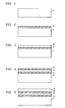
- Fig. 1 depicts a typical semi-insulating n-type indium phosphide substrate member 11 in front elevational view.
- an n-type buffer layer (conducting plane) 12 is deposited upon the substrate 11 by conventional epitaxial growth techniques. This contact layer is required in those instances in which a semi-insulating substrate is used to provide the required conductivity.
- the epitaxial growth process preserves the crystalline symmetry of the substrate. Typical procedures suitable for this purpose include molecular beam epitaxy using only elemental sources or metal organic chemical vapor deposition using easily vaporized molecular sources.
- a waveguide 13 shown in Fig. 3.
- the waveguide selected for use in the practice of the present invention may be chosen from among any of the conventional prior art materials commonly used for this purpose and may comprise bulk materials or quantum well layers.
- the waveguide is grown in the base structure in an appropriate stoichiometry for achieving or propagating a particular wavelength suitable for waveguiding properties.
- the thickness of the waveguide is dictated by considerations relating to the optical mode desired.
- n-type contact layer (conductive plane) 14 is deposited upon waveguide 13 as shown in Fig. 4.
- a laser 15 is deposited upon conductive layer 14, as shown in Fig. 5, by conventional epitaxial growth techniques.
- the laser is selected from among any of the materials commonly employed in distributed feedback (DFB) lasers and distributed Bragg reflector (DBR) lasers. Typical of such materials are the III-V semiconductor materials such as indium gallium arsenide phosphide.
- the next step in the fabrication of the desired structure involves etching down the assembly to expose the waveguide materials.
- This end may be effected, for example, by anisotropic dry etching or low frequency plasma etching in which the direction of the ion bombardment enhances the etch rate.
- etchants may be chosen for this purpose. Typical etchants suitable for such use are HCI, Br:CH 3 0H, H 2 SO 4 :H 2 0 2 and HBr:H 2 0 2 for wet etching and CF 2 CI 2 , CH 4 :H 2 and CH 4 H 2 for dry etching.
- cladding 16 is deposited thereon.
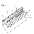
- a conductive material is deposited upon the cladding region 16 in the form of a grating 17 as shown in Fig. 8 by photolithographic techniques.
- a front elevational view, in perspective, of the structure of Fig. 8 is shown in Fig. 9.
- the conductive material selected for use in the practice of the present invention may be chosen from among any of the conventional prior art materials used for this purpose and may comprise metals, semiconductors, or polymers. Polymer systems suitable for this purpose evidence metallic conductivity, are soluble, processable and environmentally stable. The most commonly used material for this purpose is polyaniline of the general formula:
- This polymer, in the undoped form, is solution processable from both organic and aqueous acid solutions.
- the conductivity of the polyaniline does not degrade upon exposure to ambient conditions.
- Numerous derivatives of the material are also feasible since substituents such as alkyl groups can be easily incorporated on either the aromatic rings or the nitrogen atoms. This permits tailoring of the properties of the polyanilines.
- the thickness and refractive index of the cladding/spacer layer for the conductive material is determined by the optical mode required and would be apparent to those skilled in the art.
- the structures prepared in the described manner are suitable for use in a typical DBR laser system.
- the application of a difference of potential across the cladding periodically will result in the preparation of a grating of controlled refractive index, such control being attained by regulation of the voltage bias.
- the prime advantage of this technology resides in the substitution of conventional prior art gratings with an elctro-optic grating which enhances the lifetime of the device and improves the yield while reducing processing costs.
Landscapes
- Physics & Mathematics (AREA)
- Condensed Matter Physics & Semiconductors (AREA)
- General Physics & Mathematics (AREA)
- Electromagnetism (AREA)
- Optics & Photonics (AREA)
- Semiconductor Lasers (AREA)
Applications Claiming Priority (2)
| Application Number | Priority Date | Filing Date | Title |
|---|---|---|---|
| US171126 | 1993-12-21 | ||
| US08/171,126 US6194240B1 (en) | 1993-12-21 | 1993-12-21 | Method for fabrication of wavelength selective electro-optic grating for DFB/DBR lasers |
Publications (2)
| Publication Number | Publication Date |
|---|---|
| EP0660469A2 true EP0660469A2 (de) | 1995-06-28 |
| EP0660469A3 EP0660469A3 (de) | 1995-11-29 |
Family
ID=22622634
Family Applications (1)
| Application Number | Title | Priority Date | Filing Date |
|---|---|---|---|
| EP94309007A Withdrawn EP0660469A3 (de) | 1993-12-21 | 1994-12-05 | Herstellungsverfahren eines wellenlänge selektiven elektrooptischen Gitters für DFB/DBR Laser. |
Country Status (4)
| Country | Link |
|---|---|
| US (1) | US6194240B1 (de) |
| EP (1) | EP0660469A3 (de) |
| JP (1) | JPH07202330A (de) |
| CA (1) | CA2136254A1 (de) |
Cited By (1)
| Publication number | Priority date | Publication date | Assignee | Title |
|---|---|---|---|---|
| WO2025214865A1 (de) * | 2024-04-08 | 2025-10-16 | Ams-Osram International Gmbh | Halbleiterlaser und ein verfahren zum betreiben eines halbleiterlasers |
Families Citing this family (7)
| Publication number | Priority date | Publication date | Assignee | Title |
|---|---|---|---|---|
| DE69808154T2 (de) * | 1997-01-17 | 2003-05-28 | Matsushita Electric Industrial Co., Ltd. | Optischer Kopf und optisches Plattengerät diesen benutzend |
| US6399403B1 (en) * | 1999-08-20 | 2002-06-04 | Agere Systems Guardian Corp. | Method of fabricating a semiconductor mesa device |
| US20030002771A1 (en) * | 2001-06-01 | 2003-01-02 | Jds Uniphase Corporation | Integrated optical amplifier |
| KR100413527B1 (ko) * | 2002-01-29 | 2004-01-03 | 한국전자통신연구원 | 단일 집적 반도체 광소자 제작방법 |
| TWI229751B (en) * | 2003-12-26 | 2005-03-21 | Ind Tech Res Inst | Adjustable filter and manufacturing method thereof |
| US20220360045A1 (en) * | 2021-05-10 | 2022-11-10 | Lehigh University | Technologies for a phase-locked terahertz plasmonic laser array with microcavities |
| CN115411612B (zh) * | 2022-09-05 | 2023-08-01 | 武汉敏芯半导体股份有限公司 | 窄线宽半导体激光器及其制备方法 |
Family Cites Families (25)
| Publication number | Priority date | Publication date | Assignee | Title |
|---|---|---|---|---|
| JPS58196088A (ja) * | 1982-05-12 | 1983-11-15 | Hitachi Ltd | 半導体レ−ザ素子 |
| JPS61148890A (ja) * | 1984-12-22 | 1986-07-07 | Dainippon Printing Co Ltd | 分布帰還形半導体レ−ザ素子 |
| US4786951A (en) * | 1985-02-12 | 1988-11-22 | Mitsubishi Denki Kabushiki Kaisha | Semiconductor optical element and a process for producing the same |
| US4706251A (en) * | 1985-03-18 | 1987-11-10 | Arthur D. Little, Inc. | Voltage tunable coherent light source |
| JPS62140485A (ja) * | 1985-12-16 | 1987-06-24 | Hitachi Ltd | 半導体構造体およびその製造方法 |
| JPS62163385A (ja) * | 1986-01-14 | 1987-07-20 | Sony Corp | 分布帰還型半導体レ−ザの製造方法 |
| JPS62189785A (ja) * | 1986-02-17 | 1987-08-19 | Kokusai Denshin Denwa Co Ltd <Kdd> | 分布ブラツグ反射器を有する半導体装置 |
| JPH07105553B2 (ja) * | 1986-06-17 | 1995-11-13 | ソニー株式会社 | 分布帰還型半導体レーザの製造方法 |
| US4701995A (en) * | 1986-10-29 | 1987-10-27 | American Telephone And Telegraph Company, At&T Bell Laboratories | Method of making a nonplanar buried-heterostructure distributed-feedback laser |
| US4845725A (en) * | 1987-05-20 | 1989-07-04 | Spectra Diode Laboratories, Inc. | Window laser with high power reduced divergence output |
| JP2749038B2 (ja) * | 1987-07-31 | 1998-05-13 | 株式会社日立製作所 | 波長可変半導体レーザ |
| JP2825508B2 (ja) * | 1987-10-09 | 1998-11-18 | 株式会社日立製作所 | 半導体レーザ装置および光通信システム |
| US4904045A (en) * | 1988-03-25 | 1990-02-27 | American Telephone And Telegraph Company | Grating coupler with monolithically integrated quantum well index modulator |
| US5145792A (en) * | 1988-05-23 | 1992-09-08 | Optical Measurement Technology Development Co., Ltd. | Method of fabricating a semiconductor optical device |
| JPH0289383A (ja) * | 1988-09-26 | 1990-03-29 | Mitsubishi Electric Corp | 半導体光素子 |
| JPH0719931B2 (ja) * | 1989-04-06 | 1995-03-06 | 三菱電機株式会社 | 半導体レーザ装置およびその製造方法 |
| JPH088394B2 (ja) * | 1989-06-30 | 1996-01-29 | 三菱電機株式会社 | 半導体レーザおよびその製造方法 |
| JPH03126015A (ja) * | 1989-10-12 | 1991-05-29 | Canon Inc | 導波型波長可変フィルタ |
| US5158908A (en) * | 1990-08-31 | 1992-10-27 | At&T Bell Laboratories | Distributed bragg reflectors and devices incorporating same |
| EP0495301A1 (de) * | 1990-12-14 | 1992-07-22 | AT&T Corp. | Verfahren zur Herstellung eines Halbleiterlasers |
| US5233187A (en) * | 1991-01-22 | 1993-08-03 | Canon Kabushiki Kaisha | Multi-wavelength light detecting and/or emitting apparatuses having serially arranged grating directional couplers |
| US5222071A (en) * | 1991-02-21 | 1993-06-22 | Board Of Trustees Leland Stanford, Jr. University | Dynamic optical grating device |
| US5155777A (en) * | 1991-06-26 | 1992-10-13 | International Business Machines Corporation | Scattered light blocking layer for optoelectronic receivers |
| DE69220303T2 (de) * | 1991-07-24 | 1998-01-02 | Sharp Kk | Verfahren zur Herstellung eines Halbleiterlasers mit verteilter Rückkoppelung |
| JP2982422B2 (ja) * | 1991-09-20 | 1999-11-22 | 三菱電機株式会社 | 半導体レーザおよびその製造方法 |
-
1993
- 1993-12-21 US US08/171,126 patent/US6194240B1/en not_active Expired - Lifetime
-
1994
- 1994-11-21 CA CA002136254A patent/CA2136254A1/en not_active Abandoned
- 1994-12-05 EP EP94309007A patent/EP0660469A3/de not_active Withdrawn
- 1994-12-21 JP JP6335127A patent/JPH07202330A/ja active Pending
Cited By (1)
| Publication number | Priority date | Publication date | Assignee | Title |
|---|---|---|---|---|
| WO2025214865A1 (de) * | 2024-04-08 | 2025-10-16 | Ams-Osram International Gmbh | Halbleiterlaser und ein verfahren zum betreiben eines halbleiterlasers |
Also Published As
| Publication number | Publication date |
|---|---|
| US6194240B1 (en) | 2001-02-27 |
| JPH07202330A (ja) | 1995-08-04 |
| CA2136254A1 (en) | 1995-06-22 |
| EP0660469A3 (de) | 1995-11-29 |
Similar Documents
| Publication | Publication Date | Title |
|---|---|---|
| JP3285426B2 (ja) | 半導体光集積素子及びその製造方法 | |
| CA1326391C (en) | Photonic-integrated-circuit fabrication process | |
| Matsuura et al. | Heat-resistant singlemode optical waveguides using fluorinated polyimides | |
| CA1104240A (en) | Optical integrated circuit including junction laser with oblique mirror | |
| US4420873A (en) | Optical guided wave devices employing semiconductor-insulator structures | |
| US4518219A (en) | Optical guided wave devices employing semiconductor-insulator structures | |
| JPS6283705A (ja) | 光学装置 | |
| GB2232814A (en) | A semiconductor laser device | |
| US5024726A (en) | Method for producing a λ/4 shift type diffraction grating | |
| US5292685A (en) | Method for producing a distributed feedback semiconductor laser device | |
| US4782035A (en) | Method of forming a waveguide for a DFB laser using photo-assisted epitaxy | |
| US6194240B1 (en) | Method for fabrication of wavelength selective electro-optic grating for DFB/DBR lasers | |
| KR20060131683A (ko) | 반도체 소자 및 그 제조 방법과 분포 궤환형 레이저 소자 | |
| GB2124024A (en) | Semiconductor laser and manufacturing method therefor | |
| US6714571B2 (en) | Ridge type semiconductor laser of distributed feedback | |
| EP1719003B1 (de) | Durch einschritt-mocvd hergestelltes vergrabene-heterostruktur-bauelement | |
| JPH1131863A (ja) | 回折格子の製造方法及びそれを用いて製造した半導体レーザ及びそれを用いた光応用システム | |
| US6551936B2 (en) | Method of etching patterns into epitaxial material | |
| Nordell et al. | MOVPE regrowth of semi-insulating InP around reactive ion etched laser mesas | |
| JPS60178685A (ja) | 単一軸モ−ド半導体レ−ザ装置 | |
| EP0708997A1 (de) | Elektrische sperrstruktur fuer halbleitervorrichtung | |
| KR0144490B1 (ko) | 반도체 레이저 다이오드의 제조방법 | |
| KR100228395B1 (ko) | 반절연 인듐갈륨비소 회절격자를 이용한 복소 결합된 분포 궤환형 레이저 소자 | |
| JP2947702B2 (ja) | 波長可変レーザ装置およびその作製方法 | |
| JP2725449B2 (ja) | 光半導体素子の製造方法 |
Legal Events
| Date | Code | Title | Description |
|---|---|---|---|
| PUAI | Public reference made under article 153(3) epc to a published international application that has entered the european phase |
Free format text: ORIGINAL CODE: 0009012 |
|
| AK | Designated contracting states |
Kind code of ref document: A2 Designated state(s): DE FR GB IT |
|
| PUAL | Search report despatched |
Free format text: ORIGINAL CODE: 0009013 |
|
| AK | Designated contracting states |
Kind code of ref document: A3 Designated state(s): DE FR GB IT |
|
| 17P | Request for examination filed |
Effective date: 19960517 |
|
| 17Q | First examination report despatched |
Effective date: 19970307 |
|
| STAA | Information on the status of an ep patent application or granted ep patent |
Free format text: STATUS: THE APPLICATION IS DEEMED TO BE WITHDRAWN |
|
| 18D | Application deemed to be withdrawn |
Effective date: 19980701 |