EP0655754B1 - Induktives Bauelement - Google Patents
Induktives Bauelement Download PDFInfo
- Publication number
- EP0655754B1 EP0655754B1 EP94308728A EP94308728A EP0655754B1 EP 0655754 B1 EP0655754 B1 EP 0655754B1 EP 94308728 A EP94308728 A EP 94308728A EP 94308728 A EP94308728 A EP 94308728A EP 0655754 B1 EP0655754 B1 EP 0655754B1
- Authority
- EP
- European Patent Office
- Prior art keywords
- magnetic
- magnetic core
- inductance element
- core
- alloy
- Prior art date
- Legal status (The legal status is an assumption and is not a legal conclusion. Google has not performed a legal analysis and makes no representation as to the accuracy of the status listed.)
- Expired - Lifetime
Links
- 229910001004 magnetic alloy Inorganic materials 0.000 claims description 32
- 238000004804 winding Methods 0.000 claims description 21
- 230000035699 permeability Effects 0.000 claims description 17
- 229920005989 resin Polymers 0.000 claims description 16
- 239000011347 resin Substances 0.000 claims description 16
- 239000000696 magnetic material Substances 0.000 claims description 13
- 230000004907 flux Effects 0.000 claims description 11
- 229910045601 alloy Inorganic materials 0.000 claims description 10
- 239000000956 alloy Substances 0.000 claims description 10
- 229920006395 saturated elastomer Polymers 0.000 claims description 10
- 238000009499 grossing Methods 0.000 claims description 4
- 238000010030 laminating Methods 0.000 claims description 3
- 238000007789 sealing Methods 0.000 claims description 3
- 238000010438 heat treatment Methods 0.000 description 18
- XEEYBQQBJWHFJM-UHFFFAOYSA-N iron Substances [Fe] XEEYBQQBJWHFJM-UHFFFAOYSA-N 0.000 description 17
- RYGMFSIKBFXOCR-UHFFFAOYSA-N Copper Chemical compound [Cu] RYGMFSIKBFXOCR-UHFFFAOYSA-N 0.000 description 12
- 229910052782 aluminium Inorganic materials 0.000 description 10
- XAGFODPZIPBFFR-UHFFFAOYSA-N aluminium Chemical compound [Al] XAGFODPZIPBFFR-UHFFFAOYSA-N 0.000 description 8
- 239000003822 epoxy resin Substances 0.000 description 8
- 229920000647 polyepoxide Polymers 0.000 description 8
- 238000002425 crystallisation Methods 0.000 description 7
- 230000008025 crystallization Effects 0.000 description 7
- 229910000859 α-Fe Inorganic materials 0.000 description 7
- 229920003002 synthetic resin Polymers 0.000 description 6
- 239000000057 synthetic resin Substances 0.000 description 6
- 238000000576 coating method Methods 0.000 description 5
- 239000010949 copper Substances 0.000 description 5
- 238000004519 manufacturing process Methods 0.000 description 5
- 238000000034 method Methods 0.000 description 5
- 230000005855 radiation Effects 0.000 description 5
- 229910052804 chromium Inorganic materials 0.000 description 4
- 229910052802 copper Inorganic materials 0.000 description 4
- 239000007789 gas Substances 0.000 description 4
- 239000000203 mixture Substances 0.000 description 4
- 239000004952 Polyamide Substances 0.000 description 3
- 239000000919 ceramic Substances 0.000 description 3
- 230000003247 decreasing effect Effects 0.000 description 3
- 229910052742 iron Inorganic materials 0.000 description 3
- 229910052748 manganese Inorganic materials 0.000 description 3
- 229910000697 metglas Inorganic materials 0.000 description 3
- 229910052750 molybdenum Inorganic materials 0.000 description 3
- 229910052759 nickel Inorganic materials 0.000 description 3
- 229910052758 niobium Inorganic materials 0.000 description 3
- 229920003223 poly(pyromellitimide-1,4-diphenyl ether) Polymers 0.000 description 3
- 229920002647 polyamide Polymers 0.000 description 3
- -1 polybutylene terephthalate Polymers 0.000 description 3
- 229910052710 silicon Inorganic materials 0.000 description 3
- 229910052715 tantalum Inorganic materials 0.000 description 3
- 229910052721 tungsten Inorganic materials 0.000 description 3
- 238000003466 welding Methods 0.000 description 3
- 229910052726 zirconium Inorganic materials 0.000 description 3
- 229910000838 Al alloy Inorganic materials 0.000 description 2
- XKRFYHLGVUSROY-UHFFFAOYSA-N Argon Chemical compound [Ar] XKRFYHLGVUSROY-UHFFFAOYSA-N 0.000 description 2
- 229920006048 Arlen™ Polymers 0.000 description 2
- 229910000881 Cu alloy Inorganic materials 0.000 description 2
- 229910000640 Fe alloy Inorganic materials 0.000 description 2
- 239000004734 Polyphenylene sulfide Substances 0.000 description 2
- 239000004743 Polypropylene Substances 0.000 description 2
- VYPSYNLAJGMNEJ-UHFFFAOYSA-N Silicium dioxide Chemical compound O=[Si]=O VYPSYNLAJGMNEJ-UHFFFAOYSA-N 0.000 description 2
- 239000000853 adhesive Substances 0.000 description 2
- 230000001070 adhesive effect Effects 0.000 description 2
- LJCFOYOSGPHIOO-UHFFFAOYSA-N antimony pentoxide Inorganic materials O=[Sb](=O)O[Sb](=O)=O LJCFOYOSGPHIOO-UHFFFAOYSA-N 0.000 description 2
- 239000012298 atmosphere Substances 0.000 description 2
- 229910052796 boron Inorganic materials 0.000 description 2
- 229910052799 carbon Inorganic materials 0.000 description 2
- 239000011248 coating agent Substances 0.000 description 2
- 239000013256 coordination polymer Substances 0.000 description 2
- 229910052733 gallium Inorganic materials 0.000 description 2
- 229910052735 hafnium Inorganic materials 0.000 description 2
- 230000020169 heat generation Effects 0.000 description 2
- 239000011261 inert gas Substances 0.000 description 2
- 239000006247 magnetic powder Substances 0.000 description 2
- 239000000463 material Substances 0.000 description 2
- 230000004048 modification Effects 0.000 description 2
- 238000012986 modification Methods 0.000 description 2
- 239000012299 nitrogen atmosphere Substances 0.000 description 2
- 230000003647 oxidation Effects 0.000 description 2
- 238000007254 oxidation reaction Methods 0.000 description 2
- 230000001590 oxidative effect Effects 0.000 description 2
- 229920001707 polybutylene terephthalate Polymers 0.000 description 2
- 229920000139 polyethylene terephthalate Polymers 0.000 description 2
- 239000005020 polyethylene terephthalate Substances 0.000 description 2
- 229920000069 polyphenylene sulfide Polymers 0.000 description 2
- 239000000843 powder Substances 0.000 description 2
- 230000002265 prevention Effects 0.000 description 2
- 229910000679 solder Inorganic materials 0.000 description 2
- 125000006850 spacer group Chemical group 0.000 description 2
- 239000000758 substrate Substances 0.000 description 2
- 229910052719 titanium Inorganic materials 0.000 description 2
- IJGRMHOSHXDMSA-UHFFFAOYSA-N Atomic nitrogen Chemical compound N#N IJGRMHOSHXDMSA-UHFFFAOYSA-N 0.000 description 1
- 239000004593 Epoxy Substances 0.000 description 1
- 239000004677 Nylon Substances 0.000 description 1
- XUIMIQQOPSSXEZ-UHFFFAOYSA-N Silicon Chemical compound [Si] XUIMIQQOPSSXEZ-UHFFFAOYSA-N 0.000 description 1
- 229910000808 amorphous metal alloy Inorganic materials 0.000 description 1
- 229910052786 argon Inorganic materials 0.000 description 1
- 230000008859 change Effects 0.000 description 1
- 229910052681 coesite Inorganic materials 0.000 description 1
- 229910052906 cristobalite Inorganic materials 0.000 description 1
- 230000000694 effects Effects 0.000 description 1
- 230000002708 enhancing effect Effects 0.000 description 1
- 238000009413 insulation Methods 0.000 description 1
- WABPQHHGFIMREM-UHFFFAOYSA-N lead(0) Chemical compound [Pb] WABPQHHGFIMREM-UHFFFAOYSA-N 0.000 description 1
- CPLXHLVBOLITMK-UHFFFAOYSA-N magnesium oxide Inorganic materials [Mg]=O CPLXHLVBOLITMK-UHFFFAOYSA-N 0.000 description 1
- 239000000155 melt Substances 0.000 description 1
- 239000013081 microcrystal Substances 0.000 description 1
- 229920001778 nylon Polymers 0.000 description 1
- 239000002245 particle Substances 0.000 description 1
- 229910052698 phosphorus Inorganic materials 0.000 description 1
- 239000004033 plastic Substances 0.000 description 1
- 229920003023 plastic Polymers 0.000 description 1
- 229920001225 polyester resin Polymers 0.000 description 1
- 239000004645 polyester resin Substances 0.000 description 1
- 229920001155 polypropylene Polymers 0.000 description 1
- 238000003825 pressing Methods 0.000 description 1
- 230000009467 reduction Effects 0.000 description 1
- 239000010703 silicon Substances 0.000 description 1
- 239000000377 silicon dioxide Substances 0.000 description 1
- 229910052682 stishovite Inorganic materials 0.000 description 1
- 238000006467 substitution reaction Methods 0.000 description 1
- 229910052905 tridymite Inorganic materials 0.000 description 1
Images


Classifications
-
- H—ELECTRICITY
- H01—ELECTRIC ELEMENTS
- H01F—MAGNETS; INDUCTANCES; TRANSFORMERS; SELECTION OF MATERIALS FOR THEIR MAGNETIC PROPERTIES
- H01F5/00—Coils
-
- H—ELECTRICITY
- H01—ELECTRIC ELEMENTS
- H01F—MAGNETS; INDUCTANCES; TRANSFORMERS; SELECTION OF MATERIALS FOR THEIR MAGNETIC PROPERTIES
- H01F17/00—Fixed inductances of the signal type
- H01F17/04—Fixed inductances of the signal type with magnetic core
- H01F17/06—Fixed inductances of the signal type with magnetic core with core substantially closed in itself, e.g. toroid
-
- H—ELECTRICITY
- H01—ELECTRIC ELEMENTS
- H01F—MAGNETS; INDUCTANCES; TRANSFORMERS; SELECTION OF MATERIALS FOR THEIR MAGNETIC PROPERTIES
- H01F3/00—Cores, Yokes, or armatures
- H01F3/04—Cores, Yokes, or armatures made from strips or ribbons
-
- H—ELECTRICITY
- H01—ELECTRIC ELEMENTS
- H01F—MAGNETS; INDUCTANCES; TRANSFORMERS; SELECTION OF MATERIALS FOR THEIR MAGNETIC PROPERTIES
- H01F17/00—Fixed inductances of the signal type
- H01F17/04—Fixed inductances of the signal type with magnetic core
- H01F17/06—Fixed inductances of the signal type with magnetic core with core substantially closed in itself, e.g. toroid
- H01F2017/065—Core mounted around conductor to absorb noise, e.g. EMI filter
Definitions
- a choke coil has been conventionally used to converting an AC current to a DC current or to interrupt a high frequency component from a DC current or an AC current of a low frequency.
- a part or component, to constitute it that has a height (or length) of 10 mm or less is required in view of a clearance.
- magnetic parts of this type such as transformers, choke coils and the like have not yet been made satisfactorily low in height, and in particular, in a field where an electric power of 10 W or more is used, there have not been such compact components.
- a thin type magnetic component such as a thin type choke coil has been realized utilizing a feature that ferrite magnetic powder may be molded or formed into a desired shape.
- a magnetic alloy thin strip having a predetermined strip width is wound to obtain a toroidal shaped magnetic core having a hollow central portion with a predetermined inside diameter, and is subjected to a suitable heat treatment. Then, the core is received in a resin case or coated with a resin coating. Then, a winding is effected to its thin strip wound portion by a predetermined number of turns.
- the amorphous magnetic alloy and crystallite magnetic alloy have a higher saturated magnetic flux density than that of the conventional ferrite, it is possible to obtain a compact choke coil by these materials in comparison with the ferrite.
- the magnetic core of the coil is obtained by winding the above-described magnetic alloy thin strip, in the case where the coil is constructed so that a lead line intersects with the toroidal magnetic core, it is necessary to decrease a width of the thin strip in order to reduce a height of the magnetic core.
- the reduction of the width of the magnetic alloy thin strip makes it very difficult to wind the strip. Namely, since the width of the thin strip is decreased, a tension resistance of the thin strip is decreased. When the thin strip is subjected to a predetermined tension to be wound around the axial center, there is a high fear that the thin strip would be drawn and cut.
- the present inventors has found that even if a thickness of the case or coating resin would be reduced or the width of the thin strip would be decreased in consideration of a thickness of the winding, there is a little effect for thinning the overall choke coil.
- Patent Abstracts of Japan Vol. 16, No. 564 discloses an inductor comprising a plurality of magnetic cores embedded in a resin containing magnetic powder.
- US-4,637,843 discloses a toroidal core made of a coiled thin strip of an amorphous magnetic alloy containing essentially Fe.
- an object of the present invention is to realize the compactness of an inductance element such as a choke coil of this type.
- the present invention relates to an inductance element, and more particularly to an inductance element which is suitable for a choke coil or the like to be used for smoothing a current in a switching power supply and interrupting a high frequency component.
- an inductance element comprising a magnetic core having a hollow portion in the vicinity of a centre, and a lead line passing through the hollow portion of said magnetic core, characterised in that:
- a magnetic alloy thin strip (ribbon) in this specification means “a single magnetic alloy thin strip (ribbon), magnetic alloy thin strips (ribbons) or laminated magnetic alloy thin sheets”.
- the "hollow portion” means a space portion formed in a central axial portion by winding the magnetic alloy thin strip or by laminating magnetic alloy thin sheets, and also comprises the case where resin or the like is filled in the spaced portion and the lead line is caused to pass through the resin. Furthermore, the present invention includes device which have a spacer made of ceramics may be inserted into the spaced portion and the lead line may be inserted into the spacer.
- the magnetic alloy thin strip may be wound directly around the lead line to form a magnetic core.
- the lead line is inserted into the magnetic alloy thin strip wound in a final article condition.
- a dummy tape may be provided at a portion from which the winding of the magnetic alloy thin strip is started.
- a resistance of the lead line be equal to or less than 20 ⁇ cm, and more preferably, it is not greater than 2 ⁇ cm.
- An example of the amorphous magnetic alloy which is used as the thin strip in manufacturing the inductance element according to the present invention may be as follows: M 100-a M' a where M is at least one element selected from the group consisting of Fe and Co, M' is at least one element selected from the group consisting of B, Si, C and Cr, and a is atomic percentage which is not smaller than 4 but not larger than 40 or the Fe-based amorphous magnetic alloy.
- the Fe-based amorphous magnetic alloy is more preferably in the present invention.
- the amorphous magnetic alloy represented by the following formula is more preferable as the amorphous magnetic alloy which is used as the thin strip in manufacturing the inductance element in the present invention, Fe x Si y B z M w where M is at least one element selected from the group consisting of Co, Ni, Nb, Ta, Mo, W, Zr, Cu, Cr, Mn, Al, P, C and the like, and x, y, z and w which means atomic percentages, and which are values that meet the relationships, 0 ⁇ x ⁇ 85, 5 ⁇ y ⁇ 15, 5 ⁇ z ⁇ 25, and 0 ⁇ w ⁇ 10, respectively.
- the amorphous thin strip made of these alloys may be adjusted in a desired composition and a desired thin strip shape by a method which is so called the method of rapidly querching from the melt. Also, usually, it is possible to improve the various characteristics by applying a suitable heat treatment thereto at a temperature that is not lower than a Curie temperature and not higher than a crystalline temperature.
- nano-crystalline (fine-crystalline) magnetic alloy that constitutes the thin strip used in manufacturing the inductance element according to the present invention, for example as follows.
- M is at least one selected from the group consisting of Co and Ni
- M' is at least one element selected from the group consisting of Si, B, Ga, Nb, Mo, Ta, W, Ti, Zr, Cr, Mn and Hf
- M'' is at least one element selected from the group consisting of Cu and Al
- x and y are values that meet the relationships, 0 ⁇ a ⁇ 0.5, 0 ⁇ x ⁇ 50 and 0 ⁇ y ⁇ 10 (where x and y are atomic percentages), respectively.
- microcrystal alloy especially shown by an undermentioned general type is desirable in the above-mentioned alloy.
- (Fe 1-a M a ) 100-x-y-z- ⁇ - ⁇ Si x B y M' z Al ⁇ Cu ⁇ M is at least one selected from the group consisting of Co, Ni.
- M' is at least one element selected from group consisting of Ga, Nb, Mo, Ta, W, Ti, Zr, Cr, Mn, Hf.
- Said a, x, y, z, ⁇ , and ⁇ are value that meet the relationships as follows, 0 ⁇ a ⁇ 0.5, 0 ⁇ z ⁇ 25 0 ⁇ x ⁇ 30, 0 ⁇ 10 0 ⁇ y ⁇ 25, 0 ⁇ 3(more preferably 0.1 ⁇ 3) 5 ⁇ x+y+z ⁇ 40, 0.1 ⁇ + ⁇ 10 (where x, y, z, ⁇ and ⁇ are the atomic percentages)
- a particle diameter of the crystallite of the nano-crystalline alloy be not greater than 500 ⁇ , and more preferably not greater than 200 ⁇ . Also, it is preferable that the crystalline part of the crystallite alloy is not smaller than 30%, and more preferably not smaller than 50%.
- the above-described nano-crystalline alloy thin strips may be obtained usually by applying, to the strips which have been once obtained as amorphous alloy strips, a suitable heat treatment at a temperature that is not lower than the crystallization temperature. Also, it is possible to improve the various magnetic characteristics (for example, permeability, iron loss or current superposition) by changing the conditions for the heat treatment.
- dielectric powder such as MgO, SiO 2 , and Sb 2 O 5
- the magnetic core of the inductance element of the present invention is produced by winding the thus obtained thin strips. First of all, the strips which have a predetermined width and a predetermined thickness are wound around a core member having a predetermined shape.
- the cross-section of the core member may be circular or any other polygonal shapes such as a rectangular shape.
- the winding operation of the thin strips is terminated. Then, a treatment for fixing the winding end portion of the strips to the magnetic core by using a highly viscous resin tape having a heat resistance such as a polyimido (trade name:Kapton produced by Dupon chemical co.,) tape or by spot-welding is effected so as to prevent the wind-back.
- a highly viscous resin tape having a heat resistance such as a polyimido (trade name:Kapton produced by Dupon chemical co.,) tape or by spot-welding is effected so as to prevent the wind-back.
- the lead line is inserted into the magnetic core from which the core member has been removed.
- the lead line as the core member, it is possible to readily obtain an integral assembly composed of the magnetic core and the lead line. Furthermore, it is possible to dispense with the work to remove the separate core member. This makes it possible to reduce the manufacture cost and the number of the components.
- the magnetic core having a hollow portion by laminating toroidal magnetic alloy sheets, either using adhesive or by impregnating them with resin.
- This type of magnetic core may also have a hollow portion in the vicinity of the centre arranged so that a lead line may pass through.
- Sn-plated copper wire or annealed Sn-plated copper wire, solder plated copper wire, 42 alloy wire, and CP wire, etc. are enumerated as a concrete example. Especially, the Sn-plated copper wire of the low resistance rate is desirable in the example of the description above.
- the lead line it is possible to arrange a plurality of conductive wires each having the same or different cross-section in bundle along the centerline of the magnetic core.
- the conductive wires may be wound in the longitudinal direction on the side wall of the magnetic core to be used as a winding.
- the magnetic core on which the thus obtained lead line has been mounted is subjected to a heat treatment (for controlling the magnetic characteristics of relative permeability, for example).
- a heat treatment for controlling the magnetic characteristics of relative permeability, for example.
- the lead line is mount after the heat treatment.
- the temperature is not lower than the Curie temperature but not higher than the crystallization temperature, and in order to keep the thin strips in a nano-crystalline state, the temperature is not lower than the crystallization temperature.
- a period of the heat treatment is preferably ranged from 30 minutes to 24 hours.
- the magnetic core is encased in a case or is subjected to an insulation with resin (for example, epoxy resin, polyester resin, or silicon resin) coatings for obtaining the inductance element according to the present invention.
- resin for example, epoxy resin, polyester resin, or silicon resin
- the relative permeability ⁇ of the magnetic core of the invention meets the relationship: 100 ⁇ 2,000.
- the current superposition characteristic becomes more excellent.
- the relative permeability ⁇ means a value obtained by dividing the permeability ⁇ i by the vacuum permeability ⁇ 0 .
- the compactness of the magnetic components largely depends upon the saturated magnetic flux density. Namely, assuming that the relative permeability ⁇ is kept constant up to the saturated magnetic flux density B s , the following relation between the electric capacitance E of the magnetic component and the volume V of the magnetic core is given: E ⁇ (B s )V/( ⁇ ) In order to obtain the compact magnetic component which has been widely and generally used and which has a larger capacity than that of the ferrite magnetic material, it is preferable that the saturated magnetic flux density of the magnetic alloy thin strip be not less than 0.6 T.
- a large capacity and small magnetic parts are obtained by designing the element which satisfies the above-mentioned relational expression.
- the element meets the relation, i.e., 0 ⁇ B s ⁇ o / ⁇ i 2 ⁇ 10 , and more preferably meets the relation, i.e., 0.1 ⁇ B s ⁇ o / ⁇ i 2 ⁇ 10
- B s (T) is the saturated magnetic flux density of the magnetic core
- ⁇ is the relative permeability
- ⁇ o (m) is the outside diameter of the magnetic core
- ⁇ i (m) is the inside diameter of the magnetic core
- the resistance of the lead line to be used in the present invention be not greater than 20 ⁇ cm, and more preferably not greater than 2 ⁇ cm. Namely, if the resistance of the lead line is not greater than 20 ⁇ cm, it is advantageous that the temperature elevation is suppressed. Furthermore, if the resistance of the lead line is not greater than 2 ⁇ cm, it is further advantageous that the temperature elevation is further suppressed.
- the inductance element may be encased in a case made of non-magnetic material such as synthetic resin or aluminum or otherwise may be sealed by epoxy resin or the like. It is possible to enhance the heat radiation characteristics by providing fins, which are made of non-magnetic material such as aluminum, to the outside of the package, i.e., case in the case where the outer configuration of the package is in the form of fins or the package is made of synthetic resin.
- Polyamide (nylon), modified polyamide (Trade Name : ARLEN made by Mitsui Petrochemical Co., Ltd.), PBT (polybutylene terephthalate), PET (polyethylene terephthalate), PPS (polyphenylene sulfide) and PP (polypropylene) etc. can be mentioned as plastic which can be used as a material of the case.
- these inductance elements may be encased in a case made of synthetic resin to form a single assembled element.
- the outer appearance of the case should be in the form of fins or the non-magnetic material such as aluminum should be disposed outside the package to thereby obtain the inductance assembly unit that is superior in heat radiation property.
- the elements according to the present invention are easy to handle and compact in size.
- a magnetic core 2 for an inductance element 1 is manufactured by winding a thin strip 3 which has been obtained as mentioned above.
- the thin strip that has a predetermined width and a predetermined thickness is wound around a core member (not shown) having a preselected shape.
- the cross-section of the core member is not limited to a circular shape but may be rectangular or polygonal.
- the winding operation of the thin strip 3 is terminated.
- a treatment to fix the wound end portion of the thin strip 3 to the magnetic core 2 by using a highly viscous resin tape having a heat resistance such as a polyimido (Trade name: Kapton) tape or by spot-welding is effected so as to prevent the wind-back.
- a lead line 4 is inserted into the magnetic core 2 from which the core member has been removed.
- the lead line 4 as the core member, it is possible to readily obtain an integral assembly composed of the magnetic core 2 and the lead line 4. Furthermore, it is possible to dispense with the work to remove the separate core member. This makes it possible to reduce the manufacture cost and the number of the components.
- Sn-plated copper wire or annealed Sn-plated copper wire, solder plated copper wire, 42 alloy wire, and CP wire, etc. are enumerated as a concrete example. Especially, the Sn-plated copper wire of the low resistance rate is desirable in the example of the description above.
- the lead line 4 it is possible to arrange a plurality of conductive wires 4a each having the same or different cross-section in bundle along the centerline of the magnetic core 2.
- the conductive wires may be wound in the longitudinal direction on the side wall of the magnetic core to be used as a winding as shown in Fig. 9.
- the magnetic core 2 on which the thus obtained lead line 4 has been mounted is subjected to a heat treatment.
- a heat treatment it is possible to mount the lead line after the heat treatment.
- the temperature is not lower than the Curie temperature but not higher than the crystallization temperature, and in order to keep the thin strips in a nano-crystalline state, the temperature is not lower than the crystallization temperature.
- a period of the heat treatment is ranged from 30 minutes to 24 hours.
- the inductance element 1 may be encased in a case made of non-magnetic material such as synthetic resin or aluminum or otherwise may be sealed by epoxy resin or the like.
- a case made of non-magnetic material such as synthetic resin or aluminum or otherwise may be sealed by epoxy resin or the like.
- the plurality of inductance elements 1 are sealed by resin in Fig. 4, these inductance elements 1 may be encased in a case made of synthetic resin to form a single assembled element.
- the outer appearance of the case should be in the form of fins which are similar to those shown in Fig. 8 or the non-magnetic material such as aluminum should be disposed outside the package to thereby obtain the inductance assembly unit that is superior in heat radiation property.
- a surface (one sided) of a Fe-based amorphous magnetic alloy thin strip 3 (Trade Name: "Metglas 2605S-2", composition: Fe 78 Si 9 B 13 (atom %), thickness: 20 ⁇ m, width: 15 mm) made by US Allied-signal Inc. was coated with fine powder of Sb 2 O 5 , and thereafter, the strip was wound around a lead line 4 which annealed Sn-plated copper wire (resistivity: 0.97 ⁇ cm) having a diameter of 1.6 mm to form an element 1 having an inner diameter of 1.6 mm, an outer diameter of 5 mm and a length of 15 mm.
- a lead line 4 which annealed Sn-plated copper wire (resistivity: 0.97 ⁇ cm) having a diameter of 1.6 mm to form an element 1 having an inner diameter of 1.6 mm, an outer diameter of 5 mm and a length of 15 mm.
- the winding end was fixed by polyimido tape (Kapton tape). This was exposed in an N 2 atmosphere and heated at a temperature that was not lower than Curie temperature and not higher than crystallization temperature. Specifically, the condition of heat treatment was 430°C and time-length in 2 hours.
- the terminals were electrically short-circuited so that the five elements 1 were connected in series in the package body, and the current superposition characteristic of the inductance was measured at a frequency of 100 kHz.
- a Fe-based amorphous magnetic alloy thin strip (Trade Name: "Metglas 2605S-2", composition: Fe 78 Si 9 B 13 (atom %), thickness: 20 ⁇ m, width: 15 mm) made by US Allied-signal Inc. was wound around a winding core having a diameter of 1.6 mm, and after the completion of the winding, the end portion was fixed by spot-welding. Thereafter, the winding core was removed. After that, the magnetic core which having an inner diameter of 1.6 mm, an outer diameter of 5 mm and a length of 15 mm was obtained. This was exposed in an N 2 atmosphere and heated at a temperature that was not lower than Curie temperature and not higher than crystallization temperature. Specifically, the condition of heat treatment was 430°C and time-length in 2 hours.
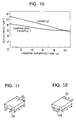
- the produced article was encased in a case 15 made of modified polyamide (Trade Name: ARLEN) made by Mitsui Petrochemical Co., Ltd. and the case 15 are fixed to each other with epoxy system adhesives.
- the outer appearance is shown in Figs. 11 and 12.
- a toroidal choke coil 11 (TM coil 6 ⁇ H-10A) having the same rated capacitance was produced as shown in Figs. 5 and 6.
- Example 2 a surface (one sided) of a Fe-based amorphous magnetic alloy thin strip (Trade Name: "Metglas 2605S-2", composition: Fe 78 Si 9 B 13 , thickness: 20 ⁇ m, width: 5 mm) made by US Allide-Signal Inc. was wound to a magnetic core 12 having an outside diameter of 21.5 mm and an inside diameter of 12.0 mm. The winding was subjected to a heat treatment and was received in the resin case 15. Thereafter, two lead lines 16 each having a diameter of 1.1 mm were wound in parallel by eight turns about a circumferential direction of the case 15 made of resin. As a result, a toroidal choke 11 having an outside diameter (l) of 27 mm and a height (h) of 12 mm was obtained.
- a Fe-based amorphous magnetic alloy thin strip (Trade Name: "Metglas 2605S-2", composition: Fe 78 Si 9 B 13 , thickness: 20 ⁇ m, width: 5 mm) made by US Allide-S
- the foot print was small in comparison with the conventional article, and the actual height was about half of the conventional article.
Landscapes
- Engineering & Computer Science (AREA)
- Power Engineering (AREA)
- Microelectronics & Electronic Packaging (AREA)
- Coils Or Transformers For Communication (AREA)
- Soft Magnetic Materials (AREA)
Claims (6)
- Induktionselement, das einen magnetischen Kern (2), der einen hohlen Abschnitt in der Nähe eines Zentrums aufweist, und eine Leitung (1), die durch den hohlen Abschnitt des magnetischen Kerns läuft, aufweist, dadurch gekennzeichnet, daß der magnetische Kern aus einer Fe-basierten nanokristallinen Legierung gemacht ist,eine relative Permeabilität µ des magnetischen Kerns in dem Bereich von 100 bis 2000 liegt, unddas Induktionselement die folgenden Formeln erfüllt:
- Induktionselement nach Anspruch 1, bei dem der magnetische Kern durch Wickeln eines dünnen Streifens (3) einer magnetischen Legierung ausgebildet ist.
- Induktionselement nach Anspruch 2, bei dem die Leitung verwendet wird als ein Kernteil und der dünne Streifen einer magnetischen Legierung direkt auf das Kernteil gewickelt ist.
- Induktionselement nach Anspruch 1, bei dem der magnetische Kern durch Laminieren von Lagen einer magnetischen Legierung ausgebildet ist.
- Zusammengebaute Einheit, bei der eine Mehrzahl von Induktionselementen, von denen jedes entsprechend einem der Ansprüche 1 bis 4 ist, parallel angeordnet ist, wobei jeder magnetischer Kernabschnitt durch ein Harz zur Ausbildung einer Verpackung versiegelt ist und die Leitung jedes Induktionselements aus einer Seitenwand der Verpackung vorsteht.
- Zusammengebaute Einheit nach Anspruch 5, bei der ein Gehäuse, das aus einem nicht-magnetischen Material gemacht ist, für die Verpackung anstelle der Harzversiegelung verwendet wird.
Applications Claiming Priority (6)
| Application Number | Priority Date | Filing Date | Title |
|---|---|---|---|
| JP295700/93 | 1993-11-25 | ||
| JP29570093 | 1993-11-25 | ||
| JP29570093 | 1993-11-25 | ||
| JP313980/94 | 1994-11-24 | ||
| JP31398094 | 1994-11-24 | ||
| JP6313980A JPH07201610A (ja) | 1993-11-25 | 1994-11-24 | インダクタンス素子およびこれを用いた集合素子 |
Publications (2)
| Publication Number | Publication Date |
|---|---|
| EP0655754A1 EP0655754A1 (de) | 1995-05-31 |
| EP0655754B1 true EP0655754B1 (de) | 2000-09-13 |
Family
ID=26560384
Family Applications (1)
| Application Number | Title | Priority Date | Filing Date |
|---|---|---|---|
| EP94308728A Expired - Lifetime EP0655754B1 (de) | 1993-11-25 | 1994-11-25 | Induktives Bauelement |
Country Status (7)
| Country | Link |
|---|---|
| US (1) | US5815060A (de) |
| EP (1) | EP0655754B1 (de) |
| JP (1) | JPH07201610A (de) |
| KR (1) | KR0161557B1 (de) |
| CN (1) | CN1080445C (de) |
| DE (1) | DE69425867T2 (de) |
| TW (1) | TW338831B (de) |
Families Citing this family (34)
| Publication number | Priority date | Publication date | Assignee | Title |
|---|---|---|---|---|
| US6014111A (en) * | 1997-06-05 | 2000-01-11 | Megapulse, Inc. | Ferrite crossed-loop antenna of optimal geometry and construction and method of forming same |
| JP4308426B2 (ja) | 1997-10-14 | 2009-08-05 | バクームシユメルツエ、ゲゼルシヤフト、ミツト、ベシユレンクテル、ハフツング | 無線障害抑制チョークコイル |
| DE19942815C2 (de) * | 1999-09-08 | 2001-06-28 | Daimler Chrysler Ag | Vorrichtung zur Ansteuerung eines Airbags |
| EP1381061B1 (de) * | 2001-03-30 | 2011-08-24 | Nippon Chemi-Con Corporation | Induktivitätselement und gehäuse |
| JP2002299124A (ja) * | 2001-03-30 | 2002-10-11 | Nippon Chemicon Corp | インダクタンス素子 |
| US6741153B1 (en) * | 2002-12-30 | 2004-05-25 | Industrial Technology Research Institute | Flat high-voltage impulse transformer |
| JP4039341B2 (ja) * | 2003-08-18 | 2008-01-30 | 松下電器産業株式会社 | マルチフェーズ回路 |
| JP2006120887A (ja) * | 2004-10-22 | 2006-05-11 | Sumida Corporation | 磁性素子 |
| US7751205B2 (en) * | 2006-07-10 | 2010-07-06 | Ibiden Co., Ltd. | Package board integrated with power supply |
| US7791445B2 (en) | 2006-09-12 | 2010-09-07 | Cooper Technologies Company | Low profile layered coil and cores for magnetic components |
| US8378777B2 (en) * | 2008-07-29 | 2013-02-19 | Cooper Technologies Company | Magnetic electrical device |
| US8941457B2 (en) | 2006-09-12 | 2015-01-27 | Cooper Technologies Company | Miniature power inductor and methods of manufacture |
| US9589716B2 (en) | 2006-09-12 | 2017-03-07 | Cooper Technologies Company | Laminated magnetic component and manufacture with soft magnetic powder polymer composite sheets |
| US8466764B2 (en) | 2006-09-12 | 2013-06-18 | Cooper Technologies Company | Low profile layered coil and cores for magnetic components |
| US8310332B2 (en) | 2008-10-08 | 2012-11-13 | Cooper Technologies Company | High current amorphous powder core inductor |
| JP5316921B2 (ja) * | 2007-03-16 | 2013-10-16 | 日立金属株式会社 | Fe基軟磁性合金、およびこれを用いた磁性部品 |
| JP5316920B2 (ja) * | 2007-03-16 | 2013-10-16 | 日立金属株式会社 | 軟磁性合金、アモルファス相を主相とする合金薄帯、および磁性部品 |
| US7936244B2 (en) * | 2008-05-02 | 2011-05-03 | Vishay Dale Electronics, Inc. | Highly coupled inductor |
| US10134525B2 (en) * | 2008-05-16 | 2018-11-20 | Hitachi Metals Ltd. | Dust core and choke |
| US8659379B2 (en) | 2008-07-11 | 2014-02-25 | Cooper Technologies Company | Magnetic components and methods of manufacturing the same |
| US9859043B2 (en) | 2008-07-11 | 2018-01-02 | Cooper Technologies Company | Magnetic components and methods of manufacturing the same |
| US8279037B2 (en) | 2008-07-11 | 2012-10-02 | Cooper Technologies Company | Magnetic components and methods of manufacturing the same |
| US9558881B2 (en) | 2008-07-11 | 2017-01-31 | Cooper Technologies Company | High current power inductor |
| JP2010062409A (ja) * | 2008-09-05 | 2010-03-18 | Panasonic Corp | インダクター部品 |
| JP5560078B2 (ja) * | 2010-03-29 | 2014-07-23 | 株式会社ダイヘン | 電源装置 |
| JP2015135870A (ja) * | 2014-01-16 | 2015-07-27 | 富士通株式会社 | インダクタ装置及びインダクタ装置の製造方法 |
| CN103943308A (zh) * | 2014-04-22 | 2014-07-23 | 安徽众恒复合材料科技有限公司 | 一种扼流圈 |
| DE102014007780B4 (de) * | 2014-05-21 | 2026-02-05 | Audi Ag | Energiespeicheranordnung für ein Kraftfahrzeug und Kraftfahrzeug |
| JPWO2018179326A1 (ja) * | 2017-03-31 | 2019-12-12 | 三菱電機株式会社 | ノイズフィルタおよび電力変換装置 |
| WO2020111137A1 (ja) * | 2018-11-28 | 2020-06-04 | 日本ケミコン株式会社 | 電子部品およびその製造方法 |
| JP7298139B2 (ja) * | 2018-11-28 | 2023-06-27 | 日本ケミコン株式会社 | 電子部品およびその製造方法 |
| JP7196566B2 (ja) * | 2018-11-28 | 2022-12-27 | 日本ケミコン株式会社 | 電子部品およびその製造方法 |
| JP7349904B2 (ja) * | 2019-12-26 | 2023-09-25 | 株式会社藤商事 | 遊技機 |
| US12142407B2 (en) * | 2021-02-26 | 2024-11-12 | Infineon Technologies Austria Ag | Inductor devices and stacked power supply topologies |
Family Cites Families (10)
| Publication number | Priority date | Publication date | Assignee | Title |
|---|---|---|---|---|
| US1857215A (en) * | 1930-03-05 | 1932-05-10 | Gen Electric | Electrical induction apparatus |
| JPS5696812A (en) * | 1979-12-28 | 1981-08-05 | Matsushita Electric Works Ltd | Inductance device |
| US4637843A (en) * | 1982-05-06 | 1987-01-20 | Tdk Corporation | Core of a noise filter comprised of an amorphous alloy |
| US4803777A (en) * | 1984-08-07 | 1989-02-14 | Masayuki Nakagawa | Method of manufacturing an electric component with a lead wire secured in a through hole |
| US5062197A (en) * | 1988-12-27 | 1991-11-05 | General Electric Company | Dual-permeability core structure for use in high-frequency magnetic components |
| US4904972A (en) * | 1989-06-28 | 1990-02-27 | Hitachi, Ltd. | Gas-insulated stationary induction electrical apparatus |
| JPH04217307A (ja) * | 1990-12-18 | 1992-08-07 | Mitsubishi Electric Corp | インダクタ |
| US5200730A (en) * | 1991-10-18 | 1993-04-06 | Ferrishield, Inc. | Premolded suppressor sleeve |
| US5243308A (en) * | 1992-04-03 | 1993-09-07 | Digital Equipment Corporation | Combined differential-mode and common-mode noise filter |
| US5455552A (en) * | 1994-05-03 | 1995-10-03 | Steward, Inc. | Ferrite common mode choke adapted for circuit board mounting |
-
1994
- 1994-11-24 JP JP6313980A patent/JPH07201610A/ja active Pending
- 1994-11-25 EP EP94308728A patent/EP0655754B1/de not_active Expired - Lifetime
- 1994-11-25 DE DE69425867T patent/DE69425867T2/de not_active Expired - Lifetime
- 1994-11-25 US US08/348,895 patent/US5815060A/en not_active Expired - Lifetime
- 1994-11-25 CN CN94118448A patent/CN1080445C/zh not_active Expired - Lifetime
- 1994-11-25 TW TW083110983A patent/TW338831B/zh not_active IP Right Cessation
- 1994-11-25 KR KR1019940031180A patent/KR0161557B1/ko not_active Expired - Fee Related
Also Published As
| Publication number | Publication date |
|---|---|
| EP0655754A1 (de) | 1995-05-31 |
| DE69425867D1 (de) | 2000-10-19 |
| DE69425867T2 (de) | 2001-02-22 |
| KR0161557B1 (ko) | 1999-01-15 |
| JPH07201610A (ja) | 1995-08-04 |
| TW338831B (en) | 1998-08-21 |
| KR950015416A (ko) | 1995-06-16 |
| CN1080445C (zh) | 2002-03-06 |
| US5815060A (en) | 1998-09-29 |
| CN1108790A (zh) | 1995-09-20 |
Similar Documents
| Publication | Publication Date | Title |
|---|---|---|
| EP0655754B1 (de) | Induktives Bauelement | |
| US5481792A (en) | Inductor winding method | |
| EP0299498B1 (de) | Magnetkern und Verfahren zur Herstellung | |
| US20040135660A1 (en) | Low profile high current multiple gap inductor assembly | |
| JP5175844B2 (ja) | インダクタンス素子とその製造方法、およびそれを用いたスイッチング電源 | |
| WO2004042754A1 (en) | Bulk amorphous metal inductive device | |
| JPWO2008132810A1 (ja) | インダクタンス素子とその製造方法、およびそれを用いたスイッチング電源 | |
| EP0655753B1 (de) | Aktiver Filter und seine Benutzung in einer Stromversorgungseinrichtung | |
| EP0306041B1 (de) | Störschutzanordnung | |
| CA2136684C (en) | Inductance element | |
| JPH11176653A (ja) | 磁心とそれを用いた磁性部品 | |
| JP2851268B2 (ja) | ノイズ低減方法 | |
| JP2804029B2 (ja) | ノイズ低減素子 | |
| US6480084B1 (en) | Inductance element and manufacturing method thereof, and snubber using thereof | |
| WO1999003116A1 (fr) | Bobine | |
| JP2000091142A (ja) | リード付き磁性部品及びそれを用いたノイズ低減回路 | |
| US4745536A (en) | Reactor for circuit containing semiconductor device | |
| JP2009071237A (ja) | インダクタタンス素子、その製造方法および電子機器 | |
| JP3421253B2 (ja) | アモルファス巻鉄心変圧器 | |
| JP2807225B2 (ja) | ノイズ低減素子 | |
| JPH06101412B2 (ja) | インダクタ− | |
| JP2002093642A (ja) | インダクタンス素子、その製造方法、およびインダクタンス素子を用いたスナバー回路 | |
| JPH0794328A (ja) | ユニットトランスおよびそれを用いたシステムトランス | |
| JPH02172208A (ja) | インダクタ及びその製造方法 | |
| JP2002252125A (ja) | 磁気素子およびそれを用いたスナバー回路 |
Legal Events
| Date | Code | Title | Description |
|---|---|---|---|
| PUAI | Public reference made under article 153(3) epc to a published international application that has entered the european phase |
Free format text: ORIGINAL CODE: 0009012 |
|
| AK | Designated contracting states |
Kind code of ref document: A1 Designated state(s): DE FR GB IT NL |
|
| 17P | Request for examination filed |
Effective date: 19951123 |
|
| 17Q | First examination report despatched |
Effective date: 19970509 |
|
| RAP1 | Party data changed (applicant data changed or rights of an application transferred) |
Owner name: MITSUI CHEMICALS, INC. |
|
| RAP1 | Party data changed (applicant data changed or rights of an application transferred) |
Owner name: NIPPON CHEMI-CON CORPORATION |
|
| GRAG | Despatch of communication of intention to grant |
Free format text: ORIGINAL CODE: EPIDOS AGRA |
|
| GRAH | Despatch of communication of intention to grant a patent |
Free format text: ORIGINAL CODE: EPIDOS IGRA |
|
| GRAH | Despatch of communication of intention to grant a patent |
Free format text: ORIGINAL CODE: EPIDOS IGRA |
|
| GRAA | (expected) grant |
Free format text: ORIGINAL CODE: 0009210 |
|
| AK | Designated contracting states |
Kind code of ref document: B1 Designated state(s): DE FR GB IT NL |
|
| ITF | It: translation for a ep patent filed | ||
| REF | Corresponds to: |
Ref document number: 69425867 Country of ref document: DE Date of ref document: 20001019 |
|
| ET | Fr: translation filed | ||
| PLBE | No opposition filed within time limit |
Free format text: ORIGINAL CODE: 0009261 |
|
| STAA | Information on the status of an ep patent application or granted ep patent |
Free format text: STATUS: NO OPPOSITION FILED WITHIN TIME LIMIT |
|
| 26N | No opposition filed | ||
| REG | Reference to a national code |
Ref country code: GB Ref legal event code: IF02 |
|
| PGFP | Annual fee paid to national office [announced via postgrant information from national office to epo] |
Ref country code: FR Payment date: 20021108 Year of fee payment: 9 |
|
| PGFP | Annual fee paid to national office [announced via postgrant information from national office to epo] |
Ref country code: GB Payment date: 20021120 Year of fee payment: 9 |
|
| PGFP | Annual fee paid to national office [announced via postgrant information from national office to epo] |
Ref country code: NL Payment date: 20021129 Year of fee payment: 9 |
|
| PG25 | Lapsed in a contracting state [announced via postgrant information from national office to epo] |
Ref country code: GB Free format text: LAPSE BECAUSE OF NON-PAYMENT OF DUE FEES Effective date: 20031125 |
|
| PG25 | Lapsed in a contracting state [announced via postgrant information from national office to epo] |
Ref country code: NL Free format text: LAPSE BECAUSE OF NON-PAYMENT OF DUE FEES Effective date: 20040601 |
|
| GBPC | Gb: european patent ceased through non-payment of renewal fee |
Effective date: 20031125 |
|
| PG25 | Lapsed in a contracting state [announced via postgrant information from national office to epo] |
Ref country code: FR Free format text: LAPSE BECAUSE OF NON-PAYMENT OF DUE FEES Effective date: 20040730 |
|
| NLV4 | Nl: lapsed or anulled due to non-payment of the annual fee |
Effective date: 20040601 |
|
| REG | Reference to a national code |
Ref country code: FR Ref legal event code: ST |
|
| PG25 | Lapsed in a contracting state [announced via postgrant information from national office to epo] |
Ref country code: IT Free format text: LAPSE BECAUSE OF NON-PAYMENT OF DUE FEES;WARNING: LAPSES OF ITALIAN PATENTS WITH EFFECTIVE DATE BEFORE 2007 MAY HAVE OCCURRED AT ANY TIME BEFORE 2007. THE CORRECT EFFECTIVE DATE MAY BE DIFFERENT FROM THE ONE RECORDED. Effective date: 20051125 |
|
| PGFP | Annual fee paid to national office [announced via postgrant information from national office to epo] |
Ref country code: DE Payment date: 20131120 Year of fee payment: 20 |
|
| REG | Reference to a national code |
Ref country code: DE Ref legal event code: R071 Ref document number: 69425867 Country of ref document: DE |