EP0652460B1 - Anzeigevorrichtung mit Flüssigkristallen - Google Patents
Anzeigevorrichtung mit Flüssigkristallen Download PDFInfo
- Publication number
- EP0652460B1 EP0652460B1 EP94117140A EP94117140A EP0652460B1 EP 0652460 B1 EP0652460 B1 EP 0652460B1 EP 94117140 A EP94117140 A EP 94117140A EP 94117140 A EP94117140 A EP 94117140A EP 0652460 B1 EP0652460 B1 EP 0652460B1
- Authority
- EP
- European Patent Office
- Prior art keywords
- electrodes
- display
- counter
- substrate
- electrode
- Prior art date
- Legal status (The legal status is an assumption and is not a legal conclusion. Google has not performed a legal analysis and makes no representation as to the accuracy of the status listed.)
- Expired - Lifetime
Links
Images


Classifications
-
- G—PHYSICS
- G02—OPTICS
- G02F—OPTICAL DEVICES OR ARRANGEMENTS FOR THE CONTROL OF LIGHT BY MODIFICATION OF THE OPTICAL PROPERTIES OF THE MEDIA OF THE ELEMENTS INVOLVED THEREIN; NON-LINEAR OPTICS; FREQUENCY-CHANGING OF LIGHT; OPTICAL LOGIC ELEMENTS; OPTICAL ANALOGUE/DIGITAL CONVERTERS
- G02F1/00—Devices or arrangements for the control of the intensity, colour, phase, polarisation or direction of light arriving from an independent light source, e.g. switching, gating or modulating; Non-linear optics
- G02F1/01—Devices or arrangements for the control of the intensity, colour, phase, polarisation or direction of light arriving from an independent light source, e.g. switching, gating or modulating; Non-linear optics for the control of the intensity, phase, polarisation or colour
- G02F1/13—Devices or arrangements for the control of the intensity, colour, phase, polarisation or direction of light arriving from an independent light source, e.g. switching, gating or modulating; Non-linear optics for the control of the intensity, phase, polarisation or colour based on liquid crystals, e.g. single liquid crystal display cells
- G02F1/133—Constructional arrangements; Operation of liquid crystal cells; Circuit arrangements
- G02F1/1333—Constructional arrangements; Manufacturing methods
- G02F1/1343—Electrodes
- G02F1/134309—Electrodes characterised by their geometrical arrangement
- G02F1/134327—Segmented, e.g. alpha numeric display
-
- G—PHYSICS
- G02—OPTICS
- G02F—OPTICAL DEVICES OR ARRANGEMENTS FOR THE CONTROL OF LIGHT BY MODIFICATION OF THE OPTICAL PROPERTIES OF THE MEDIA OF THE ELEMENTS INVOLVED THEREIN; NON-LINEAR OPTICS; FREQUENCY-CHANGING OF LIGHT; OPTICAL LOGIC ELEMENTS; OPTICAL ANALOGUE/DIGITAL CONVERTERS
- G02F1/00—Devices or arrangements for the control of the intensity, colour, phase, polarisation or direction of light arriving from an independent light source, e.g. switching, gating or modulating; Non-linear optics
- G02F1/01—Devices or arrangements for the control of the intensity, colour, phase, polarisation or direction of light arriving from an independent light source, e.g. switching, gating or modulating; Non-linear optics for the control of the intensity, phase, polarisation or colour
- G02F1/13—Devices or arrangements for the control of the intensity, colour, phase, polarisation or direction of light arriving from an independent light source, e.g. switching, gating or modulating; Non-linear optics for the control of the intensity, phase, polarisation or colour based on liquid crystals, e.g. single liquid crystal display cells
- G02F1/133—Constructional arrangements; Operation of liquid crystal cells; Circuit arrangements
- G02F1/1333—Constructional arrangements; Manufacturing methods
- G02F1/1343—Electrodes
- G02F1/13439—Electrodes characterised by their electrical, optical, physical properties; materials therefor; method of making
Definitions
- the present invention relates to a device liquid crystal display and more particularly such a device for displaying symbols fixed display at the same time as symbols changing display.
- Current crystal displays liquids have a relatively simple structure. They are formed essentially by two spaced substrates, of which at least one is transparent, a crystal compound liquids enclosed between substrates and electrodes conductive provided on the opposite faces opposite substrates and arranged to represent the different display symbols.
- a voltage source is climb to apply a field between games electrodes inside the space formed between the substrates. The application of the field acts on the compound formed by liquid crystals and thereby changes its transmission or reflection characteristics of the light.
- liquid crystal displays have been used in many applications, especially in pocket calculators, wristwatches, measuring instruments, receivers people and various other instruments e.
- the advantage of such display devices lies in that they can be directly ordered by integrated circuit chips and what they can display various symbols in a small space.
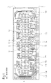
- Figures 1 and 2 are plan views respectively from the front face of a first substrate 1 and of the rear face of a second substrate 2 of a liquid crystal display device of a type known. These two substrates or plates 1 and 2 are each fitted with a set of electrodes. The electrodes on each plate are subdivided into those that form symbols fixed and those divided into groups of seven segments in the shape of "8".
- All electrodes are arranged inside a sealing frame 3 which forms, with the two plates 1 and 2, a cell inside which is enclosed a layer of liquid crystals 4.
- Terminals 1.3 are deposited on the front plate 1, outside the frame 3, conductive tracks 1.4 lead from these terminals to electrodes 1.1 and 1.2.
- Certain terminals 1.3 designated by the references 1.31, 1.32 and 1.33, are connected to the electrodes on plate 2 by via connection bridges (not shown A, B and C) which connect the two substrates to each other at frame level 3.
- the electrodes of plate 2 are subdivided into three parts, to which are respectively connected the three terminals 1.31, 1.32 and 1.33.
- the first part 5 brings together all the electrodes 2.1 forming symbols fixed and all the electrodes 2.2 forming a first segment of the seven segments in the shape of "8".
- the second part 6 brings together all the 2.2 electrodes forming second, third and fourth segments of the seven "8" shaped segments.
- the third part 7 brings together all 2.2 electrodes forming fifth, sixth and seventh segments of the seven segments in the shape of "8". Parts 5, 6 and 7 are respectively linked to terminals 1.33, 1.31 and 1.32.
- a voltage is applied between electrode 7 and a terminal 1.34, which is indirectly connected to the electrodes 1.1 having the form of the word "ON".
- US Patent 4,522,691 describes a device display having multiple display electrodes formed in parallel on the surface of a first substrate and several counter-electrodes formed in parallel on the surface of a second substrate spaced from the first substrate.
- the display electrodes and counter electrodes are oriented so that their directions intersect at right angle, thus forming a matrix of elements each item can be selected by selectively applying a switching voltage between one of the display electrodes and one of the counter electrodes.
- This device constitutes a display matrix, which can display changing symbols according to a known multiplexing system, thus offering more great flexibility in the type of symbols that can be displayed, than that achievable with a seven display segments.
- an object of the invention is to achieve a liquid crystal display device which improves prior art or which overcomes its disadvantages.
- Another object of the invention is to provide a advanced liquid crystal display device allowing the display of changing symbols as well than fixed symbols.
- the subject of the invention is therefore a device display as defined in claim 1.
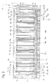
- first front substrate 10 and a second rear substrate 11 of a first embodiment of a device liquid crystal display according to this invention are preferably made of glass or plastic such as MYLAR ®, a polycarbonate or Plexiglass ®. They are each provided with electrodes at least partially superimposed so as to allow the display of the various symbols when a switching voltage is applied selectively between them.
- Display electrodes for forming fixed symbols are formed on the substrate 11. These electrodes are designated by the references 12 to 48 and each have the form of a letter ("O", "F”, “F”, etc.) or of another fixed symbol.
- second display electrodes On the same face of this substrate 11, is formed a set of elongated second display electrodes intended to form changing symbols. These electrodes are designated by the references 50 to 56 and juxtaposed on the surface of the substrate 11, according to a first executive management. Preferably, these second electrodes are generally straight and extend over substantially the entire length of the substrate surface 11.
- All electrodes 12 to 30 are connected together to a connection bridge 57 by a conductive track 57a, while all the electrodes 31 to 48 are connected together at a bridge and connection 58 by a track conductor 58a.
- the electrodes 50 to 56 are respectively connected to connection bridges 59 to 65 by conductive tracks 59a to 65a.
- These electrodes are designated by the references 70 to 129 and juxtaposed on the surface of the substrate 10 in a second direction general perpendicular to the first general direction.
- the counter electrodes are generally straight and extend over substantially the width entire surface of the substrate 10.
- All the electrodes 70 to 129 are provided for inside a sealing frame 130 which forms, with the two substrates 10 and 11, a cell inside which is enclosed by a layer of liquid crystals.
- of the terminals 140 to 199 are arranged on the substrate 10, at outside the frame 130, and respectively connected to the electrodes 70 to 129.
- terminals 200 to 208 are also arranged on the substrate 10 to ensure the connection with the electrodes on the substrate 11, respectively via the connection bridges 58, 65, 64, 57, 59, 60, 61, 62 and 63.
- the electrodes 70 to 129 and 50 to 56 of the device liquid crystal display shown in Figures 3 and 4 form a matrix display of elements display, a combination of which can be selected to allow display of various symbols changing.
- counter-electrodes 70 to 129 are superimposed on display electrodes 12 to 48 so as to function as a counter electrode for cooperate with them so that we can do without counter electrodes which would be associated exclusively with these electrodes 12 to 48.
- the counter-electrodes formed on the substrate 10 can be subdivided into several groups, each of which, for example that formed by the electrodes 70 to 74, is intended to display a particular display symbol. In order to improve the readability of the symbols displayed, these electrode groups can be spaced laterally relative to each other. In case at least part of one of the display electrodes 12 to 48 is superimposed on the space between two groups of electrodes, the set of counter-electrodes of the substrate 10 can further comprise at least one partial electrode located in this space to function as a part counter-electrode cooperating with the electrode display 12 to 48 concerned.
- partial counter-electrodes are designated by the references 74a, 74b, 79a, 79b, 89a, 89b, 94a, 99a, 99b, 104a, 109a, 109b, 119a and 124a.
- Each of these counter electrodes partial can be connected by a track conductive (not shown) to at least one of the counter electrodes adjacent.
- the display device illustrated in Figures 3 and 4 may further include a display window arranged in a frame which is designated by the reference 220.
- This frame 220 allows the reading of the central part substrates 10 and 11, while hiding from view the outer parts of substrates 10 and 11. This results that the overlays of the conductive tracks and electrodes on both substrates, which otherwise would create readable lines in the presence of tension switch, are hidden behind the frame 220.
- each other conductive tracks 57a and 58a on the substrate 11 can extend into the spaces between these groups electrodes so you can get close to the electrodes display 12 to 48.
- a portion 57b of the conductive track 57a which extends in the space separating the electrode groups 110 to 114 and 115 to 119, (see also Figure 3).
- the narrow portion 57c of the runway conductor 57a which is superimposed on the counter electrode 114 may be of minimum length, the dimensions of the rest of the conductive track 57a may be maximum.
- the conductive track 57a can be produced with more reliability without risk of breakage. If one partial electrode, for example the partial electrode 79a, is located between two groups of counter-electrodes, the part 57d of the conductive track 57a whose dimensions are maximum can extend into the separation space to the edge of the partial electrode 79a before its width is not reduced in part 57e.
- the display electrodes intended to display fixed symbols are located on the lateral sides of the display electrode assembly intended to display changing symbols.
- FIGS. 3 and 4 we have shown plan views of a first front substrate 250 and a second rear substrate 251 on which display electrodes for displaying fixed symbols are located only on one of the two side sides of the display electrode assembly intended to display changing symbols.
- the substrate 250 has on one of its faces first display electrodes intended to form fixed symbols such as electrodes 31 to 48, shaped letter ("N", “E”, “W”, etc.) or other symbols fixed, and second display electrodes designated by references 252 to 258.
- these seconds display electrodes 252 to 257 each have a shape corresponding to at least one group of several counter-electrodes intended to display the fixed symbols.
- These counter electrodes are formed on the substrate 251.
- all the electrodes 252 to 258 are connected together to the bridge connection 57 by the conductive track 57a.
- all the electrodes 31 to 48 are connected together to the connection bridge 58 by the conductive track 58a and the electrodes 50 to 56 are respectively connected to the connection bridges 59 to 65 via conductive tracks 59a at 65a.
- one of the faces of the substrate 251 has a set of elongated counter electrodes intended to form changing symbols in combination with electrodes 50 to 56.
- These counter electrodes are designated by the references 300 to 359 and are juxtaposed on the face of the substrate 251 in a second direction general perpendicular to the first general direction.
- these counter-electrodes are generally straight and extend only over part of the width of the substrate surface 250.
- terminals 140 to 199 are respectively connected to electrodes 300 to 359, while others terminals 200 to 208 are deposited on the substrate 251 for ensuring the connection with the electrodes of the substrate 250, respectively via connection bridges 58, 65, 64, 57, 59, 60, 61, 62 and 63.
- Counter electrodes for forming symbols fixed are formed on the same face of the substrate 251. These counter-electrodes are designated by the references 360 to 378 and each has the form of a letter ("O", “F”, “F”, etc.) or another fixed symbol. Preferably, they are all located on the same lateral side of the set of display electrodes 50 to 56.
- Some of the counter electrodes 300 to 359 are superimposed on display electrodes 31 to 48 which are found on the opposite side of the assembly display electrodes 50 to 56 to operate respectively as a counter electrode for these.
- Each of the counter electrodes 360 to 378 can be connected either directly or indirectly to one of the counter electrodes 300 to 359. Indeed, as shown in FIG. 6, one or more conductive tracks 305a, 314a, 323a, 335a and 346a can be formed on the surface of substrate 251 to ensure a connection between the counter electrodes 360 to 378 and some of the counter electrodes 300 to 359.
- the conductive tracks 305a, 314a, 323a, 335a and 346a are respectively connected to the counter electrodes 305, 314, 323, 335 and 346.
- the counter electrodes 360 to 378 are subdivided into groups of fixed symbols in order to display, for example, words like "OFF", "TIME”, etc. in case a switching voltage is applied to both all counter electrodes in a selected group.
- all the counter electrodes of a group for example example the counter electrodes 361 to 363, can be connected to the same conductive track 305a, i.e. directly, either through another electrode in the group.
- the counter electrodes formed on the substrate 251 can also be subdivided into several groups each of which, for example electrodes 305 to 309, is intended to display a particular display symbol. These groups of electrodes can be separated laterally relative to each other. In the event that part of at least one of the display electrodes 31 to 48 is superimposed on the space separating two groups of electrodes, the set of counter-electrodes on the substrate 251 can further comprise at least one partial electrode located in this space so that it can function as part of a counter electrode for one of the display electrodes 31 to 48.
- partial counter electrodes are designated by the references 74a, 74b, 79a, 79b, 89a, 89b, 94a, 99a, 99b, 104a, 109a, 109b, 119a and 124a.
- Each of these electrodes partial can be connected by a conductive track (not shown) at least one of the counter electrodes adjacent.
- the rear substrate and the front substrate can be substituted for each other.
- the display electrodes and the counter electrodes can be substituted for each other, without going outside the framework of the invention.
Claims (3)
- Anzeigevorrichtung, die umfaßt:dadurch gekennzeichnet, daß wenigstens zwei Gegenelektroden der Gesamtheit von Gegenelektroden (70-129; 300-359) der wenigstens einen ersten Anzeigeelektrode (31-48) überlagert sind, um ein festes Anzeigesymbol bei Vorhandensein einer zwischen ihnen angelegten Umschaltspannung zu erzeugen, wobei der Abstand, der die einen von den anderen benachbarten Gegenelektroden der Gesamtheit von Gegenelektroden (70-129; 300-359), die der wenigstens einen ersten Anzeigeelektrode (31-48) überlagert sind, trennt, deutlich kleiner als die Breite der ersten Anzeigeelektrode (31-48) ist und daß die Gegenelektroden (70-129; 300-359) in jedem der Bereiche, die durch die ersten (31-48) und zweiten (50-56) Anzeigeelektroden definiert sind, zueinander parallel sind.ein erstes Substrat (11; 250) und ein zweites Substrat (10; 251), die voneinander beabstandet sind und einander gegenüberliegen,eine Schicht aus Flüssigkristallen, die zwischen zwei optisch wahrnehmbaren Zuständen umschaltbar sind, wobei diese Schicht in den Raum eingeschlossen ist, der zwischen dem ersten und dem zweiten Substrat (10, 11; 250, 251) begrenzt ist,wenigstens eine erste Anzeigeelektrode (31-48), die die Form eines festen Symbols hat, die auf der Fläche des ersten Substrats (11; 250) gegenüber dem zweiten Substrat (10; 251) ausgebildet ist,eine Gesamtheit zweiter langgestreckter Anzeigeelektroden (50-56), die auf der Fläche des ersten Substrats (11; 250) gegenüber dem zweiten Substrat (10; 251) ausgebildet sind und auf dem ersten Substrat (11; 250) in einer ersten allgemeinen Richtung im wesentlichen über die gesamte Länge des ersten Substrats (11; 250) nebeneinander angeordnet sind, undeine Gesamtheit langgestreckter Gegenelektroden (70-129; 300-359), die auf der Fläche des zweiten Substrats (10; 251) gegenüber dem ersten Substrat (11; 250) ausgebildet sind und auf dem zweiten Substrat (10; 251) in einer zweiten allgemeinen Richtung, die zur ersten allgemeinen Richtung senkrecht ist, im wesentlichen über die gesamte Breite des zweiten Substrats (10; 251) nebeneinander angeordnet und den zweiten Anzeigeelektroden (50-56) überlagert sind, um eine matrixförmige Anzeige aus Anzeigeelementen zu erzeugen, die dazu bestimmt sind, wechselnde Anzeigesymbole zu erzeugen, welche durch wahlweises Anlegen einer Umschaltspannung zwischen ihnen wechselnde Anzeigesymbole bilden können, wobei die Gegenelektroden (70-129; 300-359) außerdem der oder jeder ersten Anzeigeelektrode (31-48) überlagert sind,
- Anzeigevorrichtung nach Anspruch 1, dadurch gekennzeichnet, daß die Gegenelektroden (70-129; 300-359) in mehreren beabstandeten Gruppen verteilt sind, wovon jede dazu bestimmt ist, ein einzelnes wechselndes Anzeigesymbol anzuzeigen, wobei die Gesamtheit von zweiten Gegenelektroden (70-129; 300-359) außerdem wenigstens eine zweite partielle Gegenelektrode umfaßt, die mit einer benachbarten zweiten Gegenelektrode verbunden ist, wobei sich die zweite partielle Gegenelektrode in dem Raum zwischen benachbarten Gruppen von zweiten Gegenelektroden befindet, wobei die zweite Anzeigegegenelektrode somit einen Teil der ersten Gegenelektrode bildet.
- Anzeigevorrichtung nach Anspruch 1, dadurch gekennzeichnet, daß sie außerdem umfaßt:wenigstens eine dritte Anzeigeelektrode (12-30), die auf der Fläche des ersten Substrats (11; 250) gegenüber dem zweiten Substrat (10; 251) gebildet ist, wobei die Gegenelektroden der dritten Anzeigeelektrode in der Weise überlagert sind, daß bei Vorhandensein der zwischen ihnen angelegten Umschaltspannung ein festes Anzeigesymbol erzeugt wird, wobei sich die ersten und dritten Anzeigeelektroden (31-48; 12-30) auf den Seiten befinden, die der Gesamtheit von zweiten Anzeigeelektroden (70-129; 300-359) gegenüberliegen.
Applications Claiming Priority (2)
| Application Number | Priority Date | Filing Date | Title |
|---|---|---|---|
| FR9313121 | 1993-11-04 | ||
| FR9313121A FR2712109B1 (fr) | 1993-11-04 | 1993-11-04 | Dispositif d'affichage à cristaux liquides. |
Publications (2)
| Publication Number | Publication Date |
|---|---|
| EP0652460A1 EP0652460A1 (de) | 1995-05-10 |
| EP0652460B1 true EP0652460B1 (de) | 2002-07-03 |
Family
ID=9452500
Family Applications (1)
| Application Number | Title | Priority Date | Filing Date |
|---|---|---|---|
| EP94117140A Expired - Lifetime EP0652460B1 (de) | 1993-11-04 | 1994-10-29 | Anzeigevorrichtung mit Flüssigkristallen |
Country Status (8)
| Country | Link |
|---|---|
| US (1) | US5513027A (de) |
| EP (1) | EP0652460B1 (de) |
| JP (1) | JPH07181914A (de) |
| KR (1) | KR100347988B1 (de) |
| CN (1) | CN1096003C (de) |
| DE (1) | DE69430895T2 (de) |
| FR (1) | FR2712109B1 (de) |
| TW (1) | TW270992B (de) |
Families Citing this family (10)
| Publication number | Priority date | Publication date | Assignee | Title |
|---|---|---|---|---|
| JPH08160443A (ja) * | 1994-12-06 | 1996-06-21 | Nec Corp | Lcd表示装置 |
| GB2321993B (en) * | 1997-02-05 | 2001-02-28 | Nokia Mobile Phones Ltd | Display with icon row |
| US6344838B1 (en) | 1998-04-06 | 2002-02-05 | Em Microelectronic-Marlin Sa | Control device for a liquid crystal display cell |
| DE69827111T2 (de) * | 1998-04-07 | 2006-02-23 | Em Microelectronic-Marin S.A., Marin | Ansteuervorrichtung einer Flüssigkristall-Anzeigezelle |
| JP2000221897A (ja) | 1999-02-01 | 2000-08-11 | Seiko Epson Corp | 表示装置及びこれを用いた電子装置 |
| JP3405972B2 (ja) * | 2000-01-11 | 2003-05-12 | 株式会社東芝 | 液晶表示装置 |
| JP2005010186A (ja) * | 2003-06-16 | 2005-01-13 | Nanox Corp | 液晶表示素子 |
| JP3204586U (ja) | 2012-11-29 | 2016-06-09 | シャークニンジャ オペレーティング エルエルシー | 蒸気式清掃機器 |
| CN109581763B (zh) * | 2019-01-30 | 2021-11-23 | 天马微电子股份有限公司 | 一种显示面板和显示装置 |
| KR102328391B1 (ko) * | 2019-12-19 | 2021-11-18 | 주식회사 포스코 | 단일 금속을 이용한 블랙 컬러 강판 및 그 제조방법 |
Family Cites Families (14)
| Publication number | Priority date | Publication date | Assignee | Title |
|---|---|---|---|---|
| US3781080A (en) * | 1972-11-30 | 1973-12-25 | Gen Electric | Liquid crystal device for generating reticles in optical equipment |
| US3902790A (en) * | 1974-01-14 | 1975-09-02 | Hughes Aircraft Co | Liquid crystal display pattern |
| JPS5234918B2 (de) * | 1974-05-31 | 1977-09-06 | ||
| JPS5488794A (en) * | 1977-12-26 | 1979-07-14 | Seiko Instr & Electronics Ltd | Electro-optical display device |
| JPS559169A (en) * | 1978-07-07 | 1980-01-23 | Citizen Watch Co Ltd | Electronic clock provided with means for matrix display |
| JPS55103589A (en) * | 1979-02-02 | 1980-08-07 | Hitachi Ltd | Liquid crystal display unit |
| JPS5660483A (en) * | 1979-10-24 | 1981-05-25 | Hitachi Ltd | Liquid crystal display unit |
| US4435046A (en) * | 1980-04-08 | 1984-03-06 | Citizen Watch Company Limited | Liquid crystal display device |
| EP0113237B1 (de) * | 1982-12-22 | 1987-11-25 | Seiko Instruments Inc. | Verfahren zum Herstellen eines Mehrfarbenfilters und einer Mehrfarben-Anzeigevorrichtung |
| JPS59123875A (ja) * | 1982-12-28 | 1984-07-17 | セイコーエプソン株式会社 | 液晶表示装置 |
| JPS60107621A (ja) * | 1983-11-16 | 1985-06-13 | Seiko Epson Corp | 液晶表示体 |
| JPS62209416A (ja) * | 1986-03-10 | 1987-09-14 | Nippon Denso Co Ltd | 液晶表示装置 |
| US4834506A (en) * | 1987-07-02 | 1989-05-30 | International Business Machines Corporation | Perceived contrast of liquid crystal displays |
| JPH04174417A (ja) * | 1990-11-07 | 1992-06-22 | Sharp Corp | カラー液晶表示装置 |
-
1993
- 1993-11-04 FR FR9313121A patent/FR2712109B1/fr not_active Expired - Fee Related
-
1994
- 1994-10-28 US US08/331,098 patent/US5513027A/en not_active Expired - Fee Related
- 1994-10-28 TW TW083109982A patent/TW270992B/zh active
- 1994-10-29 EP EP94117140A patent/EP0652460B1/de not_active Expired - Lifetime
- 1994-10-29 DE DE69430895T patent/DE69430895T2/de not_active Expired - Fee Related
- 1994-11-03 KR KR1019940028704A patent/KR100347988B1/ko not_active IP Right Cessation
- 1994-11-03 CN CN94117805A patent/CN1096003C/zh not_active Expired - Fee Related
- 1994-11-04 JP JP6271050A patent/JPH07181914A/ja active Pending
Also Published As
| Publication number | Publication date |
|---|---|
| KR100347988B1 (ko) | 2002-11-30 |
| KR950014929A (ko) | 1995-06-16 |
| TW270992B (de) | 1996-02-21 |
| CN1118492A (zh) | 1996-03-13 |
| DE69430895T2 (de) | 2003-02-27 |
| JPH07181914A (ja) | 1995-07-21 |
| FR2712109A1 (fr) | 1995-05-12 |
| FR2712109B1 (fr) | 1995-12-15 |
| US5513027A (en) | 1996-04-30 |
| EP0652460A1 (de) | 1995-05-10 |
| DE69430895D1 (de) | 2002-08-08 |
| CN1096003C (zh) | 2002-12-11 |
Similar Documents
| Publication | Publication Date | Title |
|---|---|---|
| FR2623649A1 (fr) | Cellule d'affichage a cristal liquide | |
| EP0652460B1 (de) | Anzeigevorrichtung mit Flüssigkristallen | |
| EP0202974B1 (de) | Matrix-Farbbildschirm, seine Herstellung und einen solchen Schirm enthaltendes Gerät | |
| FR2509073A1 (fr) | Dispositif d'affichage miniature a volets | |
| FR2462690A1 (fr) | Systeme d'affichage, en particulier pour vehicules automobiles | |
| FR2461992A1 (fr) | Dispositif d'affichage a cristaux liquides | |
| EP0203005A1 (de) | Dreifarbiger Elektrolumineszenzbildschirm in Matrixform sowie Verfahren zu dessen Herstellung | |
| US7336410B2 (en) | High-definition pixel structure of electrochromic displays and method of producing the same | |
| EP3650957A1 (de) | Gegenstand, der mit einer elektrooptischen anzeigevorrichtung ausgestattet ist | |
| FR2794884A1 (fr) | Afficheur a cristaux liquides | |
| EP1518145B1 (de) | Anzeigezelle, insbesondere flüssigkristall- oder photovoltaische zelle mit mitteln zur verbindung mit einer elektronischen steuerschaltung | |
| EP2721598A1 (de) | Flüssigkristallanzeige mit löschelektroden | |
| FR2739210A1 (fr) | Affichage a cristaux liquides | |
| EP0493178A1 (de) | Matrixfarbanzeigevorrichtung mit Dreieckfarbfilteranordnung | |
| EP3144704A2 (de) | Vorrichtung zur bilderfassung mit integrierter beleuchtung, und herstellungsverfahren dieser vorrichtung | |
| EP0278194B1 (de) | Elektrolumineszenzanzeige mit Speichereffekt, gesteuert durch mehrfache phasenverschobene Auffrischspannungen | |
| EP0734043B1 (de) | Doppel-Gate-Flaches Bildschirm | |
| FR2646269A1 (fr) | Cellule d'affichage electro-optique perfectionnee | |
| EP0007885A1 (de) | Vorrichtung zur selektiven Anzeige aus einer Vielzahl von Informationen und Verfahren zu ihrer Herstellung | |
| CH625630A5 (de) | ||
| FR2752987A1 (fr) | Dispositif d'affichage electro-optique et support flexible pour de tels dispositifs servant a l'alimentation de ces dispositifs | |
| CH639791A5 (fr) | Cellule d'affichage electro-optique passif. | |
| EP0057805B1 (de) | Eine Punktmatrix verwendende optoelektronische Anzeige | |
| EP1324110B1 (de) | Flüssigkristallzelle mit mindestens zwei Beugungsgittern insbesondere für einen optischen Strahlteiler | |
| CH715286B1 (fr) | Objet muni d'un dispositif d`affichage électrooptique. |
Legal Events
| Date | Code | Title | Description |
|---|---|---|---|
| PUAI | Public reference made under article 153(3) epc to a published international application that has entered the european phase |
Free format text: ORIGINAL CODE: 0009012 |
|
| AK | Designated contracting states |
Kind code of ref document: A1 Designated state(s): CH DE GB IT LI NL |
|
| 17P | Request for examination filed |
Effective date: 19950522 |
|
| 17Q | First examination report despatched |
Effective date: 19980311 |
|
| GRAG | Despatch of communication of intention to grant |
Free format text: ORIGINAL CODE: EPIDOS AGRA |
|
| GRAG | Despatch of communication of intention to grant |
Free format text: ORIGINAL CODE: EPIDOS AGRA |
|
| GRAH | Despatch of communication of intention to grant a patent |
Free format text: ORIGINAL CODE: EPIDOS IGRA |
|
| GRAH | Despatch of communication of intention to grant a patent |
Free format text: ORIGINAL CODE: EPIDOS IGRA |
|
| GRAA | (expected) grant |
Free format text: ORIGINAL CODE: 0009210 |
|
| AK | Designated contracting states |
Kind code of ref document: B1 Designated state(s): CH DE GB IT LI NL |
|
| PG25 | Lapsed in a contracting state [announced via postgrant information from national office to epo] |
Ref country code: NL Free format text: LAPSE BECAUSE OF FAILURE TO SUBMIT A TRANSLATION OF THE DESCRIPTION OR TO PAY THE FEE WITHIN THE PRESCRIBED TIME-LIMIT Effective date: 20020703 Ref country code: IT Free format text: LAPSE BECAUSE OF FAILURE TO SUBMIT A TRANSLATION OF THE DESCRIPTION OR TO PAY THE FEE WITHIN THE PRE;WARNING: LAPSES OF ITALIAN PATENTS WITH EFFECTIVE DATE BEFORE 2007 MAY HAVE OCCURRED AT ANY TIME BEFORE 2007. THE CORRECT EFFECTIVE DATE MAY BE DIFFERENT FROM THE ONE RECORDED.SCRIBED TIME-LIMIT Effective date: 20020703 Ref country code: GB Free format text: LAPSE BECAUSE OF FAILURE TO SUBMIT A TRANSLATION OF THE DESCRIPTION OR TO PAY THE FEE WITHIN THE PRESCRIBED TIME-LIMIT Effective date: 20020703 |
|
| REG | Reference to a national code |
Ref country code: CH Ref legal event code: EP |
|
| REF | Corresponds to: |
Ref document number: 69430895 Country of ref document: DE Date of ref document: 20020808 |
|
| REG | Reference to a national code |
Ref country code: CH Ref legal event code: NV Representative=s name: ICB INGENIEURS CONSEILS EN BREVETS SA |
|
| NLV1 | Nl: lapsed or annulled due to failure to fulfill the requirements of art. 29p and 29m of the patents act | ||
| GBV | Gb: ep patent (uk) treated as always having been void in accordance with gb section 77(7)/1977 [no translation filed] |
Effective date: 20020703 |
|
| PLBE | No opposition filed within time limit |
Free format text: ORIGINAL CODE: 0009261 |
|
| STAA | Information on the status of an ep patent application or granted ep patent |
Free format text: STATUS: NO OPPOSITION FILED WITHIN TIME LIMIT |
|
| 26N | No opposition filed |
Effective date: 20030404 |
|
| PGFP | Annual fee paid to national office [announced via postgrant information from national office to epo] |
Ref country code: CH Payment date: 20040924 Year of fee payment: 11 Ref country code: DE Payment date: 20040924 Year of fee payment: 11 |
|
| PG25 | Lapsed in a contracting state [announced via postgrant information from national office to epo] |
Ref country code: LI Free format text: LAPSE BECAUSE OF NON-PAYMENT OF DUE FEES Effective date: 20051031 Ref country code: CH Free format text: LAPSE BECAUSE OF NON-PAYMENT OF DUE FEES Effective date: 20051031 |
|
| PG25 | Lapsed in a contracting state [announced via postgrant information from national office to epo] |
Ref country code: DE Free format text: LAPSE BECAUSE OF NON-PAYMENT OF DUE FEES Effective date: 20060503 |
|
| REG | Reference to a national code |
Ref country code: CH Ref legal event code: PL |