EP0648068B1 - Circuit d'alimentation de lampes électriques - Google Patents
Circuit d'alimentation de lampes électriques Download PDFInfo
- Publication number
- EP0648068B1 EP0648068B1 EP94113515A EP94113515A EP0648068B1 EP 0648068 B1 EP0648068 B1 EP 0648068B1 EP 94113515 A EP94113515 A EP 94113515A EP 94113515 A EP94113515 A EP 94113515A EP 0648068 B1 EP0648068 B1 EP 0648068B1
- Authority
- EP
- European Patent Office
- Prior art keywords
- circuit arrangement
- transistor
- circuit
- switched
- electric lamps
- Prior art date
- Legal status (The legal status is an assumption and is not a legal conclusion. Google has not performed a legal analysis and makes no representation as to the accuracy of the status listed.)
- Revoked
Links
Images
Classifications
-
- H—ELECTRICITY
- H05—ELECTRIC TECHNIQUES NOT OTHERWISE PROVIDED FOR
- H05B—ELECTRIC HEATING; ELECTRIC LIGHT SOURCES NOT OTHERWISE PROVIDED FOR; CIRCUIT ARRANGEMENTS FOR ELECTRIC LIGHT SOURCES, IN GENERAL
- H05B41/00—Circuit arrangements or apparatus for igniting or operating discharge lamps
- H05B41/14—Circuit arrangements
- H05B41/26—Circuit arrangements in which the lamp is fed by power derived from dc by means of a converter, e.g. by high-voltage dc
- H05B41/28—Circuit arrangements in which the lamp is fed by power derived from dc by means of a converter, e.g. by high-voltage dc using static converters
- H05B41/282—Circuit arrangements in which the lamp is fed by power derived from dc by means of a converter, e.g. by high-voltage dc using static converters with semiconductor devices
- H05B41/285—Arrangements for protecting lamps or circuits against abnormal operating conditions
- H05B41/2851—Arrangements for protecting lamps or circuits against abnormal operating conditions for protecting the circuit against abnormal operating conditions
- H05B41/2855—Arrangements for protecting lamps or circuits against abnormal operating conditions for protecting the circuit against abnormal operating conditions against abnormal lamp operating conditions
Definitions
- the invention relates to a circuit arrangement for operating electric lamps according to the preamble of claim 1.
- Such a circuit arrangement is disclosed, for example, in EP 0 276 460 B1. It is used to operate a low-pressure discharge lamp and has an inverter on that of two alternately switching, arranged in a half-bridge Transistors.
- This circuit arrangement has a safety shutdown, which shuts down the inverter during abnormal operation.
- the shutdown device consists essentially of a thyristor, which is parallel to the control electrode Switching transistor of the inverter is switched, and from a Zener diode that the Gate of the thyristor controls. In the event of an abnormal operating state, the thyristor switches through and withdraws the control signal from a switching transistor of the inverter and thus causes the circuit arrangement to be shut down.
- the circuit arrangement according to the invention has a shutdown device, which at the operating device is switched off in the event of an abnormal operating state.
- This shutdown device consists essentially of a controllable electronic switch, in particular a field effect transistor, the switching path parallel to the control path a transistor of the switching power supply is switched, and a bistable multivibrator, from which an output with the control electrode of the electronic switch is connected, as well as from a threshold switch, which is connected to an input of the bistable Multivibrators is connected. If there is an abnormal operating state, e.g. in the case of a defective lamp, the threshold switch switches through and sets the bistable multivibrator, making the switching path of the controllable electronic Switch is conductive and thus a transistor of the switching power supply Control signal is withdrawn.
- the circuit arrangement according to the invention takes up less space than that in Circuit disclosed above as prior art patent EP 0 274 460 B1 the circuit according to the invention on large-volume ohmic resistors with some Watts resilience waived. It is even possible to switch off the device according to the invention Circuit arrangement extremely compact in SMD technology. In addition, this switch-off device can in principle in any inverter to get integrated.
- the use of a bistable multivibrator in the shutdown device the circuit arrangement according to the invention offers the further advantage that this circuit on an external switching on / off of the lamp operating device is prepared. Via additional sensors, for example a touch contact with a subsequent evaluation logic, the bistable multivibrator can too externally controlled and thus the control gear can be switched on and off. In order to the possibility is created in a lighting system that has a larger Number of lamps and operating devices, individual lamps or lamp groups to switch separately.
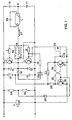
- FIG Operation of a low-pressure discharge lamp using a circuit diagram schematically shown The principle of the circuit arrangement according to the invention is shown in FIG Operation of a low-pressure discharge lamp using a circuit diagram schematically shown.
- This circuit is a self-oscillating half-bridge inverter, that of a parallel to the DC voltage input of the circuit Smoothing capacitor 1 is fed.
- the half-bridge inverter consists of essentially of two alternating switching transistors 2, 3, here as bipolar transistors shown, which form a half-bridge and each with a control for the base connection and with return diodes 4, 5 parallel to their switching path are provided.
- the bipolar transistors 2, 3 are controlled via a toroidal core transformer, whose secondary windings 6b, 6c each have a series resistor 7, 8 are guided to the base of a switching transistor 2, 3 and its primary winding 6a on the one hand with the center tap M of the half bridge and on the other hand via the lamp inductor 27 and the discharge path of the lamp L or via a parallel connected to the lamp L resonant capacitance 28 is connected to a tap A.
- the tap A is via a first coupling capacitor 10 to the collector of the Bipolar transistor 2 and via a second coupling capacitor 11 to the emitter of the bipolar transistor 3 out.
- the smoothing capacitor 1 charges to the full input voltage U.
- Switch transistors 2, 3 of the half bridge alternating with a switching frequency greater than 20 KHz. This means that the center tap is located M alternately on the positive or negative pole of the smoothing capacitor 1 while tap A with suitable dimensioning of the circuit components the potential U / 2 is thus flowing in the branch between the center tap M and the node A a medium frequency alternating current (greater than 20 KHz), the frequency of which is determined by the switching frequency of transistors 2, 3.
- Diac 14 is mainly responsible for starting the half-bridge inverter. Immediately after switching on the circuit arrangement builds on Capacitor 13 the breakover voltage of the diac 14, so that the diac 14 trigger pulses on the base of transistor 3 there. After starting the inverter the capacitor 13 discharged via the diode 16 so far that no further trigger pulses can be generated by the diac 14.
- the remaining elements 9 and 17 to 26 of the circuit arrangement which have not yet been explained belong to the shutdown device according to the invention, the inverter if the lamp L is defective or if there is an abnormal operating state switches off.
- the main component of this shutdown device is a bistable multivibrator, consisting of the bipolar transistors 17, 18 and the ohmic resistors 19 to 22, which drives the gate electrode of a field effect transistor 23.
- To for this purpose is an output of the bistable multivibrator, i.e. the collector of the Transistor 17, connected to the gate electrode of the field effect transistor 23.
- the Switching path, i.e. the drain-source path, of the field effect transistor 23 lies in parallel to the control electrode, i.e.
- An abnormal operating condition manifests itself in the circuit according to the preferred one Embodiment by an excessive compared to the normal operating state Voltage drop across the smoothing capacitor 1.
- the voltage across the smoothing capacitor 1 is made with the help of one consisting of ohmic resistors 24, 25 Voltage divider, which is connected in parallel to the smoothing capacitor 1, and by means of a Zener diode 26 sampled.
- the Zener diode 26 is parallel to the resistor 25 of the Arranged voltage divider and with the set or reset input of the bistable Multivibrators, i.e. connected to the base terminal of transistor 18.
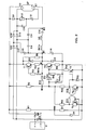
- FIG. 2 shows a detailed circuit diagram of a circuit arrangement according to the invention for operating a low-pressure discharge lamp, in particular for operating a Fluorescent lamp with an electrical power consumption between 9 and 13 watts.
- This circuit arrangement contains an essential component a self-oscillating half-bridge inverter from the DC voltage output a voltage source V is fed.
- the transistors T1, T2 of the half inverter are with a control device and series resistors R3 to R6 and arranged parallel to the switching paths of the transistors T1, T2 Return diodes D3, D4 provided.
- the transistors T1, T2 are activated via the secondary windings RK1b and RK1c of a toroidal transformer, which are each connected to the base of a transistor T1, T2.
- the primary winding RK1a of the toroidal transformer is integrated in the series resonant circuit, the from the center tap M between the transistors T1, T2 via the primary winding RK1a, the resonance inductance LD, the coupling capacitor C10, the resonance capacitance C9 and the lamp electrode E2 to the collector connection of the Transistor T1 extends.
- the resonance capacitance C9 is parallel to the discharge path the low-pressure discharge lamp LP switched.
- the circuit arrangement also contains an electrode heating circuit which preheats of the electrode filaments E1, E2 of the lamp LP and in addition to the electrode filaments E1, E2 also the PTC thermistor R12, the capacitances C12, C15 and the Diode D1 includes.
- the PTC thermistor bridges during the electrode preheating phase R12 is the capacitance C15 lying parallel to it.
- the electrode E2 of the lamp LP is connected to the positive pole of the smoothing capacitor C6, which is parallel to the switching paths of the transistors T1, T2 and parallel to the DC voltage output of the voltage source V is switched.
- This circuit arrangement also contains an active harmonic filter, which is a sinusoidal one Mains current drain enabled.
- the active harmonic filter consists of two Diode pairs D11, D13 and D12, D14 and from the capacitors C8 and C13.
- Both diode pairs are in the forward DC direction on the parallel to the DC output connected to the voltage source V supporting capacitor C5 and connected to the smoothing capacitor C6 via the electrode coil E2.
- Capacitor C13 is tapped between the diodes connected in series D12, D14 and with a node M1, which is potentially the center tap M corresponds, connected in the series resonance circuit, while the capacitor C8 with one tap between the diodes D11, D13 of the other connected in series Diode pair connected and led to node M1 in the series resonance circuit is.
- a diac DK and a start capacitor ensure that the half-bridge inverter starts to oscillate C7 and resistors R2, R8.
- the start capacitor C7 is on the one hand with the negative pole of the smoothing capacitor C6 and on the other hand over the Resistor R2 connected to the positive pole of the smoothing capacitor C6.
- the diac DK is connected in parallel to the starting capacitor C7 and to the base of the transistor T2 connected.
- a tap M3 between the start capacitor C7 and the Resistor R2 is via a resistor R15 and a diode D5 for center tap M of the inverter.
- the resistor R8 is parallel to the flyback diode D3 switched.
- a capacitor C14 arranged in parallel with the flyback diode D4 is reduced the power losses that occur when the inductors are magnetized, by slowing down the voltage edges generated by the inverter.
- the shutdown device comprises this circuit arrangement a bistable multivibrator made by transistors T3, T4 and ohmic Resistors R9, R10, R11, R13 is formed, and a field effect transistor T5, two Zener diodes D2, D6 and a voltage divider R1, R7 and an ohmic Resistor R14.
- the collector of transistor T4 is on the one hand via the resistor R10 with the tap M3 and on the other hand with the gate electrode of the field effect transistor T5 connected, and via the resistor R13 to the base of the transistor T3 led. Parallel to the collector-emitter path of transistor T4 and to the gate of the field effect transistor T5, the zener diode D2 is connected.
- the transistor T3 collector is connected to a node via the resistor R9 passed between the resistors R2 and R10 and with the resistor R11 connected to the base of transistor T4.
- the source of the field effect transistor T5 and the emitter connection of the transistors T3, T4 are with the negative pole of the smoothing capacitor C6.
- the one from the ohmic resistors R1, R7 existing voltage divider is parallel to the smoothing capacitor C6 and has a tap M4, which leads to the base of the transistor T3 via the Zener diode D6 is.
- the transistors T1, T2 of the half-bridge inverter switch alternately a frequency above 20 kHz, so that the center tap M alternately with the positive or negative pole of the smoothing capacitor C6 is connected during the Coupling capacitor C10 carries the voltage U / 2 when connected to the smoothing capacitor C6 applied voltage is denoted by U.
- U the voltage
- U the voltage
- the inverter swings through the diac DK, which gives trigger pulses to the base of transistor T2 after the starting capacitor C7 has previously charged to the breakdown voltage of the Diac DK.
- the low-pressure discharge lamp LP Before the low-pressure discharge lamp LP ignites, it first flows through the Electrode coils E1, E2, the capacitance C12 and the PTC thermistor R12 a heating current. After sufficient electrode preheating, the PTC thermistor R12 becomes high-resistance, so that to the now connected in series, arranged parallel to the lamp LP Capacities C12, C15 in interaction with the resonance inductance LD by means of Exaggerated resonance builds up the ignition voltage required for the lamp LP. The Lamp LP ignites and the lower operating voltage arises above the lamp a.
- the mode of operation of the diodes D11 to D14 and the capacitors C8, C13 existing active harmonic filter in combination with the resonance inductance LD and the capacitors C5, C6 is described in detail in DE 36 23 749 A1 and should therefore not be explained in more detail here.
- the active harmonic filter pumps energy from the. with the help of the capacitors C8, C9, C13 Series resonance circuit in the smoothing capacitor C6 back, so that an approximate sinusoidal mains current draw is possible.
- the bistable multivibrator consisting essentially of transistors T3, T4, is fed by the start capacitor C7. After switching on the circuit arrangement becomes the bistable multivibrator with that rising at the start capacitor C7 Voltage defined by resetting that through resistor R10 and the gate-source capacitance of the field effect transistor T5, the base-emitter voltage at the transistor T3 is delayed more than that at transistor T4, so that transistor T3 turns off while transistor T4 conducts.
- the field effect transistor T5 also blocks.
- the breakover voltage of the diac DK builds up at the start capacitor C7, so that this Trigger pulses on the base of transistor T2 there.
- An abnormal operating state of the half-bridge inverter manifests itself in the present circuit arrangement in an excessive voltage drop across the smoothing capacitor C6. Becomes a through the Zener diode D6, the voltage divider resistors R1, R7 and the transistor T3 defined threshold value exceeded, flows Base current for transistor T3 and the bistable multivibrator is reset, i.e. the switching path of transistor T3 conducts and blocks that of transistor T4. Of the Field effect transistor T5 is now switched through by the bistable multivibrator, see above that the base of the half-bridge transistor T2 through the resistor R14 and through the now conductive source-drain path of the field effect transistor T5 the control signal is withdrawn.
- the inverter is de-energized and the voltage at the starting capacitor C7 remains due to the load due to the resistance now connected in parallel R9 below the breakover voltage of the Diac DK. There are therefore no trigger pulses generated by the Diac DK.
- the inverter can only start again when the bistable multivibrator set again by interrupting the power supply becomes.
- the invention is not limited to the exemplary embodiment described in more detail above.
- the shutdown device according to the invention consisting of the electrical components 9 and 17 to 26, also in a circuit arrangement for Operation of low-voltage halogen bulbs can be integrated.
- the voltage divider 24, 25 is here, however, not connected in parallel to the input capacitor 1, but Part of the load or lamp circuit.
- the short circuit current in the Voltage divider resistors have an excessive voltage drop from the zener diode 26 is detected and leads to the triggering of the shutdown device.
- Voltage divider 24, 25 can be used in a circuit arrangement for low-voltage halogen incandescent lamps can also be replaced by a simple load or emitter resistor, with the emitter connection of the half-bridge transistor 3 and the negative pole of the Input capacitor 1 is connected, and to which the Zener diode 26 is connected in parallel is.
- the bistable multivibrator can save space as one in C-MOS technology implemented integrated circuit can be realized.
- Circuit arrangement is particularly suitable for a D flip-flop in which an indefinite one Initial state cannot occur. This opens up the possibility the circuit arrangement via a sensor, for example a touch contact with downstream evaluation logic, to be switched off externally by the clock input of the D flip-flop is controlled by the sensor.
- the shutdown device according to the invention can also be integrated into a full-bridge inverter.
- Dimensioning of the circuit according to FIG. 3 R1 2.2 M ⁇ , 1% R2 820 K ⁇ R3, R4 8.2 ⁇ R5, R6 0.56 ⁇ R7, R9 39 K ⁇ R8 510 K ⁇ R10, R11, R13 330 K ⁇ R14 0.22 ⁇ R15 33 K ⁇ C5 47 nF C6 10 ⁇ F C7 100 nF, 63 V C8 3.3 nF C9 5.6 nF C10 150 nF C12 10 nF C13 4.7 nF C14 1.0 nF C15 3.3 nF DK N413M T3, T4 BC547C T5 BSS295 D2 BZX55 / C10 D6 BZX55B7V5 LD 3 mH, EF16
Landscapes
- Circuit Arrangements For Discharge Lamps (AREA)
Claims (8)
- Montage pour faire fonctionner des lampes électriques, le montage ayant les caractéristiques suivantes:
Une alimentation à découpage qui est alimentée en tension continue et qui comporte au moins deux transistors (2,3;T1,T2) passant en alternance,caractérisé en ce que le dispositif d'arrêt a les caractéristiques suivantes:une commande des transistors (2,3;T1,T2) de l'alimentation à découpage,un condensateur (1;C6) de lissage monté parallèlement aux sections de commutation des transistors (2,3;T1,T2) de l'alimentation à découpageun dispositif d'arrêt, qui, en cas d'anomalie de fonctionnement du montage, arrête ce montage en prélevant d'au moins un transistor (3;T2) de l'alimentation à découpage le signal de commande destiné à son électrode de commande,un interrupteur (23;T5) électronique, qui peut être commandé, et dont la section de commutation est branchée en parallèle avec l'électrode de commande d'un transistor (3;T2) de l'alimentation à découpage,un multivibrateur (17,18;T3,T4) bistable, une sortie du multivibrateur (17,18;T3,T4) étant reliée à l'électrode de commande de l'interrupteur (23;T5) électronique et l'entrée d'impulsion de commande et de remise à l'état initial du multivibrateur (17,18;T3,T4) étant reliée à la sortie d'un interrupteur (26;D6) à valeur seuil. - Montage pour faire fonctionner des lampes électriques suivant la revendication 1, caractérisé en ce que l'interrupteur électronique pouvant être commandé est un transistor (23;T5) à effet de champ.
- Montage pour faire fonctionner des lampes électriques suivant la revendication 1, caractérisé en ce que l'alimentation à découpage est un onduleur à demi-pont auto-hétérodyne.
- Montage pour faire fonctionner des lampes électriques suivant la revendication 1, caractérisé en ce que l'interrupteur (26;D6) à valeur seuil est branché en parallèle avec une résistance (25;R7) d'un diviseur (24,25;R1,R7) de tension, le diviseur (24,25;R1,R7) de tension étant monté en parallèle au condensateur (1;C6) de lissage.
- Montage pour faire fonctionner des lampes électriques suivant la revendication 1, caractérisé en ce que le multivibrateur bistable est un circuit intégré réalisé en technique C-MOS.
- Montage pour faire fonctionner des lampes électriques suivant la revendication 5, caractérisé en ce que le multivibrateur bistable est une bascule D.
- Montage pour faire fonctionner des lampes électriques suivant la revendication 6, caractérisé en ce que l'entrée de cadence de la bascule D est commandée par un capteur comportant une logique d'exploitation en aval.
- Montage pour faire fonctionner des lampes électriques suivant la revendication 7, caractérisé en ce que le capteur est un contact direct.
Applications Claiming Priority (2)
| Application Number | Priority Date | Filing Date | Title |
|---|---|---|---|
| DE4334076A DE4334076A1 (de) | 1993-10-06 | 1993-10-06 | Schaltungsanordnung zum Betrieb elektrischer Lampen |
| DE4334076 | 1993-10-06 |
Publications (2)
| Publication Number | Publication Date |
|---|---|
| EP0648068A1 EP0648068A1 (fr) | 1995-04-12 |
| EP0648068B1 true EP0648068B1 (fr) | 1998-08-12 |
Family
ID=6499549
Family Applications (1)
| Application Number | Title | Priority Date | Filing Date |
|---|---|---|---|
| EP94113515A Revoked EP0648068B1 (fr) | 1993-10-06 | 1994-08-30 | Circuit d'alimentation de lampes électriques |
Country Status (2)
| Country | Link |
|---|---|
| EP (1) | EP0648068B1 (fr) |
| DE (2) | DE4334076A1 (fr) |
Families Citing this family (6)
| Publication number | Priority date | Publication date | Assignee | Title |
|---|---|---|---|---|
| DE19505459A1 (de) * | 1995-02-17 | 1996-08-22 | Patent Treuhand Ges Fuer Elektrische Gluehlampen Mbh | Schaltungsanordnung zum Betrieb einer Entladungslampe |
| JP3210561B2 (ja) * | 1995-06-14 | 2001-09-17 | 株式会社小糸製作所 | 放電灯点灯回路 |
| US5783911A (en) * | 1995-07-12 | 1998-07-21 | Patent-Treuhand-Gesellschaft Fuer Elektrische Gluehlampen Mbh | Circuit arrangement for operating electric lamps, and operating method for electric lamps |
| US6005354A (en) * | 1996-10-21 | 1999-12-21 | International Rectifier Corporation | Ballast IC with shut-down function |
| EP1438879A1 (fr) * | 2001-10-01 | 2004-07-21 | Koninklijke Philips Electronics N.V. | Circuit en pont auto-oscillant comprenant un circuit de demarrage |
| DE102005028419A1 (de) * | 2005-06-20 | 2006-12-28 | Patent-Treuhand-Gesellschaft für elektrische Glühlampen mbH | Abschaltschaltung |
Family Cites Families (3)
| Publication number | Priority date | Publication date | Assignee | Title |
|---|---|---|---|---|
| US4538095A (en) * | 1983-06-03 | 1985-08-27 | Nilssen Ole K | Series-resonant electronic ballast circuit |
| US4680506A (en) * | 1984-12-10 | 1987-07-14 | Nilssen Ole K | Inverter-type microwave oven power supply |
| DE3700421A1 (de) * | 1987-01-08 | 1988-07-21 | Patent Treuhand Ges Fuer Elektrische Gluehlampen Mbh | Schaltungsanordnung zum betrieb einer niederdruckentladungslampe |
-
1993
- 1993-10-06 DE DE4334076A patent/DE4334076A1/de not_active Withdrawn
-
1994
- 1994-08-30 EP EP94113515A patent/EP0648068B1/fr not_active Revoked
- 1994-08-30 DE DE59406663T patent/DE59406663D1/de not_active Revoked
Also Published As
| Publication number | Publication date |
|---|---|
| DE4334076A1 (de) | 1995-06-08 |
| DE59406663D1 (de) | 1998-09-17 |
| EP0648068A1 (fr) | 1995-04-12 |
Similar Documents
| Publication | Publication Date | Title |
|---|---|---|
| DE2941822C2 (fr) | ||
| EP0679046B1 (fr) | Circuit pour alimenter des lampes à décharge basse-pression | |
| EP0798952B1 (fr) | Circuit pour l'opération de lampes électriques et procédé d'opération | |
| EP0239793B1 (fr) | Disposition de circuit pour la mise en oeuvre de lampes à décharge basse pression | |
| EP0264765B1 (fr) | Disposition de circuit pour la mise en oeuvre de lampe à incandescence halogène basse tension | |
| EP0800335B1 (fr) | Circuit pour alimenter des lampes électriques | |
| EP0062275B1 (fr) | Ballast pour le fonctionnement de lampes à décharge à basse pression | |
| WO1993012631A1 (fr) | Circuit pour actionner une ou plusieurs lampe(s) a decharge a basse pression | |
| EP0693864B1 (fr) | Circuit pour alimenter une ou plusieurs lampes à décharge basse-pression | |
| EP0062276B1 (fr) | Ballast pour le fonctionnement de lampes à décharge à basse pression | |
| DE69315761T2 (de) | Geschützter Umrichter zur Steuerung einer Entladungslampe | |
| DE19819027A1 (de) | Schaltungsanordnung zum Betrieb mindestens einer Entladungslampe | |
| EP0753987B1 (fr) | Circuit et procédé d'opération de lampes électriques | |
| EP0648068B1 (fr) | Circuit d'alimentation de lampes électriques | |
| EP1608208B1 (fr) | Circuit avec dispositif de coupure pour alimenter des sources lumineuses | |
| DE19715341C1 (de) | Elektronisches Vorschaltgerät mit automatischem Wiederanlauf | |
| DE3137940C2 (de) | Elektronisches Vorschaltgerät für mindestens eine Leuchtstofflampe | |
| DE3504803A1 (de) | Gegentaktgenerator | |
| EP0276460A1 (fr) | Disposition de circuit pour mettre en oeuvre une lampe à décharge basse pression | |
| DE1803486A1 (de) | Schaltungsanordnung zum Betrieb eines selbstgesteuerten Transistorwechselrichters | |
| DE4143488C2 (de) | Elektronisches Vorschaltgerät | |
| DE3013805A1 (de) | Schaltung zum starten und stabilisieren einer bogenentladungslampe | |
| DE3429773C2 (fr) | ||
| DE2954614C2 (fr) | ||
| EP0541908A1 (fr) | Circuit pour alimenter une ou plusieurs lampes à décharge à basse pression |
Legal Events
| Date | Code | Title | Description |
|---|---|---|---|
| PUAI | Public reference made under article 153(3) epc to a published international application that has entered the european phase |
Free format text: ORIGINAL CODE: 0009012 |
|
| AK | Designated contracting states |
Kind code of ref document: A1 Designated state(s): BE DE FR GB IT NL |
|
| 17P | Request for examination filed |
Effective date: 19950518 |
|
| GRAG | Despatch of communication of intention to grant |
Free format text: ORIGINAL CODE: EPIDOS AGRA |
|
| 17Q | First examination report despatched |
Effective date: 19971202 |
|
| GRAG | Despatch of communication of intention to grant |
Free format text: ORIGINAL CODE: EPIDOS AGRA |
|
| GRAH | Despatch of communication of intention to grant a patent |
Free format text: ORIGINAL CODE: EPIDOS IGRA |
|
| GRAH | Despatch of communication of intention to grant a patent |
Free format text: ORIGINAL CODE: EPIDOS IGRA |
|
| GRAA | (expected) grant |
Free format text: ORIGINAL CODE: 0009210 |
|
| AK | Designated contracting states |
Kind code of ref document: B1 Designated state(s): BE DE FR GB IT NL |
|
| REF | Corresponds to: |
Ref document number: 59406663 Country of ref document: DE Date of ref document: 19980917 |
|
| GBT | Gb: translation of ep patent filed (gb section 77(6)(a)/1977) |
Effective date: 19981013 |
|
| ET | Fr: translation filed | ||
| PLBQ | Unpublished change to opponent data |
Free format text: ORIGINAL CODE: EPIDOS OPPO |
|
| PLBI | Opposition filed |
Free format text: ORIGINAL CODE: 0009260 |
|
| PLBF | Reply of patent proprietor to notice(s) of opposition |
Free format text: ORIGINAL CODE: EPIDOS OBSO |
|
| 26 | Opposition filed |
Opponent name: VOSSLOH-SCHWABE GMBH Effective date: 19990512 |
|
| PLBF | Reply of patent proprietor to notice(s) of opposition |
Free format text: ORIGINAL CODE: EPIDOS OBSO |
|
| PGFP | Annual fee paid to national office [announced via postgrant information from national office to epo] |
Ref country code: DE Payment date: 20011022 Year of fee payment: 8 |
|
| REG | Reference to a national code |
Ref country code: GB Ref legal event code: IF02 |
|
| RDAH | Patent revoked |
Free format text: ORIGINAL CODE: EPIDOS REVO |
|
| PGFP | Annual fee paid to national office [announced via postgrant information from national office to epo] |
Ref country code: GB Payment date: 20020808 Year of fee payment: 9 |
|
| PGFP | Annual fee paid to national office [announced via postgrant information from national office to epo] |
Ref country code: NL Payment date: 20020813 Year of fee payment: 9 |
|
| PGFP | Annual fee paid to national office [announced via postgrant information from national office to epo] |
Ref country code: BE Payment date: 20020820 Year of fee payment: 9 |
|
| PGFP | Annual fee paid to national office [announced via postgrant information from national office to epo] |
Ref country code: FR Payment date: 20020829 Year of fee payment: 9 |
|
| RDAG | Patent revoked |
Free format text: ORIGINAL CODE: 0009271 |
|
| STAA | Information on the status of an ep patent application or granted ep patent |
Free format text: STATUS: PATENT REVOKED |
|
| 27W | Patent revoked |
Effective date: 20020630 |
|
| GBPR | Gb: patent revoked under art. 102 of the ep convention designating the uk as contracting state |
Free format text: 20020630 |
|
| NLR2 | Nl: decision of opposition |
Effective date: 20020630 |