EP0648068B1 - Circuit for operating electrical lamps - Google Patents
Circuit for operating electrical lamps Download PDFInfo
- Publication number
- EP0648068B1 EP0648068B1 EP94113515A EP94113515A EP0648068B1 EP 0648068 B1 EP0648068 B1 EP 0648068B1 EP 94113515 A EP94113515 A EP 94113515A EP 94113515 A EP94113515 A EP 94113515A EP 0648068 B1 EP0648068 B1 EP 0648068B1
- Authority
- EP
- European Patent Office
- Prior art keywords
- circuit arrangement
- transistor
- circuit
- switched
- electric lamps
- Prior art date
- Legal status (The legal status is an assumption and is not a legal conclusion. Google has not performed a legal analysis and makes no representation as to the accuracy of the status listed.)
- Revoked
Links
Images
Classifications
-
- H—ELECTRICITY
- H05—ELECTRIC TECHNIQUES NOT OTHERWISE PROVIDED FOR
- H05B—ELECTRIC HEATING; ELECTRIC LIGHT SOURCES NOT OTHERWISE PROVIDED FOR; CIRCUIT ARRANGEMENTS FOR ELECTRIC LIGHT SOURCES, IN GENERAL
- H05B41/00—Circuit arrangements or apparatus for igniting or operating discharge lamps
- H05B41/14—Circuit arrangements
- H05B41/26—Circuit arrangements in which the lamp is fed by power derived from dc by means of a converter, e.g. by high-voltage dc
- H05B41/28—Circuit arrangements in which the lamp is fed by power derived from dc by means of a converter, e.g. by high-voltage dc using static converters
- H05B41/282—Circuit arrangements in which the lamp is fed by power derived from dc by means of a converter, e.g. by high-voltage dc using static converters with semiconductor devices
- H05B41/285—Arrangements for protecting lamps or circuits against abnormal operating conditions
- H05B41/2851—Arrangements for protecting lamps or circuits against abnormal operating conditions for protecting the circuit against abnormal operating conditions
- H05B41/2855—Arrangements for protecting lamps or circuits against abnormal operating conditions for protecting the circuit against abnormal operating conditions against abnormal lamp operating conditions
Definitions
- the invention relates to a circuit arrangement for operating electric lamps according to the preamble of claim 1.
- Such a circuit arrangement is disclosed, for example, in EP 0 276 460 B1. It is used to operate a low-pressure discharge lamp and has an inverter on that of two alternately switching, arranged in a half-bridge Transistors.
- This circuit arrangement has a safety shutdown, which shuts down the inverter during abnormal operation.
- the shutdown device consists essentially of a thyristor, which is parallel to the control electrode Switching transistor of the inverter is switched, and from a Zener diode that the Gate of the thyristor controls. In the event of an abnormal operating state, the thyristor switches through and withdraws the control signal from a switching transistor of the inverter and thus causes the circuit arrangement to be shut down.
- the circuit arrangement according to the invention has a shutdown device, which at the operating device is switched off in the event of an abnormal operating state.
- This shutdown device consists essentially of a controllable electronic switch, in particular a field effect transistor, the switching path parallel to the control path a transistor of the switching power supply is switched, and a bistable multivibrator, from which an output with the control electrode of the electronic switch is connected, as well as from a threshold switch, which is connected to an input of the bistable Multivibrators is connected. If there is an abnormal operating state, e.g. in the case of a defective lamp, the threshold switch switches through and sets the bistable multivibrator, making the switching path of the controllable electronic Switch is conductive and thus a transistor of the switching power supply Control signal is withdrawn.
- the circuit arrangement according to the invention takes up less space than that in Circuit disclosed above as prior art patent EP 0 274 460 B1 the circuit according to the invention on large-volume ohmic resistors with some Watts resilience waived. It is even possible to switch off the device according to the invention Circuit arrangement extremely compact in SMD technology. In addition, this switch-off device can in principle in any inverter to get integrated.
- the use of a bistable multivibrator in the shutdown device the circuit arrangement according to the invention offers the further advantage that this circuit on an external switching on / off of the lamp operating device is prepared. Via additional sensors, for example a touch contact with a subsequent evaluation logic, the bistable multivibrator can too externally controlled and thus the control gear can be switched on and off. In order to the possibility is created in a lighting system that has a larger Number of lamps and operating devices, individual lamps or lamp groups to switch separately.
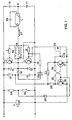
- FIG Operation of a low-pressure discharge lamp using a circuit diagram schematically shown The principle of the circuit arrangement according to the invention is shown in FIG Operation of a low-pressure discharge lamp using a circuit diagram schematically shown.
- This circuit is a self-oscillating half-bridge inverter, that of a parallel to the DC voltage input of the circuit Smoothing capacitor 1 is fed.
- the half-bridge inverter consists of essentially of two alternating switching transistors 2, 3, here as bipolar transistors shown, which form a half-bridge and each with a control for the base connection and with return diodes 4, 5 parallel to their switching path are provided.
- the bipolar transistors 2, 3 are controlled via a toroidal core transformer, whose secondary windings 6b, 6c each have a series resistor 7, 8 are guided to the base of a switching transistor 2, 3 and its primary winding 6a on the one hand with the center tap M of the half bridge and on the other hand via the lamp inductor 27 and the discharge path of the lamp L or via a parallel connected to the lamp L resonant capacitance 28 is connected to a tap A.
- the tap A is via a first coupling capacitor 10 to the collector of the Bipolar transistor 2 and via a second coupling capacitor 11 to the emitter of the bipolar transistor 3 out.
- the smoothing capacitor 1 charges to the full input voltage U.
- Switch transistors 2, 3 of the half bridge alternating with a switching frequency greater than 20 KHz. This means that the center tap is located M alternately on the positive or negative pole of the smoothing capacitor 1 while tap A with suitable dimensioning of the circuit components the potential U / 2 is thus flowing in the branch between the center tap M and the node A a medium frequency alternating current (greater than 20 KHz), the frequency of which is determined by the switching frequency of transistors 2, 3.
- Diac 14 is mainly responsible for starting the half-bridge inverter. Immediately after switching on the circuit arrangement builds on Capacitor 13 the breakover voltage of the diac 14, so that the diac 14 trigger pulses on the base of transistor 3 there. After starting the inverter the capacitor 13 discharged via the diode 16 so far that no further trigger pulses can be generated by the diac 14.
- the remaining elements 9 and 17 to 26 of the circuit arrangement which have not yet been explained belong to the shutdown device according to the invention, the inverter if the lamp L is defective or if there is an abnormal operating state switches off.
- the main component of this shutdown device is a bistable multivibrator, consisting of the bipolar transistors 17, 18 and the ohmic resistors 19 to 22, which drives the gate electrode of a field effect transistor 23.
- To for this purpose is an output of the bistable multivibrator, i.e. the collector of the Transistor 17, connected to the gate electrode of the field effect transistor 23.
- the Switching path, i.e. the drain-source path, of the field effect transistor 23 lies in parallel to the control electrode, i.e.
- An abnormal operating condition manifests itself in the circuit according to the preferred one Embodiment by an excessive compared to the normal operating state Voltage drop across the smoothing capacitor 1.
- the voltage across the smoothing capacitor 1 is made with the help of one consisting of ohmic resistors 24, 25 Voltage divider, which is connected in parallel to the smoothing capacitor 1, and by means of a Zener diode 26 sampled.
- the Zener diode 26 is parallel to the resistor 25 of the Arranged voltage divider and with the set or reset input of the bistable Multivibrators, i.e. connected to the base terminal of transistor 18.
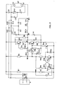
- FIG. 2 shows a detailed circuit diagram of a circuit arrangement according to the invention for operating a low-pressure discharge lamp, in particular for operating a Fluorescent lamp with an electrical power consumption between 9 and 13 watts.
- This circuit arrangement contains an essential component a self-oscillating half-bridge inverter from the DC voltage output a voltage source V is fed.
- the transistors T1, T2 of the half inverter are with a control device and series resistors R3 to R6 and arranged parallel to the switching paths of the transistors T1, T2 Return diodes D3, D4 provided.
- the transistors T1, T2 are activated via the secondary windings RK1b and RK1c of a toroidal transformer, which are each connected to the base of a transistor T1, T2.
- the primary winding RK1a of the toroidal transformer is integrated in the series resonant circuit, the from the center tap M between the transistors T1, T2 via the primary winding RK1a, the resonance inductance LD, the coupling capacitor C10, the resonance capacitance C9 and the lamp electrode E2 to the collector connection of the Transistor T1 extends.
- the resonance capacitance C9 is parallel to the discharge path the low-pressure discharge lamp LP switched.
- the circuit arrangement also contains an electrode heating circuit which preheats of the electrode filaments E1, E2 of the lamp LP and in addition to the electrode filaments E1, E2 also the PTC thermistor R12, the capacitances C12, C15 and the Diode D1 includes.
- the PTC thermistor bridges during the electrode preheating phase R12 is the capacitance C15 lying parallel to it.
- the electrode E2 of the lamp LP is connected to the positive pole of the smoothing capacitor C6, which is parallel to the switching paths of the transistors T1, T2 and parallel to the DC voltage output of the voltage source V is switched.
- This circuit arrangement also contains an active harmonic filter, which is a sinusoidal one Mains current drain enabled.
- the active harmonic filter consists of two Diode pairs D11, D13 and D12, D14 and from the capacitors C8 and C13.
- Both diode pairs are in the forward DC direction on the parallel to the DC output connected to the voltage source V supporting capacitor C5 and connected to the smoothing capacitor C6 via the electrode coil E2.
- Capacitor C13 is tapped between the diodes connected in series D12, D14 and with a node M1, which is potentially the center tap M corresponds, connected in the series resonance circuit, while the capacitor C8 with one tap between the diodes D11, D13 of the other connected in series Diode pair connected and led to node M1 in the series resonance circuit is.
- a diac DK and a start capacitor ensure that the half-bridge inverter starts to oscillate C7 and resistors R2, R8.
- the start capacitor C7 is on the one hand with the negative pole of the smoothing capacitor C6 and on the other hand over the Resistor R2 connected to the positive pole of the smoothing capacitor C6.
- the diac DK is connected in parallel to the starting capacitor C7 and to the base of the transistor T2 connected.
- a tap M3 between the start capacitor C7 and the Resistor R2 is via a resistor R15 and a diode D5 for center tap M of the inverter.
- the resistor R8 is parallel to the flyback diode D3 switched.
- a capacitor C14 arranged in parallel with the flyback diode D4 is reduced the power losses that occur when the inductors are magnetized, by slowing down the voltage edges generated by the inverter.
- the shutdown device comprises this circuit arrangement a bistable multivibrator made by transistors T3, T4 and ohmic Resistors R9, R10, R11, R13 is formed, and a field effect transistor T5, two Zener diodes D2, D6 and a voltage divider R1, R7 and an ohmic Resistor R14.
- the collector of transistor T4 is on the one hand via the resistor R10 with the tap M3 and on the other hand with the gate electrode of the field effect transistor T5 connected, and via the resistor R13 to the base of the transistor T3 led. Parallel to the collector-emitter path of transistor T4 and to the gate of the field effect transistor T5, the zener diode D2 is connected.
- the transistor T3 collector is connected to a node via the resistor R9 passed between the resistors R2 and R10 and with the resistor R11 connected to the base of transistor T4.
- the source of the field effect transistor T5 and the emitter connection of the transistors T3, T4 are with the negative pole of the smoothing capacitor C6.
- the one from the ohmic resistors R1, R7 existing voltage divider is parallel to the smoothing capacitor C6 and has a tap M4, which leads to the base of the transistor T3 via the Zener diode D6 is.
- the transistors T1, T2 of the half-bridge inverter switch alternately a frequency above 20 kHz, so that the center tap M alternately with the positive or negative pole of the smoothing capacitor C6 is connected during the Coupling capacitor C10 carries the voltage U / 2 when connected to the smoothing capacitor C6 applied voltage is denoted by U.
- U the voltage
- U the voltage
- the inverter swings through the diac DK, which gives trigger pulses to the base of transistor T2 after the starting capacitor C7 has previously charged to the breakdown voltage of the Diac DK.
- the low-pressure discharge lamp LP Before the low-pressure discharge lamp LP ignites, it first flows through the Electrode coils E1, E2, the capacitance C12 and the PTC thermistor R12 a heating current. After sufficient electrode preheating, the PTC thermistor R12 becomes high-resistance, so that to the now connected in series, arranged parallel to the lamp LP Capacities C12, C15 in interaction with the resonance inductance LD by means of Exaggerated resonance builds up the ignition voltage required for the lamp LP. The Lamp LP ignites and the lower operating voltage arises above the lamp a.
- the mode of operation of the diodes D11 to D14 and the capacitors C8, C13 existing active harmonic filter in combination with the resonance inductance LD and the capacitors C5, C6 is described in detail in DE 36 23 749 A1 and should therefore not be explained in more detail here.
- the active harmonic filter pumps energy from the. with the help of the capacitors C8, C9, C13 Series resonance circuit in the smoothing capacitor C6 back, so that an approximate sinusoidal mains current draw is possible.
- the bistable multivibrator consisting essentially of transistors T3, T4, is fed by the start capacitor C7. After switching on the circuit arrangement becomes the bistable multivibrator with that rising at the start capacitor C7 Voltage defined by resetting that through resistor R10 and the gate-source capacitance of the field effect transistor T5, the base-emitter voltage at the transistor T3 is delayed more than that at transistor T4, so that transistor T3 turns off while transistor T4 conducts.
- the field effect transistor T5 also blocks.
- the breakover voltage of the diac DK builds up at the start capacitor C7, so that this Trigger pulses on the base of transistor T2 there.
- An abnormal operating state of the half-bridge inverter manifests itself in the present circuit arrangement in an excessive voltage drop across the smoothing capacitor C6. Becomes a through the Zener diode D6, the voltage divider resistors R1, R7 and the transistor T3 defined threshold value exceeded, flows Base current for transistor T3 and the bistable multivibrator is reset, i.e. the switching path of transistor T3 conducts and blocks that of transistor T4. Of the Field effect transistor T5 is now switched through by the bistable multivibrator, see above that the base of the half-bridge transistor T2 through the resistor R14 and through the now conductive source-drain path of the field effect transistor T5 the control signal is withdrawn.
- the inverter is de-energized and the voltage at the starting capacitor C7 remains due to the load due to the resistance now connected in parallel R9 below the breakover voltage of the Diac DK. There are therefore no trigger pulses generated by the Diac DK.
- the inverter can only start again when the bistable multivibrator set again by interrupting the power supply becomes.
- the invention is not limited to the exemplary embodiment described in more detail above.
- the shutdown device according to the invention consisting of the electrical components 9 and 17 to 26, also in a circuit arrangement for Operation of low-voltage halogen bulbs can be integrated.
- the voltage divider 24, 25 is here, however, not connected in parallel to the input capacitor 1, but Part of the load or lamp circuit.
- the short circuit current in the Voltage divider resistors have an excessive voltage drop from the zener diode 26 is detected and leads to the triggering of the shutdown device.
- Voltage divider 24, 25 can be used in a circuit arrangement for low-voltage halogen incandescent lamps can also be replaced by a simple load or emitter resistor, with the emitter connection of the half-bridge transistor 3 and the negative pole of the Input capacitor 1 is connected, and to which the Zener diode 26 is connected in parallel is.
- the bistable multivibrator can save space as one in C-MOS technology implemented integrated circuit can be realized.
- Circuit arrangement is particularly suitable for a D flip-flop in which an indefinite one Initial state cannot occur. This opens up the possibility the circuit arrangement via a sensor, for example a touch contact with downstream evaluation logic, to be switched off externally by the clock input of the D flip-flop is controlled by the sensor.
- the shutdown device according to the invention can also be integrated into a full-bridge inverter.
- Dimensioning of the circuit according to FIG. 3 R1 2.2 M ⁇ , 1% R2 820 K ⁇ R3, R4 8.2 ⁇ R5, R6 0.56 ⁇ R7, R9 39 K ⁇ R8 510 K ⁇ R10, R11, R13 330 K ⁇ R14 0.22 ⁇ R15 33 K ⁇ C5 47 nF C6 10 ⁇ F C7 100 nF, 63 V C8 3.3 nF C9 5.6 nF C10 150 nF C12 10 nF C13 4.7 nF C14 1.0 nF C15 3.3 nF DK N413M T3, T4 BC547C T5 BSS295 D2 BZX55 / C10 D6 BZX55B7V5 LD 3 mH, EF16
Description
Die Erfindung betrifft eine Schaltungsanordnung zum Betrieb elektrischer Lampen
gemäß dem Oberbegriff des Patentanspruchs 1.The invention relates to a circuit arrangement for operating electric lamps
according to the preamble of
Eine derartige Schaltungsanordnung ist beispielsweise in der EP 0 276 460 B1 offenbart.
Sie dient zum Betrieb einer Niederdruckentladungslampe und weist einen Wechselrichter
auf, der aus zwei alternierend schaltenden, in einer Halbbrücke angeordneten
Transistoren besteht. Diese Schaltungsanordnung besitzt eine Sicherheitsabschaltung,
die den Wechselrichter bei anomalen Betrieb stillegt. Die Abschaltvorrichtung
besteht im wesentlichen aus einem Thyristor, der parallel zur Steuerelektrode eines
Schalttransistors des Wechselrichters geschaltet ist, und aus einer Zenerdiode, die das
Gate des Thyristors steuert. Bei einem anomalen Betriebszustand schaltet der Thyristor
durch und entzieht einem Schalttransistor des Wechselrichters das Steuersignal
und bewirkt so eine Stillegung der Schaltungsanordnung. Zur Realisierung dieser
Sicherheitsabschaltung werden ein spannungsfester Thyristor sowie mehrere relativ
großvolumige ohmsche Widerstände mit einigen Watt Belastbarkeit benötigt, die zur
Strombegrenzung im Abschaltfall und zur Erzeugung des Thyristor-Haltestromes
dienen.Such a circuit arrangement is disclosed, for example, in
Es ist die Aufgabe der Erfindung, eine Schaltungsanordnung zum Betrieb elektrischer Lampen bereitzustellen, die eine möglichst einfache, universell anwendbare und kostengünstige Sicherheitsabschaltung besitzt, die die Schaltungsanordnung bei einem anomalen Betriebszustand zuverlässig abschaltet.It is the object of the invention to provide a circuit arrangement for operating electrical Provide lamps that are as simple, universally applicable and cost-effective as possible Has safety shutdown, which the circuit arrangement at a reliably switches off the abnormal operating state.
Diese Aufgabe wird erfindungsgemäß durch die kennzeichnenden Merkmale des Patentanspruchs
1 gelöst. Besonders vorteilhafte Ausführungen der Erfindung sind in
den Unteransprüchen beschrieben.This object is achieved by the characterizing features of the
Die erfindungsgemäße Schaltungsanordnung besitzt eine Abschaltvorrichtung, die bei einem anomalen Betriebszustand das Betriebs gerät abgeschaltet. Diese Abschaltvorrichtung besteht im wesentlichen aus einem steuerbaren elektronischen Schalter, insbesondere einem Feldeffekttransistor, dessen Schaltstrecke parallel zur Steuerstrecke eines Transistors des Schaltnetzteils geschaltet ist, und aus einem bistabilen Multivibrator, von dem ein Ausgang mit der Steuerelektrode des elektronischen Schalters verbunden ist, sowie aus einem Schwellwertschalter, der mit einem Eingang des bistabilen Multivibrators verschaltet ist. Bei Vorliegen eines anomalen Betriebszustandes, z.B im Fall einer defekten Lampe, schaltet der Schwellwertschalter durch und setzt den bistabilen Multivibrator, wodurch die Schaltstrecke des steuerbaren elektronischen Schalters leitfähig wird und damit einem Transistor des Schaltnetzteiles das Steuersignal entzogen wird.The circuit arrangement according to the invention has a shutdown device, which at the operating device is switched off in the event of an abnormal operating state. This shutdown device consists essentially of a controllable electronic switch, in particular a field effect transistor, the switching path parallel to the control path a transistor of the switching power supply is switched, and a bistable multivibrator, from which an output with the control electrode of the electronic switch is connected, as well as from a threshold switch, which is connected to an input of the bistable Multivibrators is connected. If there is an abnormal operating state, e.g. in the case of a defective lamp, the threshold switch switches through and sets the bistable multivibrator, making the switching path of the controllable electronic Switch is conductive and thus a transistor of the switching power supply Control signal is withdrawn.
Die erfindungsgemäße Schaltungsanordnung beansprucht weniger Raum als die im
oben als Stand der Technik zitierten Patent EP 0 274 460 B1 offenbarte Schaltung, da
die erfindungsgemäße Schaltung auf großvolumige ohmsche Widerstände mit einigen
Watt Belastbarkeit verzichtet. Es ist sogar möglich, die Abschaltvorrichtung der erfindungsgemäßen
Schaltungsanordnung äußerst kompakt in SMD-Technologie auszuführen.
Außerdem kann diese Abschaltvorrichtung prinzipiell in jeden Wechselrichter
integriert werden. Die Verwendung eines bistabilen Multivibrators in der Abschaltvorrichtung
der erfindungsgemäßen Schaltungsanordnung bietet den weiteren Vorteil,
daß diese Schaltung auf ein externes Ein-/Ausschalten des Lampenbetriebsgerätes
vorbereitet ist. Über eine zusätzliche Sensorik, beispielsweise einen Berührungskontakt
mit nachgeschalteter Auswertungslogik, kann der bistabile Multivibrator auch
extern gesteuert und somit das Betriebsgerät ein- und ausgeschaltet werden. Damit
wird die Möglichkeit geschaffen, in einer Beleuchtungsanlage, die eine größere
Anzahl von Lampen und Betriebsgeräten umfaßt, einzelne Lampen oder Lampengruppen
separat zu schalten.The circuit arrangement according to the invention takes up less space than that in
Circuit disclosed above as prior
Die Erfindung wird nachstehend anhand eines bevorzugten Ausführungsbeispiels näher erläutert. Es zeigen:
Figur 1- Eine schematisierte Schaltskizze einer erfindungsgemäßen Schaltungsanordnung zum Betrieb einer Niederdruckentladungslampe
Figur 2- Ein detailliertes Schaltbild der erfindungsgemäßen Schaltungsanordnung zum Betrieb einer Niederdruckentladungslampe
- Figure 1
- A schematic circuit diagram of a circuit arrangement according to the invention for operating a low-pressure discharge lamp
- Figure 2
- A detailed circuit diagram of the circuit arrangement according to the invention for operating a low-pressure discharge lamp
In der Figur 1 ist das Prinzip der erfindungsgemäßen Schaltungsanordnung zum Betrieb einer Niederdruckentladungslampe anhand einer Schaltskizze schematisch dargestellt. The principle of the circuit arrangement according to the invention is shown in FIG Operation of a low-pressure discharge lamp using a circuit diagram schematically shown.
Bei dieser Schaltung handelt es sich um einen selbstschwingenden Halbbrückenwechselrichter,
der von einem parallel zum Gleichspannungseingang der Schaltung liegenden
Glättungskondensator 1 gespeist wird. Der Halbbrückenwechselrichter besteht im
wesentlichen aus zwei alternierend schaltenden Transistoren 2, 3, hier als Bipolar-Transistoren
dargestellt, die eine Halbbrücke bilden und jeweils mit einer Ansteuerung
für den Basisanschluß sowie mit Rücklaufdioden 4, 5 parallel zu ihrer Schaltstrecke
versehen sind. Die Ansteuerung der Bipolar-Transistoren 2, 3 erfolgt über einen Ringkern-Transformator,
dessen Sekundärwicklungen 6b, 6c jeweils über einen Vorwiderstand
7, 8 zur Basis eines Schalttransistors 2, 3 geführt sind und dessen Primärwicklung
6a einerseits mit dem Mittenabgriff M der Halbbrücke sowie andererseits über
die Lampendrossel 27 und die Entladungsstrecke der Lampe L bzw. über eine parallel
zur Lampe L geschaltete Resonanzkapazität 28 mit einem Abgriff A verbunden ist.
Der Abgriff A ist über einen ersten Kopplungskondensator 10 zum Kollektor des
Bipolar-Transistors 2 und über einen zweiten Kopplungskondensator 11 zum Emitter
des Bipolar-Transistors 3 geführt. Die Induktivität 27 und die Kapazität 28 bilden
einen Serienresonanzkreis, der es ermöglicht, nach ausreichender Vorheizung der
Lampenelektroden an der Kapazität 28 durch Resonanzüberhöhung die Zündspannung
für die Niederdruckentladungslampe L bereitzustellen.This circuit is a self-oscillating half-bridge inverter,
that of a parallel to the DC voltage input of the
Zum Anlauf des Halbbrückenwechselrichters dienen ein Widerstand 12, ein Kondensator
13 und ein parallel zum Kondensator 13 angeordneter Diac 14, der über einen
ohmschen Widerstand 15 zur Basis des Transistors 3 geführt ist. Eine zusätzliche Diode
16, die mit dem Knotenpunkt B zwischen Widerstand 12, Kondensator 13, und
Diac 14 und mit dem Mittenabgriff M verbunden ist, sorgt für eine Stillegung dieser
Startschaltung bei arbeitendem Wechselrichter.A
Soweit entspricht diese Schaltungsanordnung einer typischen selbstschwingenden Halbbrückenschaltung, wie sie beispielsweise im Buch "Schaltnetzteile" von W. Hirschmann/A. Hauenstein, Hrsg. Siemens AG, Ausgabe 1990 auf Seite 63 beschrieben ist.As far as this circuit arrangement corresponds to a typical self-oscillating Half-bridge circuit, as described, for example, in W.'s book "Schaltnetzteile" Hirschmann / A. Hauenstein, ed. Siemens AG, 1990 edition on page 63 is.
Nach dem Einschalten der Schaltungsanordnung lädt sich der Glättungskondensator 1
auf die volle Eingangsspannung U auf. Die Transistoren 2, 3 der Halbbrücke schalten
alternierend mit einer Schaltfrequenz größer als 20 KHz. Dadurch liegt der Mittenabgriff
M abwechselnd am Plus- bzw. Minuspol des Glättungskondensators 1 an, während
sich der Abgriff A bei geeigneter Dimensionierung der Schaltungsbauteile auf
dem Potential U/2 befindet Auf diese Weise fließt im Zweig zwischen dem Mittenabgriff
M und dem Knotenpunkt A ein mittelfrequenter Wechselstrom (größer als 20
KHz), dessen Frequenz durch die Schaltfrequenz der Transistoren 2, 3 bestimmt wird.After the circuit arrangement has been switched on, the
Für den Anlauf des Halbbrücken-Wechselrichters ist hauptsächlich der Diac 14 verantwortlich.
Unmittelbar nach dem Einschalten der Schaltungsanordnung baut sich am
Kondensator 13 die Kippspannung des Diacs 14 auf, so daß der Diac 14 Triggerimpulse
auf die Basis des Transistors 3 gibt. Nach dem Start des Wechselrichters wird
der Kondensator 13 über die Diode 16 soweit entladen, daß keine weiteren Triggerimpulse
vom Diac 14 erzeugt werden können.Diac 14 is mainly responsible for starting the half-bridge inverter.
Immediately after switching on the circuit arrangement builds on
Die übrigen, bisher noch nicht erläuterten Elemente 9 und 17 bis 26 der Schaltungsanordnung
gehören zur erfindungsgemäßen Abschaltungsvorrichtung, die den Wechselrichter
bei defekter Lampe L oder bei Vorliegen eines anomalen Betriebszustandes
abschaltet. Hauptbestandteil dieser Abschaltungsvorrichtung ist ein bistabiler Multivibrator,
bestehend aus den Bipolar-Transistoren 17, 18 und den ohmschen Widerständen
19 bis 22, der die Gate-Elektrode eines Feldeffekt-Transistors 23 ansteuert. Zu
diesem Zweck ist ein Ausgang des bistabilen Multivibrators, d.h., der Kollektor des
Transistors 17, mit der Gate-Elektrode des Feldeffekt-Transistors 23 verbunden. Die
Schaltstrecke, d.h., die Drain-Source-Strekke, des Feldeffekt-Transistors 23 liegt parallel
zur Steuerelektrode, d.h., zur Basis-Emitter-Strecke, des Transistors 3. Bei defekter
Lampe L oder bei Vorliegen eines anomalen Betriebszustandes schaltet der
bistabile Multivibrator um und schließt die Schaltstrecke des Feldeffekt-Transistors
23, so daß der Basisanschluß des Transistors 3 am Minuspol der Spannungsquelle
bzw. des Glättungskondensators 1 anliegt und dem Transistor 3 das Steuersignal entzogen
wird. Die Zenerdiode 9 schützt das Gate des Feldeffekt-Transistors 23 vor
Spannungsüberlastung.The
Ein anomaler Betriebszustand äußert sich bei der Schaltung gemäß des bevorzugten
Ausführungsbeispiels durch einen gegenüber dem normalen Betriebszustand überhöhten
Spannungsabfall am Glättungskondensator 1. Die Spannung am Glättungskondensator
1 wird mit Hilfe eines aus den ohmschen Widerständen 24, 25 bestehenden
Spannungsteilers, der parallel zum Glättungskondensator 1 geschaltet ist, und mittels
einer Zenerdiode 26 abgetastet. Die Zenerdiode 26 ist parallel zum Widerstand 25 des
Spannungsteilers angeordnet und mit dem Setz- oder Rücksetzeingang des bistabilen
Multivibrators, d.h., mit dem Basisanschluß des Transistors 18, verbunden. Bei defekter
Lampe baut sich an der Zenerdiode 26 die Durchbruchspannung auf, so daß
diese leitfähig wird und den bistabilen Multivibrator setzt, der seinerseits den Feldeffekt-Transistor
23 durchschaltet, wodurch dem Transistor 3 des Halbbrücken-Wechselrichters
das Steuersignal entzogen wird.An abnormal operating condition manifests itself in the circuit according to the preferred one
Embodiment by an excessive compared to the normal operating state
Voltage drop across the
Figur 2 zeigt ein detailliertes Schaltbild einer erfindungsgemäßen Schaltungsanordnung zum Betrieb einer Niederdruckentladungslampe, insbesondere zum Betrieb einer Leuchtstofflampe mit einer elektrischen Leistungsaufnahme zwischen 9 und 13 Watt. Eine geeignete Dimensionierung der verwendeten Schaltungsbauteile kann der Tabelle entnommen werden. Diese Schaltungsanordnung enthält als wesentliches Bestandteil einen selbstschwingenden Halbbrückenwechselrichter, der von dem Gleichspannungsausgang einer Spannungsquelle V gespeist wird. Die Transistoren T1, T2 des Halbwechselrichters sind mit einer Ansteuerungsvorrichtung und mit Vorwiderständen R3 bis R6 sowie mit parallel zu den Schaltstrecken der Transistoren T1, T2 angeordneten Rücklaufdioden D3, D4 versehen. Die Ansteuerung der Transistoren T1, T2 erfolgt über die Sekundärwicklungen RK1b und RK1c eines Ringkerntransformators, die jeweils mit dem Basis eines Transistors T1, T2 verbunden sind. Die Primärwicklung RK1a des Ringkerntransformators ist in den Serienresonanzkreis integriert, der sich vom Mittenabgriff M zwischen den Transistoren T1, T2 über die Primärwicklung RK1a, die Resonanzinduktivität LD, den Kopplungskondensator C10, die Resonanzkapazität C9 und über die Lampenelektrode E2 bis zum Kollektoranschluß des Transistors T1 erstreckt. Die Resonanzkapazität C9 ist parallel zur Entladungsstrecke der Niederdruckentladungslampe LP geschaltet.Figure 2 shows a detailed circuit diagram of a circuit arrangement according to the invention for operating a low-pressure discharge lamp, in particular for operating a Fluorescent lamp with an electrical power consumption between 9 and 13 watts. A suitable dimensioning of the circuit components used can be found in the table be removed. This circuit arrangement contains an essential component a self-oscillating half-bridge inverter from the DC voltage output a voltage source V is fed. The transistors T1, T2 of the half inverter are with a control device and series resistors R3 to R6 and arranged parallel to the switching paths of the transistors T1, T2 Return diodes D3, D4 provided. The transistors T1, T2 are activated via the secondary windings RK1b and RK1c of a toroidal transformer, which are each connected to the base of a transistor T1, T2. The primary winding RK1a of the toroidal transformer is integrated in the series resonant circuit, the from the center tap M between the transistors T1, T2 via the primary winding RK1a, the resonance inductance LD, the coupling capacitor C10, the resonance capacitance C9 and the lamp electrode E2 to the collector connection of the Transistor T1 extends. The resonance capacitance C9 is parallel to the discharge path the low-pressure discharge lamp LP switched.
Außerdem enthält die Schaltungsanordnung einen Elektrodenheizkreis, der ein Vorheizen der Elektrodenwendeln E1, E2 der Lampe LP ermöglicht und neben den Elektrodenwendeln E1, E2 noch den Kaltleiter R12, die Kapazitäten C12, C15 sowie die Diode D1 umfaßt. Während der Elektrodenvorheizphase überbrückt der Kaltleiter R12 die parallel zu ihm liegende Kapazität C15. Die Elektrode E2 der Lampe LP ist mit dem Pluspol des Glättungskondensators C6 verbunden, der parallel zu den Schaltstrecken der Transistoren T1, T2 und parallel zum Gleichspannungsausgang der Spannungsquelle V geschaltet ist.The circuit arrangement also contains an electrode heating circuit which preheats of the electrode filaments E1, E2 of the lamp LP and in addition to the electrode filaments E1, E2 also the PTC thermistor R12, the capacitances C12, C15 and the Diode D1 includes. The PTC thermistor bridges during the electrode preheating phase R12 is the capacitance C15 lying parallel to it. The electrode E2 of the lamp LP is connected to the positive pole of the smoothing capacitor C6, which is parallel to the switching paths of the transistors T1, T2 and parallel to the DC voltage output of the voltage source V is switched.
Ferner enthält diese Schaltungsanornung ein aktives Oberwellenfilter, das eine sinusförmige Netzstromentnahme ermöglicht. Das aktive Oberwellenfilter besteht aus zwei Diodenpaaren D11, D13 und D12, D14 sowie aus den Kondensatoren C8 und C13. This circuit arrangement also contains an active harmonic filter, which is a sinusoidal one Mains current drain enabled. The active harmonic filter consists of two Diode pairs D11, D13 and D12, D14 and from the capacitors C8 and C13.
Beide Diodenpaare sind in Gleichstromvorwärtsrichtung an den parallel zum Gleichstromausgang der Spannungsquelle V liegenden Stützkondensator C5 angeschlossen und über die Elektrodenwendel E2 mit dem Glättungskondensator C6 verbunden. Der Kondensator C13 ist mit einem Abgriff zwischen den in Reihe geschalteten Dioden D12, D14 und mit einem Knotenpunkt M1, der potentialmäßig dem Mittenabgriff M entspricht, im Serienresonanzkreis verbunden, während der Kondensator C8 mit einem Abgriff zwischen den in Reihe geschalteten Dioden D11, D13 des anderen Diodenpaares verbunden und zum Knotenpunkt M1 im Serienresonanzkreis geführt ist.Both diode pairs are in the forward DC direction on the parallel to the DC output connected to the voltage source V supporting capacitor C5 and connected to the smoothing capacitor C6 via the electrode coil E2. Of the Capacitor C13 is tapped between the diodes connected in series D12, D14 and with a node M1, which is potentially the center tap M corresponds, connected in the series resonance circuit, while the capacitor C8 with one tap between the diodes D11, D13 of the other connected in series Diode pair connected and led to node M1 in the series resonance circuit is.
Für das Anschwingen des Halbbrückenwechselrichters sorgen ein Diac DK, ein Startkondensator C7 sowie die Widerstände R2, R8. Der Startkondensator C7 ist einerseits mit dem Minuspol des Glättungskondensators C6 und andererseits über den Widerstand R2 mit dem Pluspol des Glättungskondensators C6 verbunden. Der Diac DK ist parallel zum Startkondensator C7 geschaltet und an die Basis des Transistors T2 angeschlossen. Ein Abgriff M3 zwischen dem Startkondensator C7 und dem Widerstand R2 ist über einen Widerstand R15 und eine Diode D5 zum Mittenabgriff M des Wechselrichters geführt. Der Widerstand R8 ist parallel zur Rücklaufdiode D3 geschaltet. Ein parallel zur Rücklaufdiode D4 angeordneter Kondensator C14 verringert die beim Ummagnetisieren der Induktivitäten auftretenden Verlustleistungen, indem er die vom Wechselrichter generierten Spannungsflanken verlangsamt.A diac DK and a start capacitor ensure that the half-bridge inverter starts to oscillate C7 and resistors R2, R8. The start capacitor C7 is on the one hand with the negative pole of the smoothing capacitor C6 and on the other hand over the Resistor R2 connected to the positive pole of the smoothing capacitor C6. The diac DK is connected in parallel to the starting capacitor C7 and to the base of the transistor T2 connected. A tap M3 between the start capacitor C7 and the Resistor R2 is via a resistor R15 and a diode D5 for center tap M of the inverter. The resistor R8 is parallel to the flyback diode D3 switched. A capacitor C14 arranged in parallel with the flyback diode D4 is reduced the power losses that occur when the inductors are magnetized, by slowing down the voltage edges generated by the inverter.
Die erfindungsgemäße Abschaltungsvorrichtung dieser Schaltungsanordnung umfaßt einen bistabilen Multivibrator, der von den Transistoren T3, T4 und den ohmschen Widerständen R9, R10, R11, R13 gebildet wird, und einen Feldeffekt-Transistor T5, zwei Zenerdioden D2, D6 sowie einen Spannungsteiler R1, R7 und einen ohmschen Widerstand R14. Der Kollektor des Transistors T4 ist einerseits über den Widerstand R10 mit dem Abgriff M3 und andererseits mit der Gate-Elektrode des Feldeffekt-Transistors T5 verbunden, sowie über den Widerstand R13 zur Basis des Transistors T3 geführt. Parallel zur Kollektor-Emitter-Strecke des Transistors T4 und zum Gate des Feldeffekt-Transistors T5 ist die Zenerdiode D2 geschaltet. Sie schützt das Gate des Niedervolt-Feldeffekt-Transistors T5 vor zu hohen Eingangsspannungen. Der Kollektor des Transistors T3 ist über den Widerstand R9 zu einem Knotenpunkt zwischen den Widerständen R2 und R10 geführt und über den Widerstand R11 mit der Basis des Transistors T4 verbunden. Der Source-Anschluß des Feldeffekt-Transistors T5 und der Emitter-Anschluß der Transistoren T3, T4 sind mit dem Minuspol des Glättungskondensators C6 verbunden. Der aus den ohmschen Widerständen R1, R7 bestehende Spannungsteiler liegt parallel zum Glättungskondensator C6 und besitzt einen Abgriff M4, der über die Zenerdiode D6 zur Basis des Transistors T3 geführt ist.The shutdown device according to the invention comprises this circuit arrangement a bistable multivibrator made by transistors T3, T4 and ohmic Resistors R9, R10, R11, R13 is formed, and a field effect transistor T5, two Zener diodes D2, D6 and a voltage divider R1, R7 and an ohmic Resistor R14. The collector of transistor T4 is on the one hand via the resistor R10 with the tap M3 and on the other hand with the gate electrode of the field effect transistor T5 connected, and via the resistor R13 to the base of the transistor T3 led. Parallel to the collector-emitter path of transistor T4 and to the gate of the field effect transistor T5, the zener diode D2 is connected. It protects the gate of the low-voltage field-effect transistor T5 before input voltages are too high. Of the The transistor T3 collector is connected to a node via the resistor R9 passed between the resistors R2 and R10 and with the resistor R11 connected to the base of transistor T4. The source of the field effect transistor T5 and the emitter connection of the transistors T3, T4 are with the negative pole of the smoothing capacitor C6. The one from the ohmic resistors R1, R7 existing voltage divider is parallel to the smoothing capacitor C6 and has a tap M4, which leads to the base of the transistor T3 via the Zener diode D6 is.
Die Funktionsweise dieser Schaltungsanordnung entspricht weitgehend dem Funktionsprinzip der bereits oben erläuterten und in der Figur 1 abgebildeten Schaltung.The functioning of this circuit arrangement largely corresponds to the functional principle the circuit already explained above and shown in FIG. 1.
Die Transistoren T1, T2 des Halbbrückenwechselrichters schalten alternierend mit einer Frequenz oberhalb von 20 KHz, so daß der Mittenabgriff M abwechselnd mit dem Plus- bzw Minuspol des Glättungskondensators C6 verbunden ist, während der Kopplungskondensator C10 die Spannung U/2 führt, wenn die am Glättungskondensator C6 anliegende Spannung mit U bezeichnet wird. Dadurch fließt im Serienresonanzkreis ein Wechselstrom, dessen Frequenz durch die Schaltfrequenz des Wechselrichters bestimmt wird. Das Anschwingen des Wechselrichters erfolgt durch den Diac DK, der Triggerimpulse auf die Basis des Transistors T2 gibt, nachdem sich der Startkondensator C7 zuvor auf die Kippspannung des Diac DK aufgeladen hat. Nach dem erfolgreichen Anschwingen des Wechselrichters wird der Startkondensator C7 über den Knotenpunkt M3, den Widerstand R15, die Diode D5 und die Schaltstrecke des Transistors T1 oder T2 soweit entladen, daß die Kippspannung des Diac DK unterschritten wird und dieser keine weiteren Triggerimpulse an den Transistor T2 geben kann.The transistors T1, T2 of the half-bridge inverter switch alternately a frequency above 20 kHz, so that the center tap M alternately with the positive or negative pole of the smoothing capacitor C6 is connected during the Coupling capacitor C10 carries the voltage U / 2 when connected to the smoothing capacitor C6 applied voltage is denoted by U. As a result, flows in the series resonance circuit an alternating current whose frequency is determined by the switching frequency of the inverter is determined. The inverter swings through the diac DK, which gives trigger pulses to the base of transistor T2 after the starting capacitor C7 has previously charged to the breakdown voltage of the Diac DK. After this the starting capacitor C7 is successfully started the node M3, the resistor R15, the diode D5 and the switching path of the Discharge transistor T1 or T2 so far that the breakdown voltage of the diac DK falls below and this will not give any further trigger pulses to transistor T2 can.
Vor dem Durchzünden der Niederdruckentladungslampe LP fließt zunächst durch die Elektrodenwendeln E1, E2, die Kapazität C12 und den Kaltleiter R12 ein Heizstrom. Nach ausreichender Elektrodenvorheizung wird der Kaltleiter R12 hochohmig, so daß sich an den nun in Reihe geschalteten, parallel zur Lampe LP angeordneten Kapazitäten C12, C15 im Zusammenspiel mit der Resonanzinduktivität LD mittels Resonanzüberhöhung die für die Lampe LP erforderliche Zündspannung aufbaut. Die Lampe LP zündet durch und es stellt sich über der Lampe die niedrigere Betriebsspannung ein.Before the low-pressure discharge lamp LP ignites, it first flows through the Electrode coils E1, E2, the capacitance C12 and the PTC thermistor R12 a heating current. After sufficient electrode preheating, the PTC thermistor R12 becomes high-resistance, so that to the now connected in series, arranged parallel to the lamp LP Capacities C12, C15 in interaction with the resonance inductance LD by means of Exaggerated resonance builds up the ignition voltage required for the lamp LP. The Lamp LP ignites and the lower operating voltage arises above the lamp a.
Die Funktionsweise des aus den Dioden D11 bis D14 und aus den Kondensatoren C8, C13 bestehenden aktiven Oberwellenfilters in Kombination mit der Resonanzinduktivität LD und den Kondensatoren C5, C6 ist detailliert in der DE 36 23 749 A1 beschrieben und soll daher hier nicht näher ausgeführt werden. Das aktive Oberwellenschrieben und soll daher hier nicht näher ausgeführt werden. Das aktive Oberwellenfilter pumpt mit Hilfe der Kondensatoren C8, C9, C13 laufend Energie aus dem Serienresonanzkreis in den Glättungskondensator C6 zurück, so daß eine annähernd sinusförmige Netzstromentnahme möglich wird.The mode of operation of the diodes D11 to D14 and the capacitors C8, C13 existing active harmonic filter in combination with the resonance inductance LD and the capacitors C5, C6 is described in detail in DE 36 23 749 A1 and should therefore not be explained in more detail here. The active harmonic writing and should therefore not be explained in more detail here. The active harmonic filter pumps energy from the. with the help of the capacitors C8, C9, C13 Series resonance circuit in the smoothing capacitor C6 back, so that an approximate sinusoidal mains current draw is possible.
Der bistabile Multivibrator, im wesentlichen bestehend aus den Transistoren T3, T4, wird vom Startkondensator C7 gespeist. Nach dem Einschalten der Schaltungsanordnung wird der bistabile Multivibrator mit der am Startkondensator C7 ansteigenden Spannung dadurch definiert rückgesetzt, daß über den Widerstand R10 und die Gate-Source-Kapazität des Feldeffekt-Transistors T5 die Basis-Emitter-Spannung am Transistor T3 stärker verzögert wird als die am Transistor T4, so daß der Transistor T3 sperrt, während der Transistor T4 leitet. Der Feldeffekt-Transistor T5 sperrt ebenfalls. Am Startkondensator C7 baut sich die Kippspannung des Diac DK auf, so daß dieser Triggerimpulse auf die Basis des Transistors T2 gibt. Schwingt der Wechselrichter, so schalten die Transistoren T1, T2 alternierend und der Startkondensator C7 wird über den Widerstand R15, die Diode D5 und die Schaltstrecke des Transistors T1 oder T2 soweit entladen, daß die Durchbruchspannung des Diac DK unterschritten wird und keine weiteren Triggerimpulse generiert werden. Die Transistoren T3, T4 und T5 behalten ihren Ausgangszustand bei.The bistable multivibrator, consisting essentially of transistors T3, T4, is fed by the start capacitor C7. After switching on the circuit arrangement becomes the bistable multivibrator with that rising at the start capacitor C7 Voltage defined by resetting that through resistor R10 and the gate-source capacitance of the field effect transistor T5, the base-emitter voltage at the transistor T3 is delayed more than that at transistor T4, so that transistor T3 turns off while transistor T4 conducts. The field effect transistor T5 also blocks. The breakover voltage of the diac DK builds up at the start capacitor C7, so that this Trigger pulses on the base of transistor T2 there. If the inverter vibrates, so the transistors T1, T2 switch alternately and the start capacitor C7 is switched over the resistor R15, the diode D5 and the switching path of the transistor T1 or T2 discharged so far that the breakdown voltage of the diac DK is undershot and no further trigger pulses are generated. Keep transistors T3, T4 and T5 their initial state.
Ein anomaler Betriebszustand des Halbbrückenwechselrichters äußert sich bei der vorliegenden Schaltungsanordnung in einem überhöhten Spannungsabfall am Glättungskondensator C6. Wird ein durch die Zenerdiode D6, die Spannungsteilerwiderstände R1, R7 und den Transistor T3 definierter Schwellwert überschritten, fließt ein Basisstrom für den Transistor T3 und der bistabile Multivibrator wird zurückgesetzt, d.h., die Schaltstrecke des Transistors T3 leitet und die des Transistors T4 sperrt. Der Feldeffekt-Transistor T5 wird nun vom bistabilen Multivibrator durchgeschaltet, so daß der Basis des Halbbrückentransistors T2 über den Widerstand R14 und über die jetzt leitfähige Source-Drain-Strecke des Feldeffekt-Transistors T5 das Steuersignal entzogen wird. Der Wechselrichter wird entregt und die Spannung am Startkondensator C7 bleibt aufgrund der Belastung durch den nun parallel geschalteten Widerstand R9 unterhalb der Kippspannung des Diac DK. Es werden somit keine Triggerimpulse vom Diac DK erzeugt. Der Wechselrichter kann erst wieder anschwingen, wenn der bistabile Multivibrator durch Unterbrechen der Spannungsversorgung erneut gesetzt wird. An abnormal operating state of the half-bridge inverter manifests itself in the present circuit arrangement in an excessive voltage drop across the smoothing capacitor C6. Becomes a through the Zener diode D6, the voltage divider resistors R1, R7 and the transistor T3 defined threshold value exceeded, flows Base current for transistor T3 and the bistable multivibrator is reset, i.e. the switching path of transistor T3 conducts and blocks that of transistor T4. Of the Field effect transistor T5 is now switched through by the bistable multivibrator, see above that the base of the half-bridge transistor T2 through the resistor R14 and through the now conductive source-drain path of the field effect transistor T5 the control signal is withdrawn. The inverter is de-energized and the voltage at the starting capacitor C7 remains due to the load due to the resistance now connected in parallel R9 below the breakover voltage of the Diac DK. There are therefore no trigger pulses generated by the Diac DK. The inverter can only start again when the bistable multivibrator set again by interrupting the power supply becomes.
Die Erfindung beschränkt sich nicht auf das oben näher beschriebene Ausführungsbeispiel.
So kann die erfindungsgemäße Abschaltungsvorrichtung, bestehend aus den
elektrischen Bauelementen 9 und 17 bis 26, auch in eine Schaltungsanordnung zum
Betrieb von Niedervolt-Halogenglühlampen integriert werden. Der Spannungsteiler
24, 25 ist hier allerdings nicht parallel zum Eingangskondensator 1 geschaltet, sondern
Bestandteil des Last- oder Lampenstromkreises. Im Falle eines anomalen Betriebszustandes,
d.h., im Falle eines Kurzschlusses, verursacht der Kurzschlußstrom in den
Spannungsteilerwiderständen einen überhöhten Spannungsabfall, der von der Zenerdiode
26 detektiert wird und zur Auslösung der Abschaltungsvorrichtung führt. Der
Spannungsteiler 24, 25 kann bei einer Schaltungsanordnung für Niedervolt-Halogenglühlampen
auch durch einen einfachen Last- oder Emitterwiderstand ersetzt werden,
der mit dem Emitteranschluß des Halbbrücken-Transistors 3 und dem Minuspol des
Eingangskondensators 1 verbunden ist, und zu dem die Zenerdiode 26 parallel geschaltet
ist.The invention is not limited to the exemplary embodiment described in more detail above.
The shutdown device according to the invention, consisting of the
Ferner kann bei Schaltungsanordnungen, bei denen der Wechselrichter nach jeder Netzhalbwelle neu gestartet wird, auf den Feldeffekt-Transistor verzichtet werden, da bei diesen Schaltungen nur der Triggerimpuls vom Diac unterdrückt werden muß, der den Start des Wechselrichters auslöst.Furthermore, in circuit arrangements in which the inverter after each Mains half-wave is restarted, because the field effect transistor can be dispensed with with these circuits only the trigger pulse from the diac must be suppressed triggers the start of the inverter.
Außerdem kann der bistabile Multivibrator platzsparend als ein in C-MOS Technik ausgeführter integrierter Schaltkreis realisiert werden. Für die erfindungsgemäße Schaltungsanordnung eignet sich insbesondere ein D-Flip-Flop, bei dem ein unbestimmter Ausgangszustand nicht auftreten kann. Dadurch eröffnet sich die Möglichkeit, die Schaltungsanordnung über einen Sensor, beispielsweise einen Berührungskontakt mit nachgeschalteter Auswertungslogik, extem abzuschalten, indem der Takteingang des D-Flip-Flops vom Sensor gesteuert wird.In addition, the bistable multivibrator can save space as one in C-MOS technology implemented integrated circuit can be realized. For the invention Circuit arrangement is particularly suitable for a D flip-flop in which an indefinite one Initial state cannot occur. This opens up the possibility the circuit arrangement via a sensor, for example a touch contact with downstream evaluation logic, to be switched off externally by the clock input of the D flip-flop is controlled by the sensor.
Die erfindungsgemäße Abschaltungsvorrichtung kann auch in einen Vollbrückenwechselrichter
intergiert werden.
Claims (8)
- Circuit arrangement for operating electric lamps, the circuit arrangement having the following features:characterized in that the interrupting device has the following features:a switched-mode power supply which is fed with DC voltage and has at least two alternatingly switching transistors (2,3; T1, T2),a drive circuit for the transistors (2,3; T1, T2) of the switched-mode power supply,a smoothing capacitor (1; C6) arranged in parallel with the switching paths of the transistors (2, 3; T1, T2) of the switched-mode power supply,an interrupting device which stops the circuit arrangement operating when the latter is in an anomalous operating state by withdrawing from- at least one transistor (3; T2) of the switched-mode power supply the control signal for the control electrode thereof,a controllable electronic switch (23; T5) whose switching path is connected in parallel with the control electrode of a transistor (3; T2) of the switched-mode power supply, anda bistable multivibrator (17, 18; T3, T4), one output of the multivibrator (17, 18; T3, T4) being connected to the control electrode of the electronic switch (23; T5), and the set or reset input of the multivibrator (17, 18; T3, T4) being connected to the output of a threshold value switch (26; D6).
- Circuit arrangement for operating electric lamps according to Claim 1, characterized in that the controllable electronic switch is a field effect transistor (23; T5).
- Circuit arrangement for operating electric lamps according to Claim 1, characterized in that the switched-mode power supply is a self-oscillating half-bridge inverter.
- Circuit arrangement for operating electric lamps according to Claim 1, characterized in that the threshold value switch (26; D6) is connected in parallel with a resistor (25; R7) of a voltage divider (24, 25; R1, R7), the voltage divider (24, 25; R1, R7) being arranged in parallel with the smoothing capacitor (1; C6).
- Circuit arrangement for operating electric lamps according to Claim 1, characterized in that the bistable multivibrator is an integrated circuit designed using C-MOS technology.
- Circuit arrangement for operating electric lamps according to Claim 5, characterized in that the bistable multivibrator is a D flip-flop.
- Circuit arrangement for operating electric lamps according to Claim 6, characterized in that the clock input of the D flip-flop is controlled by a sensor having a downstream evaluation logic circuit.
- Circuit arrangement for operating electric lamps according to Claim 7, characterized in that the sensor is a direct contact.
Applications Claiming Priority (2)
| Application Number | Priority Date | Filing Date | Title |
|---|---|---|---|
| DE4334076 | 1993-10-06 | ||
| DE4334076A DE4334076A1 (en) | 1993-10-06 | 1993-10-06 | Circuit arrangement for operating electric lamps |
Publications (2)
| Publication Number | Publication Date |
|---|---|
| EP0648068A1 EP0648068A1 (en) | 1995-04-12 |
| EP0648068B1 true EP0648068B1 (en) | 1998-08-12 |
Family
ID=6499549
Family Applications (1)
| Application Number | Title | Priority Date | Filing Date |
|---|---|---|---|
| EP94113515A Revoked EP0648068B1 (en) | 1993-10-06 | 1994-08-30 | Circuit for operating electrical lamps |
Country Status (2)
| Country | Link |
|---|---|
| EP (1) | EP0648068B1 (en) |
| DE (2) | DE4334076A1 (en) |
Families Citing this family (6)
| Publication number | Priority date | Publication date | Assignee | Title |
|---|---|---|---|---|
| DE19505459A1 (en) * | 1995-02-17 | 1996-08-22 | Patent Treuhand Ges Fuer Elektrische Gluehlampen Mbh | Circuit arrangement for operating a discharge lamp |
| JP3210561B2 (en) * | 1995-06-14 | 2001-09-17 | 株式会社小糸製作所 | Discharge lamp lighting circuit |
| US5783911A (en) * | 1995-07-12 | 1998-07-21 | Patent-Treuhand-Gesellschaft Fuer Elektrische Gluehlampen Mbh | Circuit arrangement for operating electric lamps, and operating method for electric lamps |
| US6005354A (en) * | 1996-10-21 | 1999-12-21 | International Rectifier Corporation | Ballast IC with shut-down function |
| CN1561653A (en) * | 2001-10-01 | 2005-01-05 | 皇家飞利浦电子股份有限公司 | Self-oscillating bridge circuit comprising a start circuit |
| DE102005028419A1 (en) * | 2005-06-20 | 2006-12-28 | Patent-Treuhand-Gesellschaft für elektrische Glühlampen mbH | Electronic ballast for e.g. coldstarting discharge lamp, has varistor, shutdown device, diode, resistors and integration capacitor connected in parallel for limiting voltage across intermediate circuit capacitor |
Family Cites Families (3)
| Publication number | Priority date | Publication date | Assignee | Title |
|---|---|---|---|---|
| US4538095A (en) * | 1983-06-03 | 1985-08-27 | Nilssen Ole K | Series-resonant electronic ballast circuit |
| US4680506A (en) * | 1984-12-10 | 1987-07-14 | Nilssen Ole K | Inverter-type microwave oven power supply |
| DE3700421A1 (en) * | 1987-01-08 | 1988-07-21 | Patent Treuhand Ges Fuer Elektrische Gluehlampen Mbh | CIRCUIT ARRANGEMENT FOR OPERATING A LOW-PRESSURE DISCHARGE LAMP |
-
1993
- 1993-10-06 DE DE4334076A patent/DE4334076A1/en not_active Withdrawn
-
1994
- 1994-08-30 EP EP94113515A patent/EP0648068B1/en not_active Revoked
- 1994-08-30 DE DE59406663T patent/DE59406663D1/en not_active Revoked
Also Published As
| Publication number | Publication date |
|---|---|
| DE4334076A1 (en) | 1995-06-08 |
| DE59406663D1 (en) | 1998-09-17 |
| EP0648068A1 (en) | 1995-04-12 |
Similar Documents
| Publication | Publication Date | Title |
|---|---|---|
| DE2941822C2 (en) | ||
| EP0679046B1 (en) | Circuit for operating low-pressure discharge lamps | |
| EP0798952B1 (en) | Circuit arrangement for operating electric lamps and method of operation | |
| EP0239793B1 (en) | Circuit arrangement for operating low-pressure discharge lamps | |
| EP0264765B1 (en) | Circuit arrangement for operating low-voltage halogen incandescent lamps | |
| EP0800335B1 (en) | Circuit for operating electric lamps | |
| WO1993012631A1 (en) | Circuit for operating one or more low-pressure discharge lamps | |
| DE3112499A1 (en) | Ballast arrangement for operating low-pressure discharge lamps | |
| EP0693864B1 (en) | Circuit for operating one or more lour pressure discharge lamps | |
| EP0062276B1 (en) | Ballast circuit for the operation of low-pressure discharge lamps | |
| EP0439240B1 (en) | Electronic ballast | |
| DE19819027A1 (en) | Circuit arrangement for operating at least one discharge lamp | |
| EP0753987B1 (en) | Circuit and method of operation for electric lamps | |
| EP0648068B1 (en) | Circuit for operating electrical lamps | |
| EP1608208B1 (en) | Circuit with shut-down device for operating light sources | |
| DE19715341C1 (en) | Electronic ballast with automatic restart | |
| DE3504803A1 (en) | COUNTER-GENERATOR | |
| DE3626209A1 (en) | Ballast for at least one discharge lamp | |
| EP0276460A1 (en) | Circuit arrangement for operating a low-pressure discharge lamp | |
| DE1803486A1 (en) | Circuit arrangement for operating a self-controlled transistor inverter | |
| EP0881864A2 (en) | Circuit for operating incandescent lamps | |
| DE4143488C2 (en) | Ballast circuit for fluorescent lamp | |
| DE3013805A1 (en) | CIRCUIT TO START AND STABILIZE AN ARCH DISCHARGE LAMP | |
| DE3429773C2 (en) | ||
| DE2954614C2 (en) |
Legal Events
| Date | Code | Title | Description |
|---|---|---|---|
| PUAI | Public reference made under article 153(3) epc to a published international application that has entered the european phase |
Free format text: ORIGINAL CODE: 0009012 |
|
| AK | Designated contracting states |
Kind code of ref document: A1 Designated state(s): BE DE FR GB IT NL |
|
| 17P | Request for examination filed |
Effective date: 19950518 |
|
| GRAG | Despatch of communication of intention to grant |
Free format text: ORIGINAL CODE: EPIDOS AGRA |
|
| 17Q | First examination report despatched |
Effective date: 19971202 |
|
| GRAG | Despatch of communication of intention to grant |
Free format text: ORIGINAL CODE: EPIDOS AGRA |
|
| GRAH | Despatch of communication of intention to grant a patent |
Free format text: ORIGINAL CODE: EPIDOS IGRA |
|
| GRAH | Despatch of communication of intention to grant a patent |
Free format text: ORIGINAL CODE: EPIDOS IGRA |
|
| GRAA | (expected) grant |
Free format text: ORIGINAL CODE: 0009210 |
|
| AK | Designated contracting states |
Kind code of ref document: B1 Designated state(s): BE DE FR GB IT NL |
|
| REF | Corresponds to: |
Ref document number: 59406663 Country of ref document: DE Date of ref document: 19980917 |
|
| GBT | Gb: translation of ep patent filed (gb section 77(6)(a)/1977) |
Effective date: 19981013 |
|
| ET | Fr: translation filed | ||
| PLBQ | Unpublished change to opponent data |
Free format text: ORIGINAL CODE: EPIDOS OPPO |
|
| PLBI | Opposition filed |
Free format text: ORIGINAL CODE: 0009260 |
|
| PLBF | Reply of patent proprietor to notice(s) of opposition |
Free format text: ORIGINAL CODE: EPIDOS OBSO |
|
| 26 | Opposition filed |
Opponent name: VOSSLOH-SCHWABE GMBH Effective date: 19990512 |
|
| PLBF | Reply of patent proprietor to notice(s) of opposition |
Free format text: ORIGINAL CODE: EPIDOS OBSO |
|
| PGFP | Annual fee paid to national office [announced via postgrant information from national office to epo] |
Ref country code: DE Payment date: 20011022 Year of fee payment: 8 |
|
| REG | Reference to a national code |
Ref country code: GB Ref legal event code: IF02 |
|
| RDAH | Patent revoked |
Free format text: ORIGINAL CODE: EPIDOS REVO |
|
| PGFP | Annual fee paid to national office [announced via postgrant information from national office to epo] |
Ref country code: GB Payment date: 20020808 Year of fee payment: 9 |
|
| PGFP | Annual fee paid to national office [announced via postgrant information from national office to epo] |
Ref country code: NL Payment date: 20020813 Year of fee payment: 9 |
|
| PGFP | Annual fee paid to national office [announced via postgrant information from national office to epo] |
Ref country code: BE Payment date: 20020820 Year of fee payment: 9 |
|
| PGFP | Annual fee paid to national office [announced via postgrant information from national office to epo] |
Ref country code: FR Payment date: 20020829 Year of fee payment: 9 |
|
| RDAG | Patent revoked |
Free format text: ORIGINAL CODE: 0009271 |
|
| STAA | Information on the status of an ep patent application or granted ep patent |
Free format text: STATUS: PATENT REVOKED |
|
| 27W | Patent revoked |
Effective date: 20020630 |
|
| GBPR | Gb: patent revoked under art. 102 of the ep convention designating the uk as contracting state |
Free format text: 20020630 |
|
| NLR2 | Nl: decision of opposition |
Effective date: 20020630 |