EP0644635B1 - Verfahren und Gerät zur Frequenzmodulation eines Halbleiterlasers und darauf beruhendes optisches Kommunikationssystem - Google Patents
Verfahren und Gerät zur Frequenzmodulation eines Halbleiterlasers und darauf beruhendes optisches Kommunikationssystem Download PDFInfo
- Publication number
- EP0644635B1 EP0644635B1 EP94114538A EP94114538A EP0644635B1 EP 0644635 B1 EP0644635 B1 EP 0644635B1 EP 94114538 A EP94114538 A EP 94114538A EP 94114538 A EP94114538 A EP 94114538A EP 0644635 B1 EP0644635 B1 EP 0644635B1
- Authority
- EP
- European Patent Office
- Prior art keywords
- current
- frequency
- signal
- modulation
- semiconductor laser
- Prior art date
- Legal status (The legal status is an assumption and is not a legal conclusion. Google has not performed a legal analysis and makes no representation as to the accuracy of the status listed.)
- Expired - Lifetime
Links
Images


Classifications
-
- H—ELECTRICITY
- H01—ELECTRIC ELEMENTS
- H01S—DEVICES USING THE PROCESS OF LIGHT AMPLIFICATION BY STIMULATED EMISSION OF RADIATION [LASER] TO AMPLIFY OR GENERATE LIGHT; DEVICES USING STIMULATED EMISSION OF ELECTROMAGNETIC RADIATION IN WAVE RANGES OTHER THAN OPTICAL
- H01S5/00—Semiconductor lasers
- H01S5/06—Arrangements for controlling the laser output parameters, e.g. by operating on the active medium
- H01S5/068—Stabilisation of laser output parameters
- H01S5/0683—Stabilisation of laser output parameters by monitoring the optical output parameters
- H01S5/0687—Stabilising the frequency of the laser
-
- H—ELECTRICITY
- H01—ELECTRIC ELEMENTS
- H01S—DEVICES USING THE PROCESS OF LIGHT AMPLIFICATION BY STIMULATED EMISSION OF RADIATION [LASER] TO AMPLIFY OR GENERATE LIGHT; DEVICES USING STIMULATED EMISSION OF ELECTROMAGNETIC RADIATION IN WAVE RANGES OTHER THAN OPTICAL
- H01S5/00—Semiconductor lasers
- H01S5/06—Arrangements for controlling the laser output parameters, e.g. by operating on the active medium
- H01S5/062—Arrangements for controlling the laser output parameters, e.g. by operating on the active medium by varying the potential of the electrodes
- H01S5/0625—Arrangements for controlling the laser output parameters, e.g. by operating on the active medium by varying the potential of the electrodes in multi-section lasers
- H01S5/06255—Controlling the frequency of the radiation
- H01S5/06258—Controlling the frequency of the radiation with DFB-structure
Definitions
- the present invention relates to a driving method and a driving apparatus for a semiconductor laser, and an optical communication method and system using the driving method and apparatus.
- the present invention also relates to a modulation method for a semiconductor laser that is used as a light source for optical communications, in which a modulation signal for driving the laser is caused to be in-phase with an optically modulated signal radiated from the laser over a wide modulation frequency band.
- the present invention further relates to a driving method for a semiconductor laser for stabilizing and narrowing the spectral line-width of an oscillation wavelength of the laser even if the frequency of fluctuation of the spectrum of oscillation wavelength or optical frequency is low. Within the spectral line-width, the oscillation wavelength of the laser fluctuates with time.
- a distributed feedback laser that radiates in a single longitudinal or axial mode, has been developed as a light source for optical communications, for example.
- the amplitude of a modulation current required for driving LD needs to be set around several tens of mA.
- the bias current point of LD needs to be close to its threshold.
- the resonance frequency due to relaxation vibration is low, and hence such LD is unsuitable for high-frequency modulation of more than several Gbps.
- the phenomenon of such resonance is observed in the high-frequency modulation of LD.
- the fluctuation of the oscillation wavelength during the modulation of LD is large, leading to the problem of wavelength dispersion of signals during long-distance transmissions through an optical fiber and the problem of crosstalk between channels in wavelength division multiplexing (WDM) communications.
- WDM wavelength division multiplexing
- a direct frequency modulation system which utilizes modulation current injection into LD
- the amplitude of modulation current is small, e.g. about several mA
- the bias current point of LD is above its threshold.
- LD is constantly modulated while oscillating. Therefore, a direct frequency modulation system is capable of modulation in a wide bandwidth, and its oscillation wavelength fluctuation is small.
- the direct frequency modulation system is promising for use in long-distance transmissions and wavelength division multiplexing communications.
- the spectral line-width of a light source should be narrowed and the oscillation wavelength of the light source should be highly stabilized. Narrowing and stabilization can be achieved by an electrical negative feedback control. Also, in this case, the direct frequency modulation characteristic of LD is utilized. Such techniques for stabilization may also be applied to optical measurements.
- the direct frequency modulation characteristics of the laser are, however, degraded in a low-frequency range less than several MHz. This is a considerable problem.
- modulation frequency and modulation efficiency the amount of an optical frequency shift caused by a change in current of 1mA
- modulation efficiency increasing as modulation frequency enters the low frequency region.
- modulation frequency and phase difference a phase difference between modulation current injected into LD and modulation optical signal emitted by LD
- phase difference increasing to approximately 180 degrees, as modulation frequency decreases to the low frequency region, as illustrated in Fig. 3.
- the modulation efficiency fluctuates in a frequency band range less than several MHz and the phase difference also fluctuates and exibits a reverse or anti-phase (a phase shift by about 180 degrees) response as the modulation frequency decreases from approximately 10 MHz and and approaches zero.
- the reason therefor is that the laser's direct frequency modulation characteristics result from the superposition of competing physical mechanisms; an anti-phase refractive index variation due to heat (a change in the refractive index due to a change in heat in LD shifts in phase relative to the change in heat by 180 degrees), which has a cutoff frequency around several MHz, and the effect of an in-phase refractive index variation due to carrier density (no phase shift of a change in the refractive index due to a change in carrier density in LD occurs relative to the phase of the change in carrier density), which is flat or unchanged up to the resonance frequency. Since the effect of heat is dominant in a low-frequency band range, the flatness of the modulation characteristic is destroyed as discussed above.
- Figs. 4A and 4B show such an example.
- the optically modulated pulse width thins when the modulation pulse width is around 1MHz, and as shown in Fig. 4B the optical waveform is inverted or in an anti-phase with the modulation signal when the modulation frequency is aroud 100kHz. Therefore, there is a limit to modulation frequency in a low frequency band range, and a freedom in coding is therefore restricted.
- a three-electrode structure is built as shown in Fig. 5 and a current, injected through end electrodes or central electrode 1045, is modulated to suppress the effect of heat mentioned above (see Yuzo Yoshikuni, et al., IEEE J. Lightwave Technol., vol. LT-5, No. 4, 516, April, 1987).
- a current, injected through end electrodes or central electrode 1045 is modulated to suppress the effect of heat mentioned above (see Yuzo Yoshikuni, et al., IEEE J. Lightwave Technol., vol. LT-5, No. 4, 516, April, 1987).
- reference numeral 1041 designates a substrate
- reference numeral 1042 designates an active layer
- reference numeral 1043 designates a clad layer
- reference numeral 1044 designates a grating.
- Another conventional device has a ⁇ /4-shifted diffraction grating 1052, with the depth of the diffraction grating 1052 at a central portion 1056, being larger than that at peripheral portions as shown in Fig. 6.
- current injected through a central electrode 1055 is modulated, causing the effects of carrier density mentioned above to exhibit an anti-phase response so as to be in-phase with the effects of heat.
- the phase shift of the change in the total refractive index from the desired is eliminated, and further the effect of heat can be reduced.
- the characteristic in a low modulation frequency band range is improved (see H. Shoji, et al., Informal Paper of 1992 Vernal Conference of Japan Applied Physics Society, 30a-SF-8).
- reference numeral 1051 designates a substrate
- reference numeral 1053 designates a light guide layer
- reference numeral 1054 designates an active layer.
- the object of the present invention is achieved by the following driving method for a semiconductor laser as set out in claim 1, a driving apparatus for driving a semiconductor laser as defined in claim 15, a coherent optical communication method as recited in claim 48, and an optical communication method as set out in claim 50, as well as by a wavelength division multiplexing transmission type of optical communication method defined in claims 51 and 52, respectively, and an optical, cable television system as defined in claim 53.
- Fig. 1 is a perspective, cross sectional view illustrating a single-electrode distributed feedback laser.
- Fig. 2 is a graph illustrating a prior art frequency modulation characteristic.
- Fig. 3 is a graph illustrating a prior art phase characteristic.
- Figs. 4A and 4B are respectively views illustrating prior art FSK response characteristics.
- Fig. 5 is a cross section view illustrating a prior art three-electrode distributed feedback laser.
- Fig. 6 is a cross section view illustrating a prior art distributed feedback laser which has a grating having an uneven depth.
- Fig. 7 is a perspective cross section view showing a distributed feedback semiconductor laser which is used in a driving method of the present invention.
- Fig. 8 is a graph illustrating a modulation characteristic when current injected only through one of two electrodes is frequency-modulated.
- Fig. 9 is a schematic block diagram illustrating a driving circuit, according to a first embodiment of the present invention.
- Fig. 10 is a graph illustrating a modulation characteristic when frequency modulation is performed according to a driving method of the present invention.
- Fig. 11 is a schematic block diagram illustrating a driving circuit, according to a second embodiment of the present invention.
- Fig. 12 is a schematic block diagram illustrating a driving circuit for narrowing spectral line-width according to a third embodiment of the present invention.
- Fig. 13 is a schematic block diagram illustrating a driving circuit, according to a fourth embodiment of the present invention.
- Fig. 14 is a view illustrating the principle of a driving method of the fourth embodiment of the present invention.
- Fig. 15 is a schematic block diagram illustrating a driving circuit, according to a fifth embodiment of the present invention.
- Fig. 16 is a schematic block diagram illustrating a driving circuit for narrowing spectral line-width according to a sixth embodiment of the present invention.
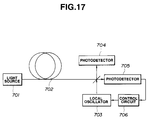
- Fig. 17 is a block diagram illustrating a transmission system for performing coherent optical communication according to the present invention.
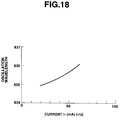
- Fig. 18 is a graph illustrating a wavelength changeable characteristic of a distributed feedback semiconductor laser.
- Fig. 19 is a block diagram illustrating a transmission system for performing wavelength division multiplexing transmission according to an eighth embodiment of the present invention.
- Fig. 20 is a transmission spectrum, illustrating wavelength multiplexed signals according to the present invention.
- Fig. 21 is a view of a ninth embodiment of the present invention, showing an optical node .
- Fig. 22 is a block diagram of an optical local area network (LAN) according to the present invention.
- Fig. 23 is a block diagram of an optical cable television (CATV) system according to the present invention.
- CATV optical cable television
- FIG. 7 shows a two-electrode DFB laser which is used for performing a driving method of the present invention.
- Fig. 9 shows a driving system of the first embodiment.
- reference numeral 101 is an n-type GaAs substrate
- reference numeral 108 is an n-type Al x Ga 1-x As
- a grating g having a pitch of 245 nm and a depth of 100nm is formed on the light guide layer 104, and an antireflection coating 111 is provided on one of light-emerging end faces.
- the p-electrode 109 and the contact layer 106 are each divided into two portions by a space, provided at the device's center as shown in Fig. 7.
- Bias current I 1 is caused to flow through the electrode 109 on the side nearest the antireflection coating 111, and bias current I 2 is caused to flow through the electrode 109 on the other side.
- a high-frequency modulation current ⁇ I 1 is superposed only on the bias current I 1 by a bias T, which is a means for alternating current (AC) coupling, to perform the frequency modulation.
- the modulation characteristic at this time is illustrated in Fig. 8.
- the modulation efficiency remains flat or constant at about 0.6GHz/mA over a range of the modulation frequency from several MHz to several GHz.
- compensation current ⁇ I 2 is superposed on the bias current I 2 by using a structure as shown in Fig. 9.
- a modulation signal from a modulation electric source 409 is divided into two current output portions having a 1:1 ratio by a power divider 408.
- One output is provided to an inverting type wideband video amplifier 406 whose gain and cutoff frequency are respectively approximately 10 and 10GHz.
- the amplified current, ⁇ I 1 is superposed on a DC current I 1 , provided by a DC current source 403 by means of a bias T 402 which is constructed from a solenoid and a capacitor, having component values chosen to provided a low frequency cutoff of about 1kHz.
- the capacitor further allows DC components, such as offsets, to be removed from the amplified current ⁇ I 1 .
- the thus-superposed current (I 1 + ⁇ I 1 ) drives a semiconductor laser 401.
- the laser 401 is depicted by using a pair of diodes.
- the other current output of the power divider 408 is input into a non-inverting type operational amplifier 407 whose gain and cutoff frequency are respectively about 3 and 10MHz.
- its amplified current ⁇ I 2 is superposed on DC current I 2 from a DC current source 405 by a bias T 404, and another superposed current (I 2 + ⁇ I 2 ) also drives the laser 401.
- the output of the modulation electric source 409 is variable, and a modulation index is adjusted by varying the output of modulation source 409.
- the modulation index is a ratio between maximum and minimum current of the superposed modulation current.
- the gain of the inverting wideband video amplifier 406 is fixed at a value of about 10, and the gain of the non-inverting operational amplifier 407 is varied until the desired characteristics are achieved.
- the gain of the non-inverting operational amplifier 407 is preferably about 3.
- the gain values will differ depending on the device structure, material, packaging configuration and the like, and therefore, they need to be adjusted to optimum values for each application.
- the low-frequency band modulation characteristic is highly improved as illustrated in Fig. 10.
- a flat modulation characteristic is obtained over a range down to several kHz.
- the phase difference characteristic exhibits an in-phase response in a range from several kHz to about 1GHz. Consequently, even a simple-structure DFB laser can achieve a frequency modulation with a square wave signal, whose frequency is from several kHz to several GHz, or FSK transmission.
- the wideband video amplifier 406 is preferably an inverting type and the operational amplifier 407 is preferably a non-inverting type in the first embodiment. This is only because an inverting type wideband amplifier has generally superior noise and offset characteristics than other types. However, a non-inverting wide band video amplifier and an inverting operational amplifier may alternatively be used without departing from the invention.
- a two-electrode DFB laser as shown in Fig. 7 is prepared.
- the modulation characteristic is as shown in Fig. 8.
- the effect of heat in a low-frequency band range is reduced compared with the laser as shown in Fig. 1, but yet the desirable flat region extends only down to about several MHz. Therefore, a phase-shifted or anti-phase signal synchronized with the modulation signal is injected through another electrode when the modulation frequency is in a low-frequency (less than several tens MHz) band range.
- the magnitude of the phase-shifted current varies depending on material, structure and packaging configuration of devices.
- This magnitude is adjusted to an optimum value by adjusting the gains of the respective amplifiers 406 and 407 so that the phase difference between the modulation current injected through the first electrode and a light output from the laser ia maintained at zero over a low-frequency band range. Then, the low-frequency characteristic can be extended down to several kHz as shown in Fig. 10.
- Such a means for generating an anti-phase signal can be constructed in various manners. Such means can be readily realized since only a low-frequency band range, extending from about DC to about 10-20 MHz, needs to be considered. One example is shown in Fig. 9.
- a second embodiment of the present invention will be described with reference to Fig. 11.
- a laser device used in connection with this embodiment is substantially the same as the two-electrode DFB laser used in the first embodiment.
- a conventional laser driver integrated circuit (IC) is preferably used as a voltage-current converter, which is a coupling device that can be modulated, to reduce the size of the entire driving system.
- the voltage-current converter supplies driving current by using a voltage signal.
- DC current sources I b1 and I b2 and modulation current sources I p1 and I p2 are connected in a parallel arrangement, and modulation currents ⁇ I 1 and ⁇ I 2 having DC offset currents I 1 and I 2 can be supplied respectively therefrom by inputting thereinto a modulation signal from a modulation signal source 505.
- the modulation index and bias current amount can be controlled on the IC side, respectively, as described above.
- the output of a modulation current source 505 is supplied to the driver ICs 503 and 504.
- the driver IC 503 supplies an in-phase output, which is in-phase with the modulation signal input, to a laser 501 as driving current I 1 + ⁇ I 1 .
- the driver IC 504 supplies an anti-phase output which is anti-phase with the modulation signal input. This can be performed by a single driver IC which can supply in-phase and anti-phase outputs.
- the anti-phase output is input into a low pass filter 502, which has a cutoff frequency of about 10MHz, and the output of the low pass filter 502 is supplied to a laser 501 as driving current of I 2 + ⁇ I 2 .
- the current magnitude ratio between ⁇ I 1 and ⁇ I 2 is made optimum at about 10:3, similar to the first embodiment.
- the driver IC is preferably designed as shown in Fig. 11, wherein the laser 501 is grounded on its upper side to draw current thereinto, so that a high-speed modulation operation can be obtained. Therefore, in this embodiment, the conduction type of the laser 501 is opposite to that shown in Fig. 7. That is, a p-type substrate is used and the electrode is divided into two portions on the side of an n-type electrode.
- the entire system can be made very compact in size, and can be put into a single box as a module. While the lower limit of a low modulation frequency range is limited by the cutoff frequency of the bias T in the first embodiment, there is no lower limit concerning a low modulation frequency range in the second embodiment. As a result, the low modulation frequency characteristic can be further improved, and the modulation frequency characteristic can be flattened over a modulation frequency range between about 100Hz and several GHz.
- NRZ No Return Zero
- the driving circuit of the first embodiment for improving the low modulation frequency range characteristic of a laser includes means for narrowing the spectral line-width of oscillation wavelength of a laser by an electric feedback.
- a period of oscillation wavelength fluctuation is longer than a predetermined value, a general feedback method for narrowing the spectral line-width cannot be applied because the above-discussed phase shift due to the effect of heat occurs.
- This embodiment can cope with such a problem.
- a driving system is shown in Fig. 12.
- a light beam from a semiconductor DFB laser 601 is input into an optical frequency discriminator 610 to convert fluctuation of the wavelength of radiated light beam to fluctuation of a light intensity, and the fluctuation of the light intensity is converted to an electric signal by a photodetector 609.
- a Fabry-Perot etalon whose free spectral range and finesse are respectively 5GHz and 50, is preferably used as the optical frequency discriminator 610.
- a GaAs pin photodiode is preferably employed as the photodetector 609. The electric signal so provided is superposed on injection current into the laser 601.
- the output of photodetector 609 is provided as an input to a power divider 608, in a similar manner as the modulation signal source 409 of the first embodiment, and the feedback control is performed.
- the feedback ratio can be adjusted by varying the gains of amplifiers 606 and 607 and the light power incident on the photodetector 609. In this case, the gains of the amplifiers 606 and 607 are respectively set to about 100 and 30, and an optimum feedback adjustment is achieved with light power in a range between about 10 ⁇ W and about 100 ⁇ W.
- a long optical path length of the feedback system may limit the top of the high modulation frequency band, so the path length is restricted to about 10cm and the frequency, at which a resonance occurs owing to a time delay of the feedback signal, is moved away to 3GHz.
- the spectral line-width is around 15MHz under non-feedback control condition
- the spectral line-width can be narrowed to about 200kHz, i.e. about a hundredth of 15MHz, in this embodiment.
- This level is a practical level for making the laser usable as a light source of coherent optical communications.
- FSK transmissions can be conducted by using the driving system and method of the first or second embodiment.
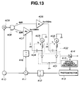
- FIG. 13 A fourth embodiment of the present invention will be described with reference to Figs. 13 and 14.
- the fourth embodiment is different from the first embodiment in the following point.
- Fig. 13 the same reference numerals as those in Fig. 9 designate the same members or devices.
- the gain of amplifier 407 is made variable, and automatically adjusted to suppress the effect of heat in a low modulation frequency band range.
- a sinusoidal wave oscillator 410 outputs two signals of approximately 5kHz.
- One sinusoidal wave signal is input into a modulation electric source 409 and superposed on a modulation signal generated by the modulation electric source 409, and the other signal is mixed, by a balanced modulator 411, with a signal which is produced as follows:
- a portion of the output of a laser 401 is extracted by a beam splitter 414.
- the extracted light is transmitted through a frequency discriminator 415, such as preferably a Fabry-Perot etalon, and converted to an electric signal output by a photodetector 413.
- a signal component of about 5kHz is picked out from the photodetector output signal by a band pass filter 412.
- the other oscillator signal is mixed, by the balanced modulator 411, with the approximately 5kHz signal from the band pass filter 412.
- a DC component of the mixed output from the balanced modulator 411 is selected out by a low pass filter 416, and provided as a gain control signal to amplifier 407 which is automatically gain controlled by this DC signal. This principle will be described with reference to Fig. 14.
- the frequency modulation occurs substantially only due to the effect of heat.
- an oscillation frequency fluctuation ⁇ f 2 caused by the effect of heat due to an injected current ⁇ I 2 is smaller than an oscillation frequency fluctuation ⁇ f 1 caused by the effect of heat due to an injected current ⁇ I 1 , as shown in a portion (a) of Fig. 14, the frequency fluctuation of output light is in-phase with ⁇ f 1 or anti-phase with ⁇ I 1 .
- the frequency fluctuation of output light is in-phase with ⁇ I 1 , or anti-phase with ⁇ f 1 .
- the oscillation frequency fluctuation ⁇ f 2 is substantially equal to the frequency fluctuation ⁇ f 1 as shown in a portion (b) of Fig. 14, no output oscillation frequency fluctuation exists due to mutual elimination.
- a positive DC output is obtained from balanced modulator 411, when the photodetector output is in-phase with the sinusoidal wave signal or anti-phase with ⁇ I 1 which is provided by the inverting amplifier 406, as shown in the portion (a) of Fig. 14.
- a negative DC output is obtained from balanced modulator 411. If no frequency fluctuation exists as shown in the portion (b) of Fig. 14, the mixed output is zero. The case where the output is zero as shown in the portion (b) of Fig.
- the sinusoidal wave component of 5kHz which is used for the above-discussed automatic gain control, is removed at the signal receiver side.
- the frequency of the sinusoidal wave is preferably 5kHz, which is cosen because its frequency value is low enough to cause frequency modulation solely due to the effect of heat and large enough to enable transmission through a bias T without attenuation due to a low cutoff frequency.
- a low-frequency signal for which the effect of heat is dominant, is superposed on each current injected into the laser.
- a feedback control is performed.
- Two electrodes are respectively modulated by low-frequency signals, such as sinusoidal wave signals of about 100Hz, for which the effect of heat is dominant, with those signals having the same amplitude and being in an anti-phase with each other, a portion of output signal from the laser is picked out, only a component of about 100Hz is selected by a band pass filter, and the selected component is combined with the sinusoidal wave signal of 100Hz which modulates the laser.
- a positive, zero or negative DC output can be obtained depending on the magnitude of modulation factor due to the effect of heat at regions of the two electrodes.
- the feedback control is performed based on that DC output, and the modulation current amplitude provided at one of the two electrodes is adjusted by a gain controlled amplifier or attenuator, operating in response to the DC signal.
- a fifth embodiment of the present invention will be described with reference to Fig. 15.
- the fifth embodiment is different from the second embodiment in the following point.
- the current ratio between and ⁇ I 1 ⁇ I 2 is made variable, by adjusting the modulation current amplitude of driver IC 504, in the same manner as the fourth embodiment.
- the modulation current amplitude I p of the driver IC 504 is automatically controlled by a mixed output of a low pass filter 511 which is produced by the superposition of a sinusoidal wave signal of 100Hz from a sinusoidal wave oscillator 506 and an output from a band pass filter 508 derived from a laser 501 in the same manner as the fourth embodiment.
- the frequency of the sinusoidal wave signal is preferably as low as possible to increase the continuity of NRZ signal.
- this frequency is set at about 100Hz because there is no limiting low-frequency cutoff due to a bias T such as was described in the fourth embodiment.
- reference numeral 507 designates a balanced modulator
- reference numeral 509 designates a photodetector
- reference numeral 510 designates an optical frequency discriminator. The operation of this embodiment is substantially the same as that of the fourth embodiment.
- a sixth embodiment of the present invention will be described with reference to Fig. 16.
- the sixth embodiment is different from the third embodiment in the following point.
- An electric signal detected by a photodetector 609 is input into a band elimination filter or trap circuit 612, whose output is superposed on the injection current into a laser 601 in a manner similar to the fourth embodiment to provide feedback control.
- the gain of the amplifier 607 is variable.
- the gain of amplifier 607 is rendered optimum by the antomatic control in the same manner as the fourth embodiment.
- a 5kHz signal, from a sinusoidal wave oscillator 611 is input into each of amplifiers 606 and 607.
- the output of photodetector 609 is further input into a band pass filter 613, whose output is mixed with the sinusoidal wave provided by balanced modulator 614.
- the mixed signal is transmitted through a low pass filter 615, and provided as a gain control signal which automatically controls the gain of the amplifier 607 to cancel the effect of heat mentioned above. It is necessary to prevent the occurrence of oscillation which would be caused when a signal, that is produced from the fluctuation of oscillation wavelength due to the sinusoidal wave signal, would be fed back without any change.
- the band elimination filter 612 serves to remove that component of frequency (the sinusoidal wave oscillation frequency) which will cause the oscillation.
- Fig. 17 shows a structure in which an optical transmission system is assembled including a light source which is driven by the above-discussed driving method of the first embodiment, the combination of first and third embodiments, the fourth embodiment, the combination of fourth and sixth embodiments or the like.
- a light beam emitted from a light source 701 is coupled to a single mode optical fiber 702 to be transmitted therethrough.
- a laser 703 is provided as a local oscillator which emits an oscillating light beam having the same wavelength as that of the light source 701, and an optical beat signal is generated by using the light beams from the both lasers 701 and 703.
- the beat signal is detected by a photodetector 705 using a delayed detection method.
- the oscillation wavelength of the laser 703 is stabilized by a conventional phase-locked loop (PLL) control circuit 706, using a signal created from the beat signal detected by a photodetector 705 as a control source.
- PLL phase-locked loop
- the tunable characteristic or wavelength-changeable characteristic of a laser is utilized to perform wavelength or frequency division multiplexing transmissions.
- the oscillation wavelength can be changed by controlling the magnitudes of current injected through the respective electrodes.
- the tunable characteristic is illustrated in Fig. 18.
- this property is utilized and a center of the oscillation wavelength spectrum is determined by controlling the bias current.
- Frequency modulation is conducted as described in the first embodiment or the like.
- the oscillation spectral line-width also may be narrowed as described in the third embodiment, the combination of first and third embodiments, the sixth embodiment, or the combination of fourth and sixth embodiments.
- FIG. 19 a method for performing wavelength division multiplexing communication by using the driving method of this embodiment is illustrated.
- reference numeral 901 is a light source for optical communications, which is modulated by FSK system using the present invention.
- the oscillation wavelength can be changed in a range having a width of 1nm as described above.
- a frequency deviation amount of 5GHz of FSK system can be obtained by setting the modulation current amplitude to about 8.3mA. Therefore, when channels are arranged at intervals of about 10GHz or 0.02nm to perform the wavelength multiplexing, crosstalk among adajacent channels can be eliminated.
- a light beam emitted from the light source 901 is coupled to a single mode optical fiber 902 to be transmitted therethrough.
- the signal light transmitted through the optical fiber 902 is received by a receiver apparatus.
- light of a desired wavelength is selectively demultiplexed by an optical filter 903, and the signal is detected by a photodetector 904.
- a laser having the same structure as that of DFB laser of the first embodiment is used as the optical filter 903, and bias current having a magnitude below its threshold is injected thereinto.
- the 10dB-down transmission width of the filter 903 is approximately 10GHz or 0.02nm, and thus this filter 903 has sufficient bandwidth characteristic to attain the wavelength multiplexing having the intervals of 0.02nm as descrived above.
- the transmission characteristic of the filter 903 is utilized. As shown in Fig. 20, when the peak transmission wavelength of the filter 903 is tuned to a mark frequency (corresponding to a "1" of an FSK signal) of a desired channel, e.g. CH2, in the wavelength multiplexed signals, "1" and "0" can be detected at an extinction ratio of 10dB after transmission through the filter 903 since a space frequency (corresponding to a "0" of an FSK signal) is remote from the mark frequency by the frequency deviation amount of 5GHz as described above.
- a mark frequency corresponding to a "1" of an FSK signal
- a desired channel e.g. CH2
- optical filter 903 As an alternative to optical filter 903, other filters such as a Mach-Zehnder type filter and a fiber Fabry-Perot type filter, may be used. Furthermore, in this embodiment, a single light source and a single receiver apparatus are preferred, but a plurality of light sources and a plurality of receiver apparatuses respectively connected by optical couplers or the like may be used for optical communications.
- a receiver for wavelength multiplexed signals may be a coherent system as described in the seventh embodiment, other than the method of this embodiment.
- Fig. 21 shows an opto-electric conversion unit (node) which is connected to each terminal when a driving method of a light source for optical communications of the present invention and an optical communication system using this driving method are applied to a wavelength or frequency division multiplexing optical LAN system.
- Fig. 22 shows an example of an optical LAN system in which the node is utilized.
- An optical signal is taken into the node through an optical fiber 1001 externally connected thereto, and a portion of the signal is caused to enter a receiving device 1003 having a tunable filter such as filter 903 of Fig. 19, discussed above, through a branching device 1002.
- a receiving device 1003 having a tunable filter such as filter 903 of Fig. 19, discussed above, through a branching device 1002.
- An alternative receiving method may use coherent system as discussed in reference with Fig. 17 above, and in this case a local oscillation laser is provided in place of the optical filter.
- a plurality of tunable DFB lasers and a plurality of tunable optical filters may respectively be arranged so that the changeable wavelength range can be widened.
- the optical LAN system shown in Fig. 22 is a bus type network, and nodes 1011, 1012, 1013 are connected along A and B directions so that multiple terminals 1021, 1022, 1023 and centers, which constitute a network, can be provided.
- nodes 1011, 1012, 1013 are connected along A and B directions so that multiple terminals 1021, 1022, 1023 and centers, which constitute a network, can be provided.
- two nodes may be connected to each terminal to build two transmission lines, so that a bidirectional transmission is possible by DQDB system or the like.
- a high-density wavelength or frequency division multiplexing transmission network which has a wavelength multiplicity of 50, can be constructed as described above.
- a loop type network can be constructed by connecting A and B in Fig. 22, and a star type network and a compound-configuration type network may be established.
- An optical CATV as shown in Fig. 23, can be constructed using the apparatus and optical communication system of the present invention.
- a tunable laser is modulated in accord with the invention as described above, and a wavelength multiplexing light source is constructed also in accord with the invention.
- a receiver apparatus having a tunable filter such as described in connection with Fig. 19, is used.
- a bidirectional CATV is possible in the following manner.
- the subscriber 1033 has an external modulator (an example of simple bidirectional optical CATV, see, for example, Ishikawa and Furuta "LiNbO 3 Optical Wavelength Modulator For Bi-directional Transmission in Optical CATV Subscriber Systems", OCS 91-82 1991), and a signal from the subscriber 1033 is received as a reflected light (reflected light of a signal light transmitted to the subscriber 1033) from its external modulator.
- a star type network as shown in Fig. 23 is constructed, and highly improved functions of services can be obtained.
- a modulation frequency band range on a low-frequency side can be greatly expanded when a semiconductor laser is frequency-modulated, and hence a high-speed transmission becomes possible. In particular cases, this can be achieved irrespective of changes in laser's packaging configuration, environment and the like.
- a band range can be widened when an oscillation spectral line-width is narrowed by an electric feedback method, so that a spectral line width, which is narrower than that of a conventional one, can readily be attained.
- a light source which is suitable for a coherent optical communication, can be provided, for example.
- a driving method of the present invention drives a semiconductor laser which is provided with at least first and second electrodes through each of which current is injected into the semiconductor laser. Varying current is injected through the first electrode when the frequency of the varying current is in a high frequency band. Varying current is injected through the first electrode while phase-shifted current, whose phase is shifted relative to the varying current, is injected through the second electrode, when the frequency of the varying current is in a low frequency band which is lower than the frequency of the high frequency band. Feedback-control may be performed for controlling a ratio between amplitudes of the modulation current and the phase-shifted current based on a light output from the semiconductor laser.
- the varying current includes at least modulation current modulated according to a predetermined signal or negative feedback current produced by an electric signal obtained by detecting fluctuation of oscillation wavelength of a light output from the semiconductor laser.
Landscapes
- Physics & Mathematics (AREA)
- Condensed Matter Physics & Semiconductors (AREA)
- General Physics & Mathematics (AREA)
- Electromagnetism (AREA)
- Optics & Photonics (AREA)
- Semiconductor Lasers (AREA)
- Optical Communication System (AREA)
Claims (53)
- Ansteuerverfahren zur Ansteuerung eines Halbleiterlasers, der mit wenigstens einer ersten und einer zweiten Elektrode versehen ist, durch die Strom in den Halbleiterlaser eingespeist wird, mit den Verfahrensschritten:Einspeisen eines ersten Stromes variierender Frequenz durch die erste Elektrode, wenn die Frequenz des ersten Stromes in einem ersten Frequenzband liegt; undEinspeisen des ersten Stromes durch die erste Elektrode, während gegenüber dem ersten Strom phasenverschobener Strom durch die zweite Elektrode eingespeist wird, wenn die Frequenz des ersten Stromes in einem zweiten Frequenzband unter dem ersten liegt;wobei der phasenverschobene Strom nicht durch die zweite Elektrode eingespeist wird, wenn die Frequenz des ersten Stromes im ersten Frequenzband liegt.
- Ansteuerverfahren nach Anspruch 1, bei dem der phasenverschobene Strom ein gegenphasiger Strom ist.
- Ansteuerverfahren nach Anspruch 1, bei dem das zweite Frequenzband Frequenzen unter etwa 10 MHz umfaßt.
- Ansteuerverfahren nach Anspruch 1, bei dem der erste Strom wenigstens einen gemäß einem vorbestimmten Signal modulierten Modulationsstrom enthält.
- Ansteuerverfahren nach Anspruch 4, bei dem die Modulationsamplitude des phasenverschobenen Stromes, der durch die zweite Elektrode eingespeist wird, so eingestellt ist, daß keine Phasendifferenz zwischen dem durch die erste Elektrode eingespeisten Modulationsstrom und einem vom Halbleiterlaser emittierten Lichtfrequenz- Modulationssignal entsteht.
- Ansteuerverfahren nach Anspruch 4, mit dem weiteren Verfahrensschritt der Rückkopplungssteuerung eines Verhältnisses zwischen Amplituden des Modulationsstroms und dem phasenverschobenen Strom auf der Grundlage eines Lichtausgangssignals aus dem Halbleiterlaser.
- Ansteuerverfahren nach Anspruch 6, bei dem die Rückkopplungssteuerung so ausgeführt wird, daß eine Phasendifferenz zwischen dem durch die erste Elektrode eingespeisten Modulationsstrom und einem vom Halbleiterlaser emittierten Lichtfrequenz- Modulationssignal auf einer über ein breites Modulationsband im wesentlichen konstanten Größe beibehalten wird.
- Ansteuerverfahren nach Anspruch 6, bei dem die Rückkopplungssteuerung ausgeführt wird durch: Überlagern eines Sinuswellensignals, dessen Frequenz niedriger als die Modulationsfrequenz ist, mit sowohl dem Modulationsstrom als auch dem phasenverschobenen Strom, Umsetzten von Fluktuationen eines vom Halbleiterlaser emittierten Lichtfrequenz-Modulationssignals, der durch das Sinuswellensignal zur Fluktuation der Lichtintensität veranlaßt wird, Feststellen der Fluktuation der Lichtintensität, Multiplizieren der festgestellten Fluktuation der Lichtintensität durch das Sinuswellensignal, um ein Produktsignal zu liefern, Auswahl einer Niederfrequenzkomponente aus dem Produktsignal, deren Frequenz niedriger als die Frequenz des Sinuswellensignals ist, und Steuern der Amplitude wenigstens eines der Ströme, die den Modulationsstrom und den phasenverschobenen Strom umfassen, auf der Grundlage der ausgewählten Niederfrequenzkomponente.
- Ansteuerverfahren nach Anspruch 1, bei dem der erste Strom wenigstens einen negativen Rückkopplungsstrom durch ein elektrisches Signal enthält, das durch Feststellung der Fluktuation der Schwingungswellenlänge eines Lichtausgangssignals aus dem Halbleiterlaser gewonnen wird.
- Ansteuerverfahren nach Anspruch 9, bei dem die Amplitude des durch die zweite Elektrode eingespeisten phasenverschobenen Stroms so eingestellt wird, daß keine Phasendifferenz zwischen dem durch die erste Elektrode eingespeisten negativen Rückkopplungsstrom und der Fluktuation der Schwingungswellenlänge des Lichtausgangssignals vom Halbleiterlaser verursacht wird, wobei die Fluktuation durch den in den Halbleiterlaser eingespeisten negativen Rückkopplungsstrom und den phasenverschobenen Strom verursacht wird.
- Ansteuerverfahren nach Anspruch 9, mit dem weiteren Verfahrensschritt einer Rückkopplungssteuerung eines Verhältnisses zwischen Amplituden des negativen Rückkopplungsstromes und dem phasenverschobenen Strom auf der Grundlage des Lichtausgangssignals vom Halbleiterlaser.
- Ansteuerverfahren nach Anspruch 11, bei dem die Rückkopplungssteuerung so ausgeführt wird, daß eine Phasendifferenz zwischen dem durch die erste Elektrode eingespeisten negativen Rückkopplungsstrom und der Fluktuation der Lichtfrequenz des vom Halbleiterlaser emittierten Lichtausgangssignals auf einer im wesentlichen konstanten Größe über ein breites Band beibehalten wird, wobei die Fluktuation durch den negativen Rückkopplungsstrom und den in den Halbleiterlaser eingespeisten phasenverschobenen Strom verursacht wird.
- Ansteuerverfahren nach Anspruch 11, bei dem die Rückkopplungssteuerung ausgeführt wird durch: Überlagern eines Sinuswellensignals, dessen Frequenz niedriger als die Frequenz des negativen Rückkopplungsstromes ist, mit sowohl dem negativen Rückkopplungsstrom als auch dem phasenverschobenen Strom, Umsetzen der durch das Sinuswellensignal verursachten Fluktuation der Licht frequenz des vom Halbleiterlaser emittierten abgegebenen Lichts in die Fluktuation der Lichtintensität, Feststellen der Fluktuation der Lichtintensität, Multiplizieren der festgestellten Fluktuation der Lichtintensität mit dem Sinuswellensignal, um ein Produktsignal zu liefern, Auswahl einer Niederfrequenzkomponente aus dem Produktsignal, deren Frequenz niedriger als die Frequenz des Sinuswellensignals ist, und Steuern eines Verhältnisses zwischen Amplituden des negativen Rückkopplungsstroms und des phasenverschobenen Stroms auf der Grundlage der ausgewählten niederfrequenten Komponente.
- Ansteuerverfahren nach einem der Ansprüche 1 bis 13, bei dem der Halbleiterlaser aktive Bereiche in einem Bereich enthält, in den der Strom durch die erste Elektrode eingespeist wird, und einen Bereich, in den der Strom durch die zweite Elektrode eingespeist wird.
- Ansteuergerät zur Ansteuerung eines Halbleiterlasers, der mit wenigstens einer ersten und einer zweiten Elektrode versehen ist, durch die in den Halbleiterlaser ein Strom veränderbarer Frequenz eingespeist wird, mit:
einer Steuerung (402, 403, 404, 405,406, 407; 502, 503, 504; 602, 603, 604, 605, 606, 607) zum Steuern der Einspeisung eines Stromes in eine erste und eine zweite Elektrode, dessen Frequenz verändert wird, wobei die Steuerung den eingespeisten Strom in die erste und zweite Elektrode gemäß dem Umstand steuert, ob die Frequenz des Stromes in einem ersten Frequenzband oder in einem zweiten Frequenzband liegt, das tiefer als das erste Frequenzband ist, in der Weise, daß ein erster Strom durch die erste Elektrode eingespeist wird, wenn die Frequenz des Stromes im zweiten Frequenzband liegt, und phasenverschobener Strom, dessen Phase bezüglich des ersten Stromes verschoben ist, durch die zweite Elektrode eingespeist wird, und wenn die Frequenz des Stromes im ersten Frequenzband liegt, wird der erste Strom durch die erste Elektrode eingespeist, und der phasenverschobene Strom wird nicht durch die zweite Elektrode eingespeist. - Ansteuergerät nach Anspruch 15, bei dem der phasenverschobene Strom gegenphasig zum ersten Strom ist.
- Ansteuergerät nach Anspruch 15, dessen zweites Frequenzband Frequenzen unter etwa 10 MHz enthält.
- Ansteuergerät nach Anspruch 15, bei dem der Strom wenigstens einen gemäß einem vorbestimmten Signal modulierten Modulationsstrom enthält.
- Ansteuergerät nach Anspruch 18, das des weiteren ausgestattet ist mit einem Signalgenerator (408, 409; 501; 608) zur Erzeugung zweier Signale, die jeweils wenigstens den Modulationsstrom enthalten, und wobei die Steuerung ein erstes und ein zweites Einspeisemittel enthält, wobei das erste Einspeisemittel sowohl einen ersten Verstärker (406; 606) mit einer Grenzfrequenz oberhalb mehrerer GHz enthält, der eines der beiden Signale empfängt, um ein erstes Ausgangssignal zu liefern, als auch erste Einkoppelmittel (402; 602) zum Abschneiden einer Gleichstromkomponente des ersten Ausgangssignals und zum Überlagern des solchermaßen abgeschnittenen ersten Ausgangssignals mit einem ersten Vorstrom und zur Einspeisung des überlagerten Stromes durch die erste Elektrode in den Halbleiterlaser enthält, und wobei das zweite Einspeisemittel sowohl einen zweiten Verstärker (407; 607) enthält, dessen Grenzfrequenz unter der des ersten Verstärkers liegt, wobei der zweite Verstärker das andere der beiden Signale empfängt, um ein zweites, zum ersten gegenphasiges Ausgangssignal zu liefern, als auch zweite Einkoppelmittel (404; 604) zum Abschneiden einer Gleichstromkomponente des zweiten Ausgangssignals und zur Überlagerung des solchermaßen abgeschnittenen zweiten Ausgangssignals mit einem zweiten Vorstrom und zur Einspeisung des überlagerten Stroms durch die zweite Elektrode in den Halbleiterlaser.
- Ansteuergerät nach Anspruch 19, bei dem die Grenzfrequenz des zweiten Verstärkers (404; 604) etwa 10 MHz beträgt.
- Ansteuergerät nach Anspruch 19, dessen einer der ersten und zweiten Verstärker ein invertierender Verstärker und dessen anderer ein nichtinvertierenden Verstärker ist.
- Ansteuergerät nach Anspruch 19, dessen Signalerzeuger über eine elektrische Modulationsquelle (409) zur Lieferung eines Modulationsstroms und über einen Teiler (408) zur Aufteilung des Modulationsstroms in zwei Signale verfügt.
- Ansteuergerät nach Anspruch 22, bei dem ein Verhältnis zwischen Amplituden wenigstens der Modulationssignale des ersten und zweiten Ausgangssignals durch Ändern eines Verhältnisses zwischen den Verstärkungen des ersten und zweiten Verstärkers einstellbar ist.
- Ansteuergerät nach Anspruch 19, dessen Signalerzeuger über Mittel (408, 409, 410) zur Erzeugung zweier Signale verfügt, von denen jedes über ein Modulationsstrom- und ein Sinuswellensignal verfügt, das dem Modulationsstrom überlagert ist, und dessen Frequenz niedriger als die Frequenz des Modulationsstroms ist.
- Ansteuergerät nach Anspruch 24, das des weiteren ausgestattet ist mit:einem Aufspalter (414) zum Abzweigen eines Teils eines Lichtausgangssignals vom Halbleiterlaser;einem Lichtfrequenzdiskriminator (415) zur Umwandlung der Fluktuation der Lichtfrequenz des Lichtausgangssignals vom Halbleiterlaser in Lichtintensitätsfluktuation zur Lieferung eines Fluktuationsausgangssignals;einem Photodetektor (413) zur Feststellung des Fluktuationsausgangssignal aus dem Lichtfrequenzdiskriminator zur Lieferung eines elektrischen Signals;einem Bandpaßfilter (412) zur Auswahl einer Frequenzkomponente aus dem elektrischen Signal vom Photodetektor, deren Frequenz im wesentlichen dieselbe wie die Frequenz des Sinuswellensignals ist; einem Multiplizierer (411) zur Multiplikation des Sinuswellensignals mit der Komponente des vom Bandpaßfilter ausgewählten elektrischen Signals, um ein elektrisches Produktsignal zu liefern;einem Tiefpaßfilter (416) zum Auslesen einer Komponente aus dem elektrischen Produktsignal, deren Frequenz niedriger als die Frequenz des Sinuswellensignals ist; und mitJustiermitteln zur Einstellung eines Verhältnisses zwischen Verstärkungen des ersten und des zweiten Verstärkers auf der Grundlage der von dem Tiefpaßfilter aufgenommenen Komponente.
- Ansteuergerät nach Anspruch 18, das des weiteren ausgestattet ist mit Signalerzeugern (501) zur Erzeugung zweier Signale, von denen jedes wenigstens den Modulationsstrom enthält, und wobei das Steuermittel ein erstes und ein zweites Einspeisemittel enthält, wobei das erste Einspeisemittel einen ersten Spannung- Strom- Wandler (504) enthält, der ein gegenphasiges Ausgangssignal liefert, wobei der erste Spannung-Strom- Wandler eines der beiden Signale zusammen mit einem ersten Vorstrom durch die erste Elektrode in den Halbleiterlaser als gegenphasiges Ausgangssignal einspeist, wobei das zweite Einspeisemittel einen zweiten Spannung- Strom-Wandler (503) enthält, um ein mitphasiges Ausgangssignal zu liefern, wobei der zweite Spannung- Strom- Wandler das andere der beiden Signale zusammen mit einem zweiten Vorstrom in den Halbleiterlaser durch die zweite Elektrode als mitphasiges Ausgangssignal einspeist, und wobei entweder das erste oder das zweite Einspeisemittel des weiteren ein erstes Tiefpaßfilter (502) enthält, das zwischen dem ersten oder zweiten Spannung-Strom- Wandler und dem Halbleiterlaser angeordnet ist.
- Ansteuergerät nach Anspruch 26, wobei die Grenzfrequenz des ersten Tiefpaßfilters (502) in etwa 10 MHz beträgt.
- Ansteuergerät nach Anspruch 26, dessen Signalerzeuger über eine elektrische Modulationsquelle (505) verfügt, die einen Modulationsstrom liefert, und über Teilmittel zur Aufteilung des Modulationsstrom in zwei Signale.
- Ansteuergerät nach Anspruch 28, bei dem ein Verhältnis zwischen Modulationsamplituden der gegenphasigen und mitphasigen Ausgangssignale durch Änderung eines Verhältnisses zwischen den Verstärkungen des ersten und zweiten Spannung-Strom-Wandlers einstellbar ist.
- Ansteuergerät nach Anspruch 26, dessen Signalerzeuger über Mittel (505, 506) zur Erzeugung zweier Signale verfügt, von denen jedes ein Modulationsstrom- und ein Sinuswellensignal enthält, das dem Modulationsstrom überlagert ist, und dessen Frequenz niedriger als die Frequenz des Modulationsstroms ist.
- Ansteuergerät nach Anspruch 30, das des weiteren ausgestattet mit:einem Abzweiger zum Abzweigen eines Teils eines Lichtausgangssignals vom Halbleiterlaser;einem Lichtfrequenzdiskriminator (510) zur Umwandlung der Fluktuation der Lichtfrequenz des Lichtausgangssignals vom Halbleiterlaser in Lichtintensitätsfluktuation zur Lieferung eines Fluktuationsausgangssignals;einem Photodetektor (509) zur Feststellung des Fluktuationsausgangssignals aus dem Frequenzdiskriminator zur Lieferung eines elektrischen Signals;einem Bandpaßfilter (508) zur Auswahl einer Komponente aus dem elektrischen Signal vom Photodetektor, deren Frequenz im wesentlichen dieselbe wie die Frequenz des Sinuswellensignals ist;einem Multiplizierer (507) zur Multiplikation des Sinuswellensignals mit der Komponente des vom Bandpaßfilter ausgewählten elektrischen Signals, um ein elektrisches Produktsignal zu liefern;einem zweiten Tiefpaßfilter (511) zum Auslesen einer Komponente aus dem elektrischen Produktsignal, deren Frequenz niedriger als die Frequenz des Sinuswellensignals ist; und miteinem Justiermittel zur Einstellung eines Verhältnisses zwischen der Verstärkung des ersten und des zweiten Spannung-Strom- Wandlers auf der Grundlage der vom zweiten Tiefpaßfilter ausgelesenen Komponente.
- Ansteuergerät nach Anspruch 15, das des weiteren ausgestattet ist mit einem Signalerzeuger zur Erzeugung zweier Signale, dessen Steuermittel über ein erstes und ein zweites Einspeisemittel verfügt, wobei das erste Einspeisemittel sowohl einen ersten Verstärker (606) mit einer Grenzfrequenz oberhalb mehrerer GHz enthält, der eines der beiden Signale empfängt, um ein erstes Ausgangssignal zu liefern, als auch erste Einkoppelmittel (602) zum Abschneiden einer Gleichstromkomponente des ersten Ausgangssignals und zum Überlagern des solchermaßen abgeschnittenen Ausgangssignals mit einem ersten Vorstrom und zur Einspeisung des überlagerten Stromes durch die erste Elektrode in den Halbleiterlaser enthält, und wobei das zweite Einspeisemittel sowohl einen zweiten Verstärker (607) enthält, dessen Grenzfrequenz unter der des ersten Verstärkers liegt, wobei der zweite Verstärker das andere der beiden Signale empfängt, um ein zweites zum ersten Ausgangssignal gegenphasiges Ausgangssignal zu liefern, als auch zweite Einkoppelmittel (602) zum Abschneiden einer Gleichstromkomponente des zweiten Ausgangssignals und zur Überlagerung des solchermaßen abgeschnittenen Ausgangssignals mit einem zweiten Vorstrom und zur Einspeisung des Überlagerten Stroms in den Halbleiterlaser durch die zweite Elektrode enthält.
- Ansteuergerät nach Anspruch 32, bei dem Grenzfrequenz des zweiten Verstärkers (607) etwa 10 MHz beträgt.
- Ansteuergerät nach Anspruch 32, bei dem der erste Verstärker und der zweite Verstärker ein invertierender Verstärker ist, und bei dem der andere ein nichtinvertierender Verstärker ist.
- Ansteuergerät nach Anspruch 32, dessen Signalerzeuger ausgestattet ist mit: einem Aufspalter zur Abzweigen eines Teils eines Lichtausgangssignals aus dem Halbleiterlaser, einem Frequenzdiskriminator (610) zur Feststellung der Fluktuation der Schwingungswellenlänge des Lichtausgangssignals vom Halbleiterlaser, einem Photodetektor (609) zur Feststellung des durch den Frequenzdiskriminator übertragenen Lichts zur Lieferung eines Signals und Aufteilmittel (608) zum Aufteilen des vom Photodetektor gelieferten Signals in zwei Signale.
- Ansteuergerät nach Anspruch 35, bei dem ein Verhältnis zwischen Modulationsamplituden des ersten und zweiten Ausgangssignals durch Änderung des Verhältnisses der Verstärkungen des ersten zum zweiten Verstärker einstellbar ist.
- Ansteuergerät nach Anspruch 32, dessen Signalerzeuger über Mittel 611 verfügt, die zwei zueinander gleichphasige Sinuswellensignale erzeugen.
- Ansteuergerät nach Anspruch 37, das des weiteren ausgestattet ist mit:einem Aufspalter zur Abzweigen eines Teils eines Lichtausgangssignals vom Halbleiterlaser;einem Frequenzdiskriminator (610) zur Feststellung der Fluktuation der Schwingungswellenlängen des Lichtausgangssignals vom Halbleiterlaser;einem Photodetektor (609) zur Feststellung des durch den Frequenzdiskriminator übertragenen Lichts zur Lieferung eines Signals;einem Überlagerungsmittel (608) zur Überlagerung von durch Beseitigung einer Frequenzkomponente des Sinuswellensignals aus dem Signal vom Photodetektor erzeugten Signalen mit den jeweiligen Sinuswellensignalen, um jeweilige überlagerte Signale in den ersten bzw. zweiten Verstärker zu liefern;einem Bandpaßfilter (613) zur Auswahl einer Komponente aus dem Signal vom Photodetektor, deren Frequenz nahe an der Frequenz des Sinuswellensignals liegt;einem Multiplizierer (614) zur Multiplikation des Sinuswellensignals mit einer Komponente des vom Bandpaßfilter ausgewählten Signals, um ein elektrische Produktsignal zu liefern;einem Tiefpaßfilter (615) zum Auslesen einer Komponente aus dem elektrischen Produktsignal, deren Frequenz niedriger als die des Sinuswellensignals ist; und mitJustiermitteln zur Einstellung eines Verhältnisses zwischen Verstärkungen des ersten und zweiten Vestärkers auf der Grundlage der vom Tiefpaßfilter ausgelesenen Signalkomponente.
- Ansteuergerät nach Anspruch 15, das des weiteren ausgestattet ist mit einem Signalgenerator zur Erzeugung zweier Signale, wobei das Steuermittel über ein erstes und ein zweites Einspeisemittel verfügt, wobei das erste Einspeisemittel einen ersten Spannung- Strom- Wandler zur Lieferung eines gegenphasigen Ausgangssignals enthält, wobei der erste Spannung- Strom- Wandler eines der beiden Signale kombiniert mit einem ersten Vorstrom in den Halbleiterlaser durch die erste Elektrode als gegenphasiges Ausgangssignal einspeist, wobei das zweite Einspeisemittel einen zweiten Spannung- Strom-Wandler zur Lieferung eines mitphasigen Ausgangssignals enthält, wobei der zweite Spannung- Strom-Wandler das andere der beiden Signale kombiniert mit einem zweiten Vorstrom in den Halbleiterlaser durch die zweite Elektrode als mitphasiges Ausgangssignal einspeist, und wobei das erste oder zweite Einspeisemittel des weiteren über ein erstes Tiefpaßfilter verfügt, das zwischen dem ersten und zweiten Spannung- Strom-Wandler des Halbleiterlasers geschaltet ist.
- Ansteuergerät nach Anspruch 39, bei dem die Grenzfrequenz des ersten Tiefpaßfilters etwa 10 MHz beträgt.
- Ansteuergerät nach Anspruch 39, dessen Signalerzeuger ausgestattet ist mit: einem Aufspalter zum Abzweigen eines Teils eines Lichtausgangssignals aus dem Halbleiterlaser, einem Frequenzdiskriminator zur Feststellung der Fluktuation der Schwingungswellenlänge des Lichtausgangssignals aus dem Halbleiterlaser, einem Photodetektor zur Feststellung des durch den Frequenzdiskriminator übertragenen Lichtsignals zur Lieferung eines Signals und mit Aufteilmitteln zum Aufteilen des vom Photodetektor gelieferten Signals in zwei Signale.
- Ansteuergerät nach Anspruch 41, bei dem ein Verhältnis zwischen Modulationsamplituden des gegenphasigen und mitphasigen Ausgangssignals durch Änderung eines Verhältnisses zwischen der Verstärkung des ersten und zweiten Spannung- Strom- Wandlers einstellbar ist.
- Ansteuergerät nach Anspruch 39, dessen Signalerzeuger über Mittel zur Erzeugung zweier Sinuswellensignale verfügt, die miteinander in Phase sind.
- Ansteuergerät nach Anspruch 43, das des weiteren ausgestattet ist mit:einem Aufspalter zum Abzweigen eines Teils eines Lichtausgangssignals aus dem Halbleiterlaser;einem Frequenzdiskriminator zur Feststellung der Fluktuation der Schwingungswellenlänge des Lichtausgangssignals aus dem Halbleiterlaser;einem Photodetektor zur Feststellung des durch den Frequenzdiskriminator übertragenen Lichts zur Lieferung eines Signals;Überlagerungsmitteln zur Überlagerung von Signalen, die durch Beseitigung einer Frequenzkomponente des Sinuswellensignals aus dem Signal vom Photodetektor jeweils bezüglich der beiden Sinuswellensignale erzeugt werden, um jeweilige überlagerte Signale in den ersten und zweiten Spannung- Strom- Wandler zu liefern;einem Bandpaßfilter zur Auswahl einer Komponente aus dem Signal vom Photodetektor, deren Frequenz nahe an der Frequenz des Sinuswellensignals liegt;einem Multiplizierer zum Multiplizieren des Sinuswellensignals mit einer Komponente des vom Bandpaßfilter ausgewählten Signals zur Lieferung eines elektrischen Produktsignals;einem zweiten Tiefpaßfilter zur Auswahl einer Komponente aus dem elektrischen Produktsignal, deren Frequenz niedriger als die Frequenz des Sinuswellensignals ist; und mitJustiermitteln zum Einstellen eines Verhältnisses zwischen der Verstärkung des ersten und zweiten Spannung- Strom- Wandlers auf der Grundlage der vom zweiten Tiefpaßfilter herausgetrennten Komponente.
- Ansteuergerät nach einem der Ansprüche 14 bis 44, dessen Halbleiterlaser aktive Zonen in einer Zone enthält, in die Strom von der ersten Elektrode eingespeist wird, und eine Zone, in die Strom von der zweiten Elektrode eingespeist wird.
- Ansteuerverfahren nach Anspruch 9 oder 11, bei dem der erste Strom und der phasenverschobenen Strom des weiteren einen gegenphasigen Modulationsstrom und eine Modulationsamplitude enthalten, von denen wenigstens eine eingestellbar ist, um den Halbleiterlaser in seiner Frequenz zu modulieren.
- Ansteuerverfahren nach Anspruch 46, bei dem die Frequenzmodulation eine Frequenzumtastung ist, bei der Digitalsignale die Frequenzmodulation ausführen.
- Kohärentes optisches Kommunikationsverfahren, bei dem gemäß einem Ansteuerverfahren nach Anspruch 47 moduliertes Übertragungslicht durch eine Lichtleitfaser (702) übertragen und eine Überlagerungsfeststellung unter Verwendung eines Überlagerungsoszillators auf einer Empfängerseite erfolgt.
- Ansteuerverfahren nach Anspruch 4 oder 6, bei dem die durch den Modulationsstrom bewirkte Frequenzmodulation eine Frequenzumtastung ist, bei der digitale Signale die Frequenzmodulation ausführen.
- Optisches Übertragungsverfahren, bei dem moduliertes Übertragungslicht gemäß einem Ansteuerverfahren nach Anspruch 47 oder 49 durch eine Lichtleitfaser (902) übertragen und unter Verwendung eines Wellenlängenfilters eine direkte Feststellung auf einer Empfangsseite durchgeführt wird.
- Wellenlängen- Multiplexübertragung eines optischen Übertragungsverfahrens, bei dem eine Vielzahl von Übertragungslichtquellen mit einer einzigen Lichtleitfaser verbunden sind, bei dem modulierte Signale mit einer Vielzahl von Wellenlängen aus Lichtübertragungsquellen durch die Lichtleitfaser übertragen werden, bei dem das modulierte Signal einer gewünschten Wellenlänge auf einer Empfangsseite ausgewählt wird, und bei dem die Lichtübertragung pro Wellenlänge gemäß einem optischen Übertragungsverfahren nach Anspruch 48 oder 50 ausgeführt wird.
- Wellenlängen- Multiplexübertragung eines optischen Übertragungssystems, bei dem eine Vielzahl von Knoten mit einer einzigen Lichtleitfaser verbunden sind, wobei modulierte Signale einer Vielzahl von Wellenlängen durch die Lichtleitfaser übertragen werden, wobei jeder Knoten ein optoelektrisches Wandlergerät enthält, das über einen Sender- und einen Empfängerabschnitt verfügt, und wobei die Lichtübertragung gemäß einem optischen Kommunikationsverfahren nach Anspruch 51 durchgeführt wird.
- Lichtleit- Kabelfersehsystem zur Kommunikation über eine Lichtleitfaser, die Lichtsignale aus einer zentralen Rundfunkstation zur Teilnehmerseite überträgt, bei der die Sendezentrale einen Halbleiterlaser durch ein Ansteuerverfahren nach Anspruch 4, 6 oder 46 ansteuert, um das Signallicht zu übertragen, und wobei die Teilnehmerseite das Signallicht unter Verwendung eines Überlagerungsoszillators empfängt, um eine Überlagerungsfeststellung auszuführen, oder durch Ausführung einer direkten Feststellung durch ein Wellenlängenfilter.
Applications Claiming Priority (4)
| Application Number | Priority Date | Filing Date | Title |
|---|---|---|---|
| JP23169493A JP3210152B2 (ja) | 1993-09-17 | 1993-09-17 | 半導体レーザの駆動方法及び駆動装置、及びそれを用いた光通信方法及び光通信システム |
| JP231694/93 | 1993-09-17 | ||
| JP05251833A JP3093535B2 (ja) | 1993-10-07 | 1993-10-07 | 半導体レーザの駆動方法及び駆動装置、及びそれを用いた光通信方法及び光通信システム |
| JP251833/93 | 1993-10-07 |
Publications (2)
| Publication Number | Publication Date |
|---|---|
| EP0644635A1 EP0644635A1 (de) | 1995-03-22 |
| EP0644635B1 true EP0644635B1 (de) | 1998-03-04 |
Family
ID=26530032
Family Applications (1)
| Application Number | Title | Priority Date | Filing Date |
|---|---|---|---|
| EP94114538A Expired - Lifetime EP0644635B1 (de) | 1993-09-17 | 1994-09-15 | Verfahren und Gerät zur Frequenzmodulation eines Halbleiterlasers und darauf beruhendes optisches Kommunikationssystem |
Country Status (4)
| Country | Link |
|---|---|
| US (1) | US6055251A (de) |
| EP (1) | EP0644635B1 (de) |
| CA (1) | CA2132043C (de) |
| DE (1) | DE69408759T2 (de) |
Families Citing this family (25)
| Publication number | Priority date | Publication date | Assignee | Title |
|---|---|---|---|---|
| JP3620966B2 (ja) * | 1998-06-30 | 2005-02-16 | 富士写真フイルム株式会社 | 半導体レーザ励起固体レーザ |
| GB2348293A (en) * | 1999-03-25 | 2000-09-27 | Bookham Technology Ltd | Optical phase modulator |
| FR2816719B1 (fr) * | 2000-11-16 | 2003-03-28 | Centre Nat Rech Scient | Modulateurs electro-optiques large bande |
| US20020131100A1 (en) * | 2001-03-16 | 2002-09-19 | Myers Michael H. | Method for photonic wavelength error detection |
| US6407846B1 (en) | 2001-03-16 | 2002-06-18 | All Optical Networks, Inc. | Photonic wavelength shifting method |
| WO2004057923A1 (en) * | 2002-12-20 | 2004-07-08 | Koninklijke Philips Electronics N.V. | Sensing light emitted from multiple light sources |
| JP3927913B2 (ja) * | 2003-03-05 | 2007-06-13 | キヤノン株式会社 | 光電気混載装置、及びその駆動方法 |
| US20040213303A1 (en) * | 2003-04-22 | 2004-10-28 | General Instrument Corporation | Optical frequency synthesizer |
| US20040264523A1 (en) * | 2003-06-30 | 2004-12-30 | Posamentier Joshua D | Temperature compensation circuit to maintain ratio of monitor photodiode current to fiber coupled light in a laser |
| US7615787B2 (en) | 2004-03-26 | 2009-11-10 | Canon Kabushiki Kaisha | Photo-semiconductor device and method of manufacturing the same |
| JP4785392B2 (ja) * | 2004-03-26 | 2011-10-05 | キヤノン株式会社 | テラヘルツ電磁波の発生素子の製造方法 |
| JP3913253B2 (ja) * | 2004-07-30 | 2007-05-09 | キヤノン株式会社 | 光半導体装置およびその製造方法 |
| JP5196779B2 (ja) * | 2006-03-17 | 2013-05-15 | キヤノン株式会社 | 光伝導素子及びセンサ装置 |
| JP4857027B2 (ja) * | 2006-05-31 | 2012-01-18 | キヤノン株式会社 | レーザ素子 |
| US8098376B2 (en) * | 2006-09-07 | 2012-01-17 | William Marsh Rice University | Integrated embedded processor based laser spectroscopic sensor |
| JP4958278B2 (ja) * | 2007-03-13 | 2012-06-20 | キヤノン株式会社 | 検査装置 |
| JP2009054261A (ja) * | 2007-08-29 | 2009-03-12 | Toshiba Corp | レーザー出力制御装置及び情報記録再生装置及びレーザー出力制御方法 |
| JP2013084839A (ja) * | 2011-10-12 | 2013-05-09 | Sony Corp | 半導体レーザー駆動回路及び半導体レーザー装置 |
| US11398713B2 (en) * | 2017-12-04 | 2022-07-26 | Mitsubishi Electric Corporation | Electro-absorption modulator, optical semiconductor device and optical module |
| JP7401543B2 (ja) * | 2019-07-10 | 2023-12-19 | 浜松ホトニクス株式会社 | 半導体デバイス検査方法及び半導体デバイス検査装置 |
| CN112968344B (zh) * | 2021-02-03 | 2022-05-24 | 北京理工大学 | 基于复合光锁相光纤激光器扫频线性化和相干增强方法 |
| CN115580354B (zh) * | 2022-09-27 | 2024-11-05 | 中国电子科技集团公司第五十四研究所 | 一种基于光频梳的低杂散上变频系统及方法 |
| CN116316053B (zh) * | 2023-04-10 | 2026-03-31 | 南京信息工程大学 | 一种混频多波段dfb激光器驱动系统 |
| DE102024104258A1 (de) | 2024-02-15 | 2025-08-21 | Luna Innovations Germany Gmbh | Vorrichtung und Verfahren zur ortsaufgelösten Messung einer physikalischen Größe |
| CN118393312B (zh) * | 2024-06-28 | 2024-09-06 | 兰州空间技术物理研究所 | 一种可调谐激光二极管电流响应特性测量方法及装置 |
Family Cites Families (2)
| Publication number | Priority date | Publication date | Assignee | Title |
|---|---|---|---|---|
| EP0477987B1 (de) * | 1990-09-28 | 1995-12-20 | Nec Corporation | Schaltung und Elektrodenanordnung zur Erzeugung einer breitbandigen Frequenzmodulationscharakteristik in Halbleiterlasern |
| US5335107A (en) * | 1992-05-29 | 1994-08-02 | Regents Of The University Of California | Method and apparatus for modulation of self-pulsating diode laser's self-pulsating frequency |
-
1994
- 1994-09-14 CA CA002132043A patent/CA2132043C/en not_active Expired - Lifetime
- 1994-09-15 DE DE69408759T patent/DE69408759T2/de not_active Expired - Lifetime
- 1994-09-15 EP EP94114538A patent/EP0644635B1/de not_active Expired - Lifetime
-
1996
- 1996-07-12 US US08/678,946 patent/US6055251A/en not_active Expired - Lifetime
Also Published As
| Publication number | Publication date |
|---|---|
| US6055251A (en) | 2000-04-25 |
| CA2132043C (en) | 1999-03-23 |
| CA2132043A1 (en) | 1995-03-18 |
| EP0644635A1 (de) | 1995-03-22 |
| DE69408759T2 (de) | 1998-07-09 |
| DE69408759D1 (de) | 1998-04-09 |
Similar Documents
| Publication | Publication Date | Title |
|---|---|---|
| EP0644635B1 (de) | Verfahren und Gerät zur Frequenzmodulation eines Halbleiterlasers und darauf beruhendes optisches Kommunikationssystem | |
| US5659560A (en) | Apparatus and method for driving oscillation polarization selective light source, and optical communication system using the same | |
| EP0657975B1 (de) | Polarisationsmodenselektiver Halbleiterlaser, Lichtquelle und optisches Kommunikationssystem unter Verwendung dieses Lasers | |
| US5742418A (en) | Optical communication system and method using two kinds of light different both in polarization direction and wavelength | |
| US5757828A (en) | Semiconductor laser device, method for driving the same, and optical communication system using the same | |
| US5654814A (en) | Optical semiconductor apparatus and optical communication system using the apparatus | |
| CA2164492C (en) | Method of driving semiconductor laser with wide modulation band, optical communication method, semiconductor laser device, node, and optical communication system | |
| US5764670A (en) | Semiconductor laser apparatus requiring no external modulator, method of driving semiconductor laser device, and optical communication system using the semiconductor laser apparatus | |
| US5012484A (en) | Analog optical fiber communication system, and laser adapted for use in such a system | |
| US6526075B2 (en) | Method for driving a semiconductor light source device for transmitting a signal | |
| US5479544A (en) | Optical receiver, optical semiconductor apparatus, and optical communication system utilizing the same | |
| US6091745A (en) | Semiconductor laser capable of changing polarization mode of its output light, semiconductor laser apparatus and driving method therefor | |
| JP3210152B2 (ja) | 半導体レーザの駆動方法及び駆動装置、及びそれを用いた光通信方法及び光通信システム | |
| JP3093535B2 (ja) | 半導体レーザの駆動方法及び駆動装置、及びそれを用いた光通信方法及び光通信システム | |
| JPH07307527A (ja) | 光半導体装置、光通信用光源の駆動方法、それを用いた光通信方式、及び光通信システム | |
| JPH07307705A (ja) | 光通信方式 | |
| JP2702813B2 (ja) | 半導体レーザ及びそれを用いた光ファイバ通信システム | |
| Pedersen et al. | Tunable DBR laser for wavelength conversion of 2.5 Gbit/s signals | |
| JP3303653B2 (ja) | 半導体レーザ装置、その駆動方法及びそれを用いた光通信システム | |
| JPS6258735A (ja) | 光デイジタル送信器 | |
| JPH11346022A (ja) | 偏波変調半導体レーザの駆動方法、駆動装置と光通信方法 | |
| JPH07263815A (ja) | 光半導体装置及びそれを用いた光通信方式、光通信システム |
Legal Events
| Date | Code | Title | Description |
|---|---|---|---|
| PUAI | Public reference made under article 153(3) epc to a published international application that has entered the european phase |
Free format text: ORIGINAL CODE: 0009012 |
|
| AK | Designated contracting states |
Kind code of ref document: A1 Designated state(s): DE ES FR GB IT NL SE |
|
| 17P | Request for examination filed |
Effective date: 19950523 |
|
| GRAG | Despatch of communication of intention to grant |
Free format text: ORIGINAL CODE: EPIDOS AGRA |
|
| 17Q | First examination report despatched |
Effective date: 19960626 |
|
| GRAG | Despatch of communication of intention to grant |
Free format text: ORIGINAL CODE: EPIDOS AGRA |
|
| GRAH | Despatch of communication of intention to grant a patent |
Free format text: ORIGINAL CODE: EPIDOS IGRA |
|
| GRAG | Despatch of communication of intention to grant |
Free format text: ORIGINAL CODE: EPIDOS AGRA |
|
| GRAH | Despatch of communication of intention to grant a patent |
Free format text: ORIGINAL CODE: EPIDOS IGRA |
|
| GRAH | Despatch of communication of intention to grant a patent |
Free format text: ORIGINAL CODE: EPIDOS IGRA |
|
| GRAA | (expected) grant |
Free format text: ORIGINAL CODE: 0009210 |
|
| AK | Designated contracting states |
Kind code of ref document: B1 Designated state(s): DE ES FR GB IT NL SE |
|
| PG25 | Lapsed in a contracting state [announced via postgrant information from national office to epo] |
Ref country code: NL Free format text: LAPSE BECAUSE OF FAILURE TO SUBMIT A TRANSLATION OF THE DESCRIPTION OR TO PAY THE FEE WITHIN THE PRESCRIBED TIME-LIMIT Effective date: 19980304 Ref country code: IT Free format text: LAPSE BECAUSE OF FAILURE TO SUBMIT A TRANSLATION OF THE DESCRIPTION OR TO PAY THE FEE WITHIN THE PRE;WARNING: LAPSES OF ITALIAN PATENTS WITH EFFECTIVE DATE BEFORE 2007 MAY HAVE OCCURRED AT ANY TIME BEFORE 2007. THE CORRECT EFFECTIVE DATE MAY BE DIFFERENT FROM THE ONE RECORDED.SCRIBED TIME-LIMIT Effective date: 19980304 Ref country code: ES Free format text: THE PATENT HAS BEEN ANNULLED BY A DECISION OF A NATIONAL AUTHORITY Effective date: 19980304 |
|
| REF | Corresponds to: |
Ref document number: 69408759 Country of ref document: DE Date of ref document: 19980409 |
|
| ET | Fr: translation filed | ||
| PG25 | Lapsed in a contracting state [announced via postgrant information from national office to epo] |
Ref country code: SE Free format text: LAPSE BECAUSE OF FAILURE TO SUBMIT A TRANSLATION OF THE DESCRIPTION OR TO PAY THE FEE WITHIN THE PRESCRIBED TIME-LIMIT Effective date: 19980604 |
|
| NLV1 | Nl: lapsed or annulled due to failure to fulfill the requirements of art. 29p and 29m of the patents act | ||
| PLBE | No opposition filed within time limit |
Free format text: ORIGINAL CODE: 0009261 |
|
| STAA | Information on the status of an ep patent application or granted ep patent |
Free format text: STATUS: NO OPPOSITION FILED WITHIN TIME LIMIT |
|
| 26N | No opposition filed | ||
| REG | Reference to a national code |
Ref country code: GB Ref legal event code: IF02 |
|
| PGFP | Annual fee paid to national office [announced via postgrant information from national office to epo] |
Ref country code: FR Payment date: 20080923 Year of fee payment: 15 |
|
| REG | Reference to a national code |
Ref country code: FR Ref legal event code: ST Effective date: 20100531 |
|
| PG25 | Lapsed in a contracting state [announced via postgrant information from national office to epo] |
Ref country code: FR Free format text: LAPSE BECAUSE OF NON-PAYMENT OF DUE FEES Effective date: 20090930 |
|
| PGFP | Annual fee paid to national office [announced via postgrant information from national office to epo] |
Ref country code: GB Payment date: 20120926 Year of fee payment: 19 |
|
| PGFP | Annual fee paid to national office [announced via postgrant information from national office to epo] |
Ref country code: DE Payment date: 20120930 Year of fee payment: 19 |
|
| REG | Reference to a national code |
Ref country code: DE Ref legal event code: R119 Ref document number: 69408759 Country of ref document: DE |
|
| GBPC | Gb: european patent ceased through non-payment of renewal fee |
Effective date: 20130915 |
|
| REG | Reference to a national code |
Ref country code: DE Ref legal event code: R079 Ref document number: 69408759 Country of ref document: DE Free format text: PREVIOUS MAIN CLASS: H01S0003103000 Ipc: H01S0005060000 |
|
| REG | Reference to a national code |
Ref country code: DE Ref legal event code: R119 Ref document number: 69408759 Country of ref document: DE Effective date: 20140401 Ref country code: DE Ref legal event code: R079 Ref document number: 69408759 Country of ref document: DE Free format text: PREVIOUS MAIN CLASS: H01S0003103000 Ipc: H01S0005060000 Effective date: 20140606 |
|
| PG25 | Lapsed in a contracting state [announced via postgrant information from national office to epo] |
Ref country code: GB Free format text: LAPSE BECAUSE OF NON-PAYMENT OF DUE FEES Effective date: 20130915 |
|
| PG25 | Lapsed in a contracting state [announced via postgrant information from national office to epo] |
Ref country code: DE Free format text: LAPSE BECAUSE OF NON-PAYMENT OF DUE FEES Effective date: 20140401 |