EP0637135A1 - Komparator-Schaltung und Verfahren zur Steuerung des Komparator-Schaltkreises - Google Patents
Komparator-Schaltung und Verfahren zur Steuerung des Komparator-Schaltkreises Download PDFInfo
- Publication number
- EP0637135A1 EP0637135A1 EP94305645A EP94305645A EP0637135A1 EP 0637135 A1 EP0637135 A1 EP 0637135A1 EP 94305645 A EP94305645 A EP 94305645A EP 94305645 A EP94305645 A EP 94305645A EP 0637135 A1 EP0637135 A1 EP 0637135A1
- Authority
- EP
- European Patent Office
- Prior art keywords
- circuit
- differential amplifier
- switch circuits
- amplifier circuit
- input
- Prior art date
- Legal status (The legal status is an assumption and is not a legal conclusion. Google has not performed a legal analysis and makes no representation as to the accuracy of the status listed.)
- Withdrawn
Links
Images


Classifications
-
- H—ELECTRICITY
- H03—ELECTRONIC CIRCUITRY
- H03K—PULSE TECHNIQUE
- H03K5/00—Manipulating of pulses not covered by one of the other main groups of this subclass
- H03K5/22—Circuits having more than one input and one output for comparing pulses or pulse trains with each other according to input signal characteristics, e.g. slope, integral
- H03K5/24—Circuits having more than one input and one output for comparing pulses or pulse trains with each other according to input signal characteristics, e.g. slope, integral the characteristic being amplitude
- H03K5/2472—Circuits having more than one input and one output for comparing pulses or pulse trains with each other according to input signal characteristics, e.g. slope, integral the characteristic being amplitude using field effect transistors
- H03K5/249—Circuits having more than one input and one output for comparing pulses or pulse trains with each other according to input signal characteristics, e.g. slope, integral the characteristic being amplitude using field effect transistors using clock signals
-
- H—ELECTRICITY
- H03—ELECTRONIC CIRCUITRY
- H03K—PULSE TECHNIQUE
- H03K5/00—Manipulating of pulses not covered by one of the other main groups of this subclass
- H03K5/22—Circuits having more than one input and one output for comparing pulses or pulse trains with each other according to input signal characteristics, e.g. slope, integral
- H03K5/24—Circuits having more than one input and one output for comparing pulses or pulse trains with each other according to input signal characteristics, e.g. slope, integral the characteristic being amplitude
- H03K5/2472—Circuits having more than one input and one output for comparing pulses or pulse trains with each other according to input signal characteristics, e.g. slope, integral the characteristic being amplitude using field effect transistors
- H03K5/2481—Circuits having more than one input and one output for comparing pulses or pulse trains with each other according to input signal characteristics, e.g. slope, integral the characteristic being amplitude using field effect transistors with at least one differential stage
Definitions
- the present invention relates to a comparator circuit for use in an analog-to-digital conversion circuit apparatus or the like.
- an A/D converter has been known for converting an analog signal having a video frequency band of approximately 6 MHz into a digital signal by the CMOS technique.
- parallel A/D converters including comparators which compare reference voltages of the number corresponding to the resolution of the A/D converter with analog input signals, and serial-parallel A/D converters which classify digital data into a higher rank and a lower rank for conversion: as a consequence of which the number of comparators is remarkably reduced in comparison with the parallel A/D converter.
- the converters of this type in an A/D converter having the resolution of 8 bits or more, an analog/digital hybrid semiconductor integrated circuit device in which an A/D converter and a digital signal processing circuit are formed into one chip.
- differential chopper type comparator circuits Because they are largely affected by noises from a power source, there are mostly used as differential chopper type comparator circuits. These differential chopper type comparator circuits use differential amplifier circuits which are strong against the noises from the power source and remarkably reduce offset voltage. However this causes a problem in a CMOS differential amplifier circuit, for example, as shown in Fig. 2A.
- analog switches 11, 12, 31, 32, 41, 42, 51 and 52 are controlled by control signals ⁇ s1 , ⁇ s , ⁇ c and ⁇ s3 , respectively, and the respective control signals are applied to the analog switches of comparator circuits shown Fig. 2A in accordance with timing charts shown in Fig. 2B.
- control signals are applied to an example of the conventional comparator circuit shown in Fig. 2A in accordance with the timing charts of Fig. 2B, the circuit operates in the following manner. Also assume that C1 and C1' are equal to each other, and C2 and C2' are equal to each other in capacitance.
- the circuit 10 operates as a comparator.
- the clock field through-noises from the analog switch 31 and 32 are in phase but different in noise level, the clock field through-noises are amplified by the differential amplifier circuit 10 which is in the operable state and further amplified by the differential amplifier circuit 20. This is particularly evident when a reaction speed is high or a time interval from a time of sampling the analog input signal to a time of starting a comparing operation is long, as in the comparator used in the A/D converter having the video frequency band. For that reason, in the worse case, there arise such problems that the clock field through-noises exceed the linear operating region of the input and output of the differential amplifier circuits. As a result of which the electric charges stored in the capacitors C2 and C2' are lost. Thus the differential amplifier circuits are inoperable as a comparator, or that the output signals of the differential amplifier circuits 10 and 20 are saturated immediately before the comparing operation starts thereby delaying the operation speed.
- an object of the present invention is to provide a circuit and a method of controlling switches which are capable of stabilising the output signals of the differential amplifier circuit for a period of time from a sampling operation to a comparing operation and obtaining a high-speed comparator.
- the present invention provides a comparator circuit, comprising: a first switch circuit for connecting two differential input terminals of a differential amplifier circuit to respective inverting output terminals corresponding to said two differential input terminals; a second switch circuit for selectively connecting one of a plurality of input terminals to the comparator circuit to one end of at least one capacitor, characterised by a third switch circuit for connecting said two differential input terminals of said differential amplifier circuit to the other end of at least one capacitor, respectively.
- the comparator having a circuit structure in which the analog switch is added between the first differential amplifier circuit and the input capacitor, when the input terminal of the differential amplifier circuit is disconnected from the capacitor immediately before the sampling of the input signal is terminated, the clock field through-noises caused by cutting off the input signal from the capacitor are not inputted to the differential amplifier circuit. As a result, the influence of the clock field through-noises from the input analog switches on the comparator operation is eliminated.
- the differential amplifier circuits can have the input terminals and the output terminals opposite in phase kept in a short-circuited balance state immediately before the comparing operation starts, the differential amplifier circuits can start the comparing operation from an ideal state of a linear and highest reaction speed, thereby being capable of obtaining stable and high-speed comparator circuit.
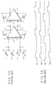
- a comparator circuit of the present invention includes a circuit constituted by first, second and third switch circuits 11, 12; 21, 22; 31, 32, 41, 42.
- the first switch circuits 11 and 12 are for connecting two differential input terminals 1 and 2 of a differential amplifier circuit 10 to inverting output terminals 3 and 4 thereof, respectively.
- the second switch circuits 21 and 22 are for connecting the two differential input terminals 1 and 2 of the differential amplifier circuit 10 to one end of at least capacitors C1 and C1', respectively.
- the third switch circuits 31, 32, 41 and 42 are for selectively connecting the other ends of the capacitors C1 and C1' to one of a plurality of input terminals.
- the two output terminals of the differential amplifier circuit 10 are connected to two input terminals of a differential amplifier circuit 20 through capacitors C2 and C2', respectively.
- the two differential input terminals of the differential amplifier circuit 20 are connected to switch circuits 51 and 52 for connecting the differential input terminals thereof to respective inverting output terminals.
- the open/close operations of the switch circuits 11, 12, 21, 22, 31, 32, 41 and 42 are controlled in accordance with the following order. That is,
- the order of the steps (4), (5) and (6) may be interchanged if the step (4) is executed earlier than the step (6). Further, the steps (4) and (5) may be simultaneously executed.
- Fig. 1B is a timing chart showing a method of controlling the comparator circuit in accordance with the embodiment of the present invention.
- Reference marks ⁇ s, ⁇ s1, ⁇ s2, ⁇ s3 and ⁇ c shown in Fig. 1B denote signals for controlling the switch circuits 11, 12, 21, 22, 31, 32, 41, 42, 51 and 52 shown in Fig. 1A.
- the respective switch circuit stands in an on-state when the control signal is at an "H” level whereas the switch circuit stands in an off-state when the control signal is at a "L" level.
- the switch circuits 31 and 32 are controlled by the control signal ⁇ s
- the switch circuits 11 and 12 are controlled by the control signal ⁇ s1
- the switch circuits 21 and 22 are controlled by the control signal ⁇ s2
- the switch circuits 51 and 52 are controlled by the control signal ⁇ s3
- the switch circuits 41 and 42 are controlled by the control signal ⁇ c .
- C1 and C1' are equal to each other and C2 and C2' are equal to each other.
- Phase 1 When ⁇ s, ⁇ s1, ⁇ s2 and ⁇ s3 are at the "H” level whereas ⁇ c is at the "L” level.
- One end of the capacitors C1 and C1' are supplied with the input signals V1 and V3 by the switch circuits 31 and 32.
- the differential amplifier circuits 10 and 20 have their input terminals and output terminals which are opposite in phase and connected to each other by the switch circuits 11 and 12 and the switch circuits 51 and 52.
- the input terminal 1 is connected to the output terminal 3 whereas the input terminal 2 is connected to the output terminal 4.
- V11 - V12 ⁇ 2A/(1 + 2A) ⁇ x V OF ⁇ V OF
- Phase 2 When ⁇ s2 becomes "L" earlier than ⁇ s, ⁇ s1 and ⁇ s3 , the switch circuits 21 and 22 are opened whereby the capacitors C1 and C1' are disconnected from the input terminals 1 and 2 of the differential amplifier circuit 1. At this time, sampling of the input voltages V1 and V3 are completed.
- the clock field through-noises are inputted to C1 and C1' by changing the state of ⁇ s2 to "L".
- the difference between both ends of the respective switch circuits 21 and 22 immediately before ⁇ s2 becomes “L” can be represented by expression (1).
- the voltage difference between the input terminals 1 and 2 of the differential amplifier circuit 10 is very slight in comparison with the amplitude of ⁇ s2 .
- the clock field through-noises inputted into C1 and C1' are in phase and of the same level.
- Phase 3 Subsequently to the change on ⁇ s2 , when ⁇ s becomes "L", the switch circuits 31 and 32 are opened so that C1 and C1' are cut off from V1 and V3. Even in this case, the clock field through-noises are inputted to C1 and C1'. However, since the other terminals 5 and 6 of C1 and C1' have been already disconnected from the input terminals of the differential amplifier circuit 10 by the switch circuits 21 and 22, the floating capacitances in the terminals 5 and 6 are sufficiently smaller than C1 and C1'. As a result, the influence of the clock field through-noises from ⁇ s on the charge stored in C1 and C1' can be ignored.
- Phase 4 Subsequently, when ⁇ s1 becomes “L” and ⁇ c becomes "H", the switch circuits 11 and 12, which have allowed the input and output terminals of the differential amplifier circuit 10, which are opposite in phase, to be short-circuited, are opened, and the switch circuits 41 and 42 are closed so that one terminal of C1 and C1' is applied with the input signal V2 and V4, respectively.
- the clock field through-noises from the switch circuits 11 and 12 are inputted to the input terminals 1 and 2 of the differential amplifier circuit 1. However, even in this case, the voltage difference between the input terminals 1 and 2 are very slight in comparison with the amplitude of ⁇ s1 as represented by expression (1).
- the clock field through-noises are in phase and of the same level, and therefore removed due to the in-phase removing characteristics of the differential amplifier circuit 10.
- Phase 5 When ⁇ s2 becomes “H” and ⁇ s3 becomes “L”, the switch circuits 21 and 22 are closed and the switch circuits 51 and 52 are opened. The input terminals 1 and 2 of the differential amplifier circuit 10 are again connected to the other terminals of C1 and C1' by closing the switch circuits 21 and 22. Since, in phase 4, the differential amplifier circuit 10 is in the operating state and the differential amplifier circuit 20 is also in the operating state with the switch circuits 51 and 52 opened, the comparison operation of the input voltage as the comparator circuit is started from this time. The input voltage V1 and V3 are stored in C1 and C1' in phase 1, and V2 and V4 are inputted thereto in phase 4.
- V11' - V12' V2 - V1 - (V4 - V3)
- V out A (V1 - V2 - V3 + V4)
- V out is operative as the comparator circuit.
- the timing of changing the state of ⁇ s3 to "L” to open the switch circuits 51 and 52 is preferably later than the timing of changing the state of ⁇ s2 to "L” to open the switch circuits 11 and 12.
- the switch circuits 21 and 22 are inserted between the differential amplifier circuit 10 and the capacitors C1 and C1' in the circuit of the invention shown in Fig. 1A, and the open/close operations of the respective switch circuits are controlled in accordance with the timing chart shown in Fig. 1B.
- the clock field through-noises from the input switch circuits 31 and 32 which result in the problem in the conventional comparator circuit, are not inputted to the differential amplifiers.
- the conventional comparator circuit although the influence of the clock field through-noises on the comparison operation is reduced, they are inputted to the differential amplifier circuit which is in the operating state. As a result, the clock field through-noises are amplified to be outputted.
- the comparison time of the comparator circuit is thus excessively required.
- the clock field through-noises are large, the output signal of the differential amplifier circuit is saturated so that the comparison operation per se may not be performed.
- the clock field through-noises from the input switch circuits 31 and 32 are not inputted to the differential amplifier circuit because the switch circuits 21 and 22 are opened. Also the differential amplifier circuit can remain balanced so that the input and output terminals thereof are short-circuited immediately until the comparison operation starts in phase 5. For that reason, even when the same differential amplifier circuit is used, it can be operated with the shortest comparison time.
- the clock field through-noises from the switch circuits are obviated.
- the noises inputted to C1 and C1' do not adversely affect the differential amplifier circuit due to the in-phase removing characteristics of the differential amplifier circuit because they are in phase and at the same level.
- switch circuits 21 and 22 are inserted between C11, C12, C21, C22 and input terminals 1, 2 of the differential amplifier circuit 10, respectively.
- the number of switch circuits is slightly increased in comparison with the conventional circuit, and therefore the increase in the entire layout area is confined to a minimum.
- switch circuits are added to two input terminals of the differential amplifier circuit. Also the respective switch circuits are controlled so that the clock field through-noises inputted from the input switch circuits are not inputted to the differential amplifier circuit. As a result, a high-speed comparator can be realised.
Landscapes
- Physics & Mathematics (AREA)
- Nonlinear Science (AREA)
- Manipulation Of Pulses (AREA)
- Measurement Of Current Or Voltage (AREA)
- Analogue/Digital Conversion (AREA)
Applications Claiming Priority (2)
| Application Number | Priority Date | Filing Date | Title |
|---|---|---|---|
| JP190574/93 | 1993-07-30 | ||
| JP19057493A JP3222276B2 (ja) | 1993-07-30 | 1993-07-30 | コンパレータ回路およびコンパレータ回路の制御方法 |
Publications (1)
| Publication Number | Publication Date |
|---|---|
| EP0637135A1 true EP0637135A1 (de) | 1995-02-01 |
Family
ID=16260330
Family Applications (1)
| Application Number | Title | Priority Date | Filing Date |
|---|---|---|---|
| EP94305645A Withdrawn EP0637135A1 (de) | 1993-07-30 | 1994-07-29 | Komparator-Schaltung und Verfahren zur Steuerung des Komparator-Schaltkreises |
Country Status (4)
| Country | Link |
|---|---|
| US (1) | US5565800A (de) |
| EP (1) | EP0637135A1 (de) |
| JP (1) | JP3222276B2 (de) |
| TW (1) | TW256968B (de) |
Cited By (4)
| Publication number | Priority date | Publication date | Assignee | Title |
|---|---|---|---|---|
| EP0729223A2 (de) * | 1995-02-21 | 1996-08-28 | Plessey Semiconductors Limited | Offsetspannungskompensationsschaltung |
| EP0691741A3 (de) * | 1994-07-05 | 1998-05-20 | Matsushita Electric Industrial Co., Ltd. | Verriegelungsschaltung |
| WO1999013584A1 (en) * | 1997-09-05 | 1999-03-18 | Cirrus Logic, Inc. | Method and system for sliced integration within flash analog to digital converters in read channel circuits |
| US5990814A (en) * | 1997-09-05 | 1999-11-23 | Cirrus Logic, Inc. | Method and circuit for calibration of flash analog to digital converters |
Families Citing this family (13)
| Publication number | Priority date | Publication date | Assignee | Title |
|---|---|---|---|---|
| JP2865026B2 (ja) * | 1995-06-30 | 1999-03-08 | 日本電気株式会社 | 比較器 |
| JPH10256884A (ja) * | 1997-03-12 | 1998-09-25 | Mitsubishi Electric Corp | 電圧比較器及びa/dコンバータ |
| DE19713144C2 (de) * | 1997-03-27 | 1999-01-28 | Siemens Ag | Komparator für großen Versorgungsspannungsbereich |
| JP2000114939A (ja) | 1998-10-05 | 2000-04-21 | Nec Corp | クロック信号生成装置 |
| US6359475B1 (en) * | 2000-08-30 | 2002-03-19 | Microchip Technology Incorporated | High-speed, low-power sample and hold circuit |
| JP3616353B2 (ja) * | 2001-06-14 | 2005-02-02 | Necマイクロシステム株式会社 | 電圧比較回路 |
| KR20080068011A (ko) | 2005-11-21 | 2008-07-22 | 마츠시타 덴끼 산교 가부시키가이샤 | 완전 차동형 비교기 및 완전 차동형 증폭회로 |
| US7336214B2 (en) * | 2005-12-16 | 2008-02-26 | Alexander Krymski | Analog to digital converter circuit with offset reduction and image sensor using the same |
| JP4961159B2 (ja) * | 2006-04-14 | 2012-06-27 | オリンパス株式会社 | 増幅回路及びその応用回路 |
| JP4545116B2 (ja) * | 2006-06-12 | 2010-09-15 | ルネサスエレクトロニクス株式会社 | 電圧比較回路 |
| US7541852B2 (en) * | 2006-12-28 | 2009-06-02 | Intel Corporation | Self-correcting buffer |
| JP5439590B2 (ja) * | 2010-04-06 | 2014-03-12 | 株式会社半導体理工学研究センター | 比較器、差動アンプ回路、及びアナログデジタル変換器 |
| US11169218B2 (en) | 2018-12-21 | 2021-11-09 | Analog Devices, Inc. | Current monitor with fault detection |
Citations (15)
| Publication number | Priority date | Publication date | Assignee | Title |
|---|---|---|---|---|
| US4237390A (en) * | 1978-09-28 | 1980-12-02 | National Semiconductor Corporation | Switching comparator |
| WO1983003932A1 (en) * | 1982-04-23 | 1983-11-10 | Motorola, Inc. | A switched capacitor comparator |
| EP0101571A1 (de) * | 1982-07-30 | 1984-02-29 | Kabushiki Kaisha Toshiba | Spannungsdifferenz-Verstärker |
| FR2536922A1 (fr) * | 1982-11-26 | 1984-06-01 | Efcis | Comparateur logique a plusieurs fonctions |
| EP0145100A2 (de) * | 1983-12-07 | 1985-06-19 | American Microsystems, Incorporated | Offsetverminderung für schnelle Komparatoren mit in Serie geschalteten Eintaktverstärkerstufen |
| EP0150606A1 (de) * | 1983-12-28 | 1985-08-07 | Fujitsu Limited | Komparator-Schaltungsanordnung |
| US4547683A (en) * | 1982-10-18 | 1985-10-15 | Intersil, Inc. | High speed charge balancing comparator |
| US4560890A (en) * | 1982-08-31 | 1985-12-24 | Tokyo Shibaura Denki Kabushiki Kaisha | Autozeroed comparator |
| US4900952A (en) * | 1988-10-07 | 1990-02-13 | Mitsubishi Denki Kabushiki Kaisha | Voltage comparison apparatus |
| GB2222330A (en) * | 1988-08-05 | 1990-02-28 | Gen Electric Co Plc | Delta sigma modulator |
| US5012244A (en) * | 1989-10-27 | 1991-04-30 | Crystal Semiconductor Corporation | Delta-sigma modulator with oscillation detect and reset circuit |
| US5028815A (en) * | 1989-01-16 | 1991-07-02 | U. S. Philips Corporation | Clocked comparator with offset reduction |
| EP0465249A1 (de) * | 1990-07-05 | 1992-01-08 | Nippon Motorola Ltd. | Spannungsvergleichsschaltung mit Abtast-Halte-Schaltungsanordnung |
| US5113090A (en) * | 1989-08-30 | 1992-05-12 | Hitachi Ltd. | Voltage comparator |
| EP0488893A1 (de) * | 1990-11-30 | 1992-06-03 | Bull S.A. | Verfahren und Vorrichtung zur Übertragung binärer Differenzsignale und Verwendung in Carry-Select-Addierern |
Family Cites Families (6)
| Publication number | Priority date | Publication date | Assignee | Title |
|---|---|---|---|---|
| JPS58170213A (ja) * | 1982-03-31 | 1983-10-06 | Toshiba Corp | 電圧比較回路 |
| JPS6276099A (ja) * | 1985-09-30 | 1987-04-08 | Toshiba Corp | サンプル・アンド・ホ−ルド回路 |
| US4633222A (en) * | 1985-10-01 | 1986-12-30 | Rca Corporation | Clock shaping circuit and method |
| JP2698225B2 (ja) * | 1991-04-15 | 1998-01-19 | シャープ株式会社 | サンプルホールド回路 |
| US5258664A (en) * | 1991-07-05 | 1993-11-02 | Silicon Systems, Inc. | Operational amplifier with self contained sample and hold and auto zero |
| US5341050A (en) * | 1992-03-20 | 1994-08-23 | Hughes Aircraft Company | Switched capacitor amplifier circuit operating without serially coupled amplifiers |
-
1993
- 1993-07-30 JP JP19057493A patent/JP3222276B2/ja not_active Expired - Lifetime
-
1994
- 1994-07-20 TW TW083106645A patent/TW256968B/zh not_active IP Right Cessation
- 1994-07-28 US US08/282,032 patent/US5565800A/en not_active Expired - Lifetime
- 1994-07-29 EP EP94305645A patent/EP0637135A1/de not_active Withdrawn
Patent Citations (15)
| Publication number | Priority date | Publication date | Assignee | Title |
|---|---|---|---|---|
| US4237390A (en) * | 1978-09-28 | 1980-12-02 | National Semiconductor Corporation | Switching comparator |
| WO1983003932A1 (en) * | 1982-04-23 | 1983-11-10 | Motorola, Inc. | A switched capacitor comparator |
| EP0101571A1 (de) * | 1982-07-30 | 1984-02-29 | Kabushiki Kaisha Toshiba | Spannungsdifferenz-Verstärker |
| US4560890A (en) * | 1982-08-31 | 1985-12-24 | Tokyo Shibaura Denki Kabushiki Kaisha | Autozeroed comparator |
| US4547683A (en) * | 1982-10-18 | 1985-10-15 | Intersil, Inc. | High speed charge balancing comparator |
| FR2536922A1 (fr) * | 1982-11-26 | 1984-06-01 | Efcis | Comparateur logique a plusieurs fonctions |
| EP0145100A2 (de) * | 1983-12-07 | 1985-06-19 | American Microsystems, Incorporated | Offsetverminderung für schnelle Komparatoren mit in Serie geschalteten Eintaktverstärkerstufen |
| EP0150606A1 (de) * | 1983-12-28 | 1985-08-07 | Fujitsu Limited | Komparator-Schaltungsanordnung |
| GB2222330A (en) * | 1988-08-05 | 1990-02-28 | Gen Electric Co Plc | Delta sigma modulator |
| US4900952A (en) * | 1988-10-07 | 1990-02-13 | Mitsubishi Denki Kabushiki Kaisha | Voltage comparison apparatus |
| US5028815A (en) * | 1989-01-16 | 1991-07-02 | U. S. Philips Corporation | Clocked comparator with offset reduction |
| US5113090A (en) * | 1989-08-30 | 1992-05-12 | Hitachi Ltd. | Voltage comparator |
| US5012244A (en) * | 1989-10-27 | 1991-04-30 | Crystal Semiconductor Corporation | Delta-sigma modulator with oscillation detect and reset circuit |
| EP0465249A1 (de) * | 1990-07-05 | 1992-01-08 | Nippon Motorola Ltd. | Spannungsvergleichsschaltung mit Abtast-Halte-Schaltungsanordnung |
| EP0488893A1 (de) * | 1990-11-30 | 1992-06-03 | Bull S.A. | Verfahren und Vorrichtung zur Übertragung binärer Differenzsignale und Verwendung in Carry-Select-Addierern |
Cited By (5)
| Publication number | Priority date | Publication date | Assignee | Title |
|---|---|---|---|---|
| EP0691741A3 (de) * | 1994-07-05 | 1998-05-20 | Matsushita Electric Industrial Co., Ltd. | Verriegelungsschaltung |
| EP0729223A2 (de) * | 1995-02-21 | 1996-08-28 | Plessey Semiconductors Limited | Offsetspannungskompensationsschaltung |
| EP0729223A3 (de) * | 1995-02-21 | 1998-09-16 | Plessey Semiconductors Limited | Offsetspannungskompensationsschaltung |
| WO1999013584A1 (en) * | 1997-09-05 | 1999-03-18 | Cirrus Logic, Inc. | Method and system for sliced integration within flash analog to digital converters in read channel circuits |
| US5990814A (en) * | 1997-09-05 | 1999-11-23 | Cirrus Logic, Inc. | Method and circuit for calibration of flash analog to digital converters |
Also Published As
| Publication number | Publication date |
|---|---|
| JPH0743397A (ja) | 1995-02-14 |
| TW256968B (de) | 1995-09-11 |
| JP3222276B2 (ja) | 2001-10-22 |
| US5565800A (en) | 1996-10-15 |
Similar Documents
| Publication | Publication Date | Title |
|---|---|---|
| EP0637135A1 (de) | Komparator-Schaltung und Verfahren zur Steuerung des Komparator-Schaltkreises | |
| US5113090A (en) | Voltage comparator | |
| EP0709794B1 (de) | Halbleiterschaltung und ihre Anwendung in einer Operationsschaltung, einem Signalwandler und einem Signalverarbeitungssystem | |
| EP0582862B1 (de) | Verstärkerschaltung mit geschalteten Kapazitäten | |
| EP0508360B1 (de) | Abgetastete Bandabstandreferenzspannungsschaltung | |
| JP2708007B2 (ja) | サンプル・ホールド回路 | |
| EP0800271A2 (de) | Signalangepasster Filter | |
| EP0849883B1 (de) | Analog-Digital-Wandler | |
| US7030791B2 (en) | A/D conversion device having input level shift and output correction function | |
| US6437720B1 (en) | Code independent charge transfer scheme for switched-capacitor digital-to-analog converter | |
| US4110745A (en) | Analog to digital converter | |
| US4707624A (en) | Offset cancellation scheme for a differential reset stabilized latch | |
| US6046612A (en) | Self-resetting comparator circuit and method | |
| JPH0927883A (ja) | 画像読取信号処理装置 | |
| JP2916505B2 (ja) | 比較回路 | |
| JPH0313677B2 (de) | ||
| GB2209895A (en) | Storing sampled analogue electrical currents | |
| JPH0332109A (ja) | 比較器回路 | |
| US4531106A (en) | Switched capacitor circuits | |
| US7002507B2 (en) | Pipelined and cyclic analog-to-digital converters | |
| US4746871A (en) | Differential switched capacitor integrator using a single integration capacitor | |
| US6421341B1 (en) | High speed packet switching controller for telephone switching system | |
| US6097248A (en) | Switched capacitor amplifier with one-clock delay | |
| US20040113829A1 (en) | Analog to digital conversion circuit | |
| US6118333A (en) | Clock buffer circuit and clock signal buffering method which can suppress current consumption |
Legal Events
| Date | Code | Title | Description |
|---|---|---|---|
| PUAI | Public reference made under article 153(3) epc to a published international application that has entered the european phase |
Free format text: ORIGINAL CODE: 0009012 |
|
| AK | Designated contracting states |
Kind code of ref document: A1 Designated state(s): DE FR GB |
|
| STAA | Information on the status of an ep patent application or granted ep patent |
Free format text: STATUS: THE APPLICATION IS DEEMED TO BE WITHDRAWN |
|
| 18D | Application deemed to be withdrawn |
Effective date: 19950802 |