EP0637035B1 - Schaltungsstruktur für Speichermatrix und entsprechende Herstellungsverfahren - Google Patents
Schaltungsstruktur für Speichermatrix und entsprechende Herstellungsverfahren Download PDFInfo
- Publication number
- EP0637035B1 EP0637035B1 EP93830339A EP93830339A EP0637035B1 EP 0637035 B1 EP0637035 B1 EP 0637035B1 EP 93830339 A EP93830339 A EP 93830339A EP 93830339 A EP93830339 A EP 93830339A EP 0637035 B1 EP0637035 B1 EP 0637035B1
- Authority
- EP
- European Patent Office
- Prior art keywords
- source
- cells
- byte
- line
- transistors
- Prior art date
- Legal status (The legal status is an assumption and is not a legal conclusion. Google has not performed a legal analysis and makes no representation as to the accuracy of the status listed.)
- Expired - Lifetime
Links
Images


Classifications
-
- H—ELECTRICITY
- H10—SEMICONDUCTOR DEVICES; ELECTRIC SOLID-STATE DEVICES NOT OTHERWISE PROVIDED FOR
- H10B—ELECTRONIC MEMORY DEVICES
- H10B41/00—Electrically erasable-and-programmable ROM [EEPROM] devices comprising floating gates
- H10B41/40—Electrically erasable-and-programmable ROM [EEPROM] devices comprising floating gates characterised by the peripheral circuit region
-
- G—PHYSICS
- G11—INFORMATION STORAGE
- G11C—STATIC STORES
- G11C16/00—Erasable programmable read-only memories
- G11C16/02—Erasable programmable read-only memories electrically programmable
- G11C16/04—Erasable programmable read-only memories electrically programmable using variable threshold transistors, e.g. FAMOS
- G11C16/0408—Erasable programmable read-only memories electrically programmable using variable threshold transistors, e.g. FAMOS comprising cells containing floating gate transistors
- G11C16/0433—Erasable programmable read-only memories electrically programmable using variable threshold transistors, e.g. FAMOS comprising cells containing floating gate transistors comprising cells containing a single floating gate transistor and one or more separate select transistors
-
- H—ELECTRICITY
- H10—SEMICONDUCTOR DEVICES; ELECTRIC SOLID-STATE DEVICES NOT OTHERWISE PROVIDED FOR
- H10B—ELECTRONIC MEMORY DEVICES
- H10B41/00—Electrically erasable-and-programmable ROM [EEPROM] devices comprising floating gates
- H10B41/40—Electrically erasable-and-programmable ROM [EEPROM] devices comprising floating gates characterised by the peripheral circuit region
- H10B41/42—Simultaneous manufacture of periphery and memory cells
- H10B41/43—Simultaneous manufacture of periphery and memory cells comprising only one type of peripheral transistor
- H10B41/47—Simultaneous manufacture of periphery and memory cells comprising only one type of peripheral transistor with a floating-gate layer also being used as part of the peripheral transistor
-
- H—ELECTRICITY
- H10—SEMICONDUCTOR DEVICES; ELECTRIC SOLID-STATE DEVICES NOT OTHERWISE PROVIDED FOR
- H10B—ELECTRONIC MEMORY DEVICES
- H10B69/00—Erasable-and-programmable ROM [EPROM] devices not provided for in groups H10B41/00 - H10B63/00, e.g. ultraviolet erasable-and-programmable ROM [UVEPROM] devices
Definitions
- This invention relates to a circuit structure for a memory cells matrix.
- the invention relates to a matrix of EEPROM memory cells being of a type which comprises a cells matrix composed of plural rows and columns, each provided with a word line and a bit line respectively, wherein the bit lines are gathered into groups or bytes of adjacent lines which are simultaneously addressable, each of said cells incorporating a floating gate transistor connected serially to a selection transistor and having an additional control gate overlaying the floating gate.
- EEPROM memory structures while being non-volatile types, allow the information contained therein to be modified electrically at both the write and the erase phases of their operation. Furthermore, they distinguish themselves by the kind of their electric programming, which may take place in either the "page" mode or the "byte” mode.
- the state of any cell in the EEPROM memory can be altered by means of an electrons flow passing by tunnel effect through a thin layer of silicon oxide associated with the floating gate of the cell.
- the thin oxide region occupies a smaller area than the floating gate, whereat the electric charge is stored.
- the byte mode programming is carried out by splitting the control gate into segments which are common to a single byte (e.g., eight or sixteen bits).
- the control gate is then selected by means of a column decoder external of the cells matrix, and is enabled by a select transistor shared by all the cells in one row.
- the underlying technical problem of this invention is to provide a circuit structure for a matrix of memory cells, in particular of the EEPROM type, which has such structural and functional features as to improve the memory reliability, and extend its service life, while attenuating the deterioration of the tunnel oxide and obviating the programming problems when using negative voltages.
- a further object of the invention is to provide very high density integrated storage circuits which can occupy, for a given technology, a smaller circuit area than comparable circuits of conventional design. This would enable the manufacturing costs of high density storage circuits to be cut down drastically.
- a further object of the invention is to provide a circuit of a matrix of EEPROM memory cells wherein erasing of non addressed memory cells is avoided.
- EP-A-0 182 198 employs memory cells without selection transistors.
- the sources of the memory transistors of a byte (cf fig.5d) are connected to a common source area which is structurally independent for each byte and connected via enable transistors (129) to a source addressing line (126).
- the drains of all bytes are floating, the gates of the addressed byte (BYTE 1) are set to ground, and the source area of said addressed byte is set to Vpp.
- Vpp is supplied by said source addressing line (126) via an enable transistor which is switched on by Vpp applied to the word line WL2 controlling the non addressed adjacent byte (BYTE 2) in column direction.
- BYTE 3 BYTE 4
- BYTE 4 further non addressed bytes
- the intermediate voltage (5V) decreases the voltage difference between the gates and the sources and thus avoids erasing of said further non addressed bytes.
- the solutive idea on which this invention stands is one of splitting the so-called source line into regular segments shared by the cells of a single byte (having eight or sixteen bits, for example) and decoding such segments when a desired byte is programmed.
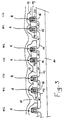
- the structure 1 is constructed in the form of a semiconductor integrated circuit incorporating thousands of cells 2. Shown diagramatically in Figure 1 is, however, just a portion of this circuit.
- the matrix provided by the structure 1 comprises a plurality of rows 3 and plurality of columns 4.
- Each row 3 includes a so-called word line WL and a corresponding control gate line CG.
- the columns 4 include the so-called bit lines of the matrix.
- bit lines BL are gathered into bytes 9, that is into groups of eight BL 0 ,...,BL 7 or sixteen adjacent lines which can be addressed simultaneously.
- bit line BL interconnects all the drain terminals of the common selection transistors 5 on a given column 4 of the matrix.
- Each selection transistor 5 is associated with and connected serially to a floating gate EEPROM cell 2.
- the cell 2 is of the type with a double level of polysilicon, and has a basic structure substantially of the FLOTOX type.
- the core of the memory cell 2 comprises a MOS transistor having a floating gate 12 where the electric charge is stored identifyings the two different, "written” or “erased", states of the cell.
- the floating gate is shown in Figure 2.
- the cell 2 would include a second, or control, gate 8, which is coupled capacitively to the floating gate 12 through an intervening dielectric layer called "interpoly". A voltage is transferred through said dielectric layer to the floating gate 12 from the control gate 8 during the write and/or erase phases of the cell 2.
- the control terminal of the control gate 8 is shared by all the cells 2 which form any one row 3 in the structure 1.
- Each row 3 of the matrix 1 is provided, to that aim, with a dedicated connection line CG interconnecting the gates 8.
- the structure 1 further comprises plural source addressing columns 7, each associated with a corresponding byte 9.
- Such columns 7 are also referred to as source addressing lines SL.
- the lines SL are each connected between each pair of adjacent bytes 9, that is to say, a column 7 is provided for each group of bit lines BL forming a byte 9.
- Each source addressing line SL connects the source terminals of a series of enable transistors A and B aligned on one column.
- the transistors denoted by A are provided at the crossover of each word line WL with the column 7, whereas the transistors denoted by B are provided at the crossover of each connection line CG connecting the control gates 8 to the column 7.
- the source terminals of all the transistors incorporated to the cells 2 of a single byte 9 are led to one and the same corresponding source line SL.
- the enable transistors A and B present in the source addressing line SL are not strictly necessary, although their provision has the advantage of minimizing noise, as explained hereinafter.
- the transistors A are intended for selecting the segment of that source line SL in the row 3 which would be addressed when accessing the memory structure. Each transistor A is driven from its respective word line WL.
- the transistors B are basically additional enable transistors. They are driven from their respective connection line CG and should be a high-voltage type in order to withstand the voltages that are applied during the erase phase.
- Each transistor B only represents a small increase in the series resistance of its respective source line SL. This resistance may be minimized, if desired, by appropriate selection of the transistor B length and width, or even removed altogether by shorting the transistors with an implant or a connecting bridge of polysilicon or metal.
- positive voltage pulses are usually employed for writing and erasing a given cell, which pulses are applied to the cell terminals such that a sufficient electric field is generated to induce a flow of current through the tunnel oxide layer.
- the memory structure of this invention provides for the use of a negative voltage, to be applied to the control gate 8 of each predetermined cell 2 during the write phase.
- the voltage at the control gate 8 is decoded by rows, as is that applied to the gate of the selection transistor 5.
- the voltage at the drain terminal is on the contrary decoded by columns, as is that at the source terminals of the line SL.
- the erase and read phases for the selected byte are run in a similar manner, with the difference that no negative voltages are applied here to the various terminals.
- the voltage on the word line during the erase phase may be zero.
- Table II shows the voltage values being applied to a byte which has not been selected but is present in the same row as the selected byte.
- Table III shows the voltage levels being applied to a byte which has not been selected but is present in the same column as the selected byte.
- V SOURCE [V] V DRAIN [V] WL select tr. [V] V CG [V] WRITE float 5 6 -8 ERASE 0 float 6 16 READ 0 1 5 3
- the polarizations applied to the various terminals are transferred in the same way as previously described; that is to say, the control gate decoding is carried out by rows, whereas the decoding of the drain and the source terminals is carried out by columns.
- the write phase is characterized by the use of a negative voltage at the control gate 8 and a positive voltage at the drain terminal of the cell 2; this allows generation of a sufficiently strong electric field to draw electrons from the floating gate 12.
- this operation does impose some noise on all the cells in one row 3.
- the negative voltage would also be applied to their control gate 8, which is in common with the line CG for all the cells in the same row 3.
- This noise may be difficult to suppress in the byte programming mode; but the effect of the noise can be minimized by appropriate adjustment of the values of the applied voltages.
- both the transistor A and the transistor B are conducting, and each cell 2 of the selected byte 9 is injected by electrons at the floating gate 12 through the channel region.
- the source lines SL of the unselected columns 7 are brought to a voltage of 5 Volts.
- the voltage is transferred to all the source segments related to each byte because the transistors A and B are conducting.
- the read phase is run in quite a conventional manner.
- the cells 2 in the matrix 1 are implemented in the MOS technology, starting with a P-doped semiconductor substrate 10, which has been formed with either N-type or P-type wells.
- the description to follow will begin with the step of photolithographically defining active area regions on the substrate 10.
- the common source regions 6 of cells 2 in the same byte 9 are structurally and electrically separate from those of the adjacent bytes, as brought out by Figure 5.
- field oxide 22 allows such regions 6 to be demarcated.
- the gate oxide is formed to different depths according to the different transistor types. For instance, a tunnel oxide 24 thickness of about 9 nm is preferred for the floating gate cells 2, while a thickness of about 20 nm would be appropriate for the selection transistors 5.
- the former may have a gate oxide 26 formed to either a thickness of 20 nm or 30 nm, that is, for a low or a high voltage, whilst the latter transistor B is to expressedly withstand high voltages and requires a thickness of about 30 nm for the gate oxide 16.
- steps such as by growing a first oxide layer of about 24 nm onto the surface of the substrate 10.
- This first layer would be masked with a resist and etched in those areas where the low-voltage oxide is to be grown. The resist is then removed, and a second oxide layer of about 18 nm grown.
- the depth of the first layer would also be increased.
- a subsequent masking step with a resist will enable the high- and low-voltage oxide 16, 26 areas to be protected, and the oxide layer etched away in the tunnel areas. Removal of the resist and subsequent growth of the tunnel dielectric 24 bring to completion the thickness of the low- and high-voltage oxides 16 and 26 as well.
- the process continues with the deposition, doping, and photolithographic definition of the first polycrystalline silicon (polysilicon) layer 20 for the floating gates 12 of the cells 2.
- a so-called interpoly dielectric layer 25 is formed over the first polysilicon layer 20.
- This interpoly layer 15 is removed, however, along the source addressing line SL shown in Figure 3 to later obtain standard transistors A and B having no floating gates.
- the other areas of the matrix 1 are protected with a photoresist during this operation.
- a second polysilicon layer 21 will allow the formation of the control gates 8 and those of the selection transistors 5, as well as the gates of the enable transistors A and B.
- the source and drain implantations are carried out for the cells 2, the selection transistors 5, and the active areas 15 of the transistors A and B, using at least one species of the N type.
- circuit structure of this invention as obtained with the process described hereinabove, does solve the technical problem and afford a number of advantages as follows.
- this solution allows the programming to be handled for each individual byte even where negative voltages are used during the write phase.
- the use of a negative voltage at the control gate 8 allows the voltage applied to the drain terminal to be lowered while maintaining, across the thin oxide, an electric field which is the equal of that provided in conventional cells. Thus, the deterioration of the thin tunnel oxide can be greatly reduced.
- the use of a negative voltage at the control gate 8 of the cells 2 during the write phase allows the voltage requirement across the tunnel oxide for obtaining a desired programming current to be distributed.
- the circuit of this invention can be integrated within a smaller area than a conventional cell of equal technology. Since the inventive cell works on the basis of a Fowler-Nordheim tunnel effect, and its intrinsic threshold may be selected close to zero, this structure would suit in particular low-voltage supply applications.
Landscapes
- Engineering & Computer Science (AREA)
- Microelectronics & Electronic Packaging (AREA)
- Manufacturing & Machinery (AREA)
- Non-Volatile Memory (AREA)
- Semiconductor Memories (AREA)
Claims (12)
- Matrixschaltung aus EEPROM-Speicherzellen des Typs, der eine Matrix von Zellen (2) enthält, welche mehrere Reihen (3) und Spalten (4) beinhaltet, von denen jede Reihe (3) mit einer Wortleitung (WL) und einer Steuergateleitung (CG) ausgestattet ist und jede Spalte (4) eine Bitleitung (BL) aufweist, wobei die Bitleitungen (BL) zu Gruppen von gleichzeitig adressierbaren benachbarten Leitungen zusammengefaßt sind, um dadurch die Matrixzellen zu Bytes (9) zu gruppieren, und die Matrixzellen (2) jeweils einen Transistor mit schwimmendem Gate beinhalten, der an ein mit der Steuergateleitung (CG) verbundenes Steuergate (8) gekoppelt und mit dem Drain seriell an einen Auswahltransistor (5) angeschlossen ist,
dadurch gekennzeichnet, daß
die Zellen (2) jedes einzelnen Bytes (9) eine gemeinsame Sourcefläche (6) besitzen, wobei diese Fläche baulich unabhängig für jedes Byte (9) ist und zu einer zugehörigen Source-Adressierleitung (SL) geführt ist, die sich entlang einer Matrixspalte (7) erstreckt, um das Löschen von nicht-adressierten Bytes zu vermeiden, indem an die Sourcefläche eine Spannung angelegt wird, welche die Spannungsdifferenz zwischen dem Steuergate und der Sourcefläche der nicht-adressierten Bytes verringert. - Schaltung nach Anspruch 1, dadurch gekennzeichnet, daß die Source-Adressierleitung (SL) im wesentlichen aufgespalten ist in Segmente, die von den Zellen (2) jedes einzelnen Bytes (9) gemeinsam benutzt werden.
- Schaltung nach Anspruch 1, dadurch gekennzeichnet, daß die Source-Adressierleitung decodiert wird, wenn ein gewünschtes Byte (9) ausgewählt wird.
- Schaltung nach Anspruch 2, dadurch gekennzeichnet, daß jedes Segment (6) individuell adressierbar ist und decodiert wird, wenn auf das gewünschte Byte (9) zugegriffen oder dieses programmiert wird.
- Schaltung nach Anspruch 1, dadurch gekennzeichnet, daß die Source-Adressierleitung (SL) mindestens einen Freigabetransistor (A) aufweist, der an die Sourcezonen (6) der Zellen (2) ein und desselben Bytes (9) angeschlossen ist.
- Schaltung nach Anspruch 5, dadurch gekennzeichnet, daß der Freigabetransistor (A) an der Kreuzungsstelle jeder Wortleitung (WL) mit der Sourceleitung (SL) vorgesehen ist.
- Schaltung nach Anspruch 1, dadurch gekennzeichnet, daß die Source-Adressierleitung (SL) mindestens ein Paar Freigabetransistoren (A, B) aufweist, die an die Sourcezone (6) ein und desselben Bytes (9) angeschlossen sind.
- Schaltung nach Anspruch 7, dadurch gekennzeichnet, daß der erstere (A) von den Freigabetransistoren (A, B) an der Kreuzungsstelle jeder Wortleitung (WL) mit der Source-Adressierleitung (SL) vorgesehen ist.
- Schaltung nach Anspruch 7, dadurch gekennzeichnet, daß letzterer von den Freigabetransistoren an der Kreuzungsstelle jeder Steuergateleitung (CG) der Steuergats (8) mit der Source-Adressierleitung (SL) vorgesehen ist.
- Verfahren, um in MOS-Technologie eine Matrix (1) aus Speicherzellen (2) des Typs herzustellen, bei dem in MOS-Technologie auf einem Halbleitersubstrat (10) die Zellen (2) ausgebildet sind, die Transistoren mit schwimmendem Gate (12) sowie aktive Source- (6) und Drainbereiche enthalten und jeweils mit dem Drain in Serie zu einem jeweiligen Auswahltransistor (5) geschaltet sind, dadurch gekennzeichnet, daß es die Ausbildung mehrerer Adressierleitungen (SL) für die aktiven Sourceflächen (6) vorsieht, die Adressierleitungen sich entlang den Spalten (7) der Matrix (1) erstrecken und jeweils Freigabetransistoren (A, B) enthalten, die gleichzeitig mit den Transistoren mit schwimmendem Gate und den Auswahltransistoren (5) ausgebildet werden, daß es die Ausbildung einer strukturell unabhängigen und gemeinsamen Sourcefläche (6) für die Zellen (2) jedes einzelnen Bytes (9) vorsieht, und daß es vorsieht, jede gemeinsame Sourcefläche mit dem Freigabetransistor zu verbinden.
- Verfahren nach Anspruch 10, dadurch gekennzeichnet, daß die aktiven Sourceflächen (6) der in die Zellen (2) eines gegebenen Bytes (9) eingebauten Transistoren gemeinsam mit ein und derselben zugehörigen Source-Adressierleitung (SL) eingebaut werden.
- Schaltung nach Anspruch 1, dadurch gekennzeichnet, daß die Sourceanschlüsse der in die Zellen (2) eingebauten Transistoren eines vorbestimmten Bytes (9) an ein und dieselbe zugehörige Source-Adressierleitung (SL) angeschlossen sind.
Priority Applications (5)
| Application Number | Priority Date | Filing Date | Title |
|---|---|---|---|
| DE69305986T DE69305986T2 (de) | 1993-07-29 | 1993-07-29 | Schaltungsstruktur für Speichermatrix und entsprechende Herstellungsverfahren |
| EP93830339A EP0637035B1 (de) | 1993-07-29 | 1993-07-29 | Schaltungsstruktur für Speichermatrix und entsprechende Herstellungsverfahren |
| JP6197977A JPH07147390A (ja) | 1993-07-29 | 1994-07-29 | メモリセル・マトリクス用回路構造およびその製造方法 |
| US08/474,735 US5597750A (en) | 1993-07-29 | 1995-06-07 | Method of manufacturing a matrix of memory cells having control gates |
| US08/688,233 US5677871A (en) | 1993-07-29 | 1996-07-29 | Circuit structure for a memory matrix and corresponding manufacturing method |
Applications Claiming Priority (1)
| Application Number | Priority Date | Filing Date | Title |
|---|---|---|---|
| EP93830339A EP0637035B1 (de) | 1993-07-29 | 1993-07-29 | Schaltungsstruktur für Speichermatrix und entsprechende Herstellungsverfahren |
Publications (2)
| Publication Number | Publication Date |
|---|---|
| EP0637035A1 EP0637035A1 (de) | 1995-02-01 |
| EP0637035B1 true EP0637035B1 (de) | 1996-11-13 |
Family
ID=8215209
Family Applications (1)
| Application Number | Title | Priority Date | Filing Date |
|---|---|---|---|
| EP93830339A Expired - Lifetime EP0637035B1 (de) | 1993-07-29 | 1993-07-29 | Schaltungsstruktur für Speichermatrix und entsprechende Herstellungsverfahren |
Country Status (4)
| Country | Link |
|---|---|
| US (2) | US5597750A (de) |
| EP (1) | EP0637035B1 (de) |
| JP (1) | JPH07147390A (de) |
| DE (1) | DE69305986T2 (de) |
Cited By (1)
| Publication number | Priority date | Publication date | Assignee | Title |
|---|---|---|---|---|
| USRE41734E1 (en) | 1995-12-06 | 2010-09-21 | Infineon Technologies Ag | Read-only memory having specially output circuits and word line connected to a group of memory cells |
Families Citing this family (17)
| Publication number | Priority date | Publication date | Assignee | Title |
|---|---|---|---|---|
| KR100190522B1 (ko) * | 1995-06-09 | 1999-06-01 | 김영환 | 반도체 메모리 집적회로 및 그 제조방법 |
| FR2735896B1 (fr) * | 1995-06-21 | 1997-08-22 | Sgs Thomson Microelectronics | Memoire eeprom programmable et effacable par effet de fowler-nordheim |
| US6291851B1 (en) * | 1995-07-21 | 2001-09-18 | Rohm Co., Ltd. | Semiconductor device having oxide layers formed with different thicknesses |
| US5963478A (en) * | 1995-12-06 | 1999-10-05 | Siemens Aktiengesellschaft | EEPROM and method of driving the same |
| DE19545523C2 (de) * | 1995-12-06 | 2001-02-15 | Siemens Ag | EEPROM und Verfahren zur Ansteuerung desselben |
| DE69626631T2 (de) * | 1996-06-05 | 2003-11-06 | St Microelectronics Srl | Seitenmodusspeicher mit Mehrpegelspeicherzellen |
| JPH104149A (ja) * | 1996-06-14 | 1998-01-06 | Oki Electric Ind Co Ltd | 半導体記憶装置および製造方法 |
| US5861333A (en) * | 1996-10-25 | 1999-01-19 | United Microelectonics Corp. | Method of tunnel window process for EEPROM cell technology |
| US5763307A (en) * | 1996-11-08 | 1998-06-09 | Advanced Micro Devices, Inc. | Block select transistor and method of fabrication |
| USRE37419E1 (en) * | 1997-06-05 | 2001-10-23 | Aplus Flash Technology Inc. | Flash memory array and decoding architecture |
| US6071778A (en) * | 1998-02-20 | 2000-06-06 | Stmicroelectronics S.R.L. | Memory device with a memory cell array in triple well, and related manufacturing process |
| IT1301880B1 (it) | 1998-07-30 | 2000-07-07 | St Microelectronics Srl | Circuito elettronico di memoria e corrispondente metodo difabbricazione |
| JP2002016238A (ja) * | 2000-06-29 | 2002-01-18 | Mitsubishi Electric Corp | 半導体装置 |
| US7483505B2 (en) * | 2001-04-27 | 2009-01-27 | The Directv Group, Inc. | Unblind equalizer architecture for digital communication systems |
| US7388251B2 (en) * | 2004-08-11 | 2008-06-17 | Micron Technology, Inc. | Non-planar flash memory array with shielded floating gates on silicon mesas |
| EP1727152B1 (de) * | 2005-05-18 | 2008-12-24 | STMicroelectronics SA | EEPROM-Speicherarchitektur |
| US8320191B2 (en) | 2007-08-30 | 2012-11-27 | Infineon Technologies Ag | Memory cell arrangement, method for controlling a memory cell, memory array and electronic device |
Family Cites Families (16)
| Publication number | Priority date | Publication date | Assignee | Title |
|---|---|---|---|---|
| JPS5974677A (ja) * | 1982-10-22 | 1984-04-27 | Ricoh Co Ltd | 半導体装置及びその製造方法 |
| US4698787A (en) * | 1984-11-21 | 1987-10-06 | Exel Microelectronics, Inc. | Single transistor electrically programmable memory device and method |
| JPS6260266A (ja) * | 1985-09-10 | 1987-03-16 | Toshiba Corp | 不揮発性半導体記憶装置 |
| FR2622038B1 (fr) * | 1987-10-19 | 1990-01-19 | Thomson Semiconducteurs | Procede de programmation des cellules memoire d'une memoire et circuit pour la mise en oeuvre de ce procede |
| JPH01137496A (ja) * | 1987-11-20 | 1989-05-30 | Mitsubishi Electric Corp | 不揮発性半導体記憶装置 |
| US4888735A (en) * | 1987-12-30 | 1989-12-19 | Elite Semiconductor & Systems Int'l., Inc. | ROM cell and array configuration |
| FR2626401B1 (fr) * | 1988-01-26 | 1990-05-18 | Sgs Thomson Microelectronics | Memoire eeprom a grille flottante avec transistor de selection de ligne de source |
| US4999812A (en) * | 1988-11-23 | 1991-03-12 | National Semiconductor Corp. | Architecture for a flash erase EEPROM memory |
| US5081054A (en) * | 1989-04-03 | 1992-01-14 | Atmel Corporation | Fabrication process for programmable and erasable MOS memory device |
| KR930000869B1 (ko) * | 1989-11-30 | 1993-02-08 | 삼성전자 주식회사 | 페이지 소거 가능한 플래쉬형 이이피롬 장치 |
| US5188976A (en) * | 1990-07-13 | 1993-02-23 | Hitachi, Ltd. | Manufacturing method of non-volatile semiconductor memory device |
| KR940004404B1 (ko) * | 1990-11-30 | 1994-05-25 | 삼성전자 주식회사 | 불휘발성 반도체 메모리장치 |
| US5363330A (en) * | 1991-01-28 | 1994-11-08 | Mitsubishi Denki Kabushiki Kaisha | Non-volatile semiconductor memory device incorporating data latch and address counter for page mode programming |
| US5317535A (en) * | 1992-06-19 | 1994-05-31 | Intel Corporation | Gate/source disturb protection for sixteen-bit flash EEPROM memory arrays |
| US5339279A (en) * | 1993-05-07 | 1994-08-16 | Motorola, Inc. | Block erasable flash EEPROM apparatus and method thereof |
| US5365484A (en) * | 1993-08-23 | 1994-11-15 | Advanced Micro Devices, Inc. | Independent array grounds for flash EEPROM array with paged erase architechture |
-
1993
- 1993-07-29 DE DE69305986T patent/DE69305986T2/de not_active Expired - Fee Related
- 1993-07-29 EP EP93830339A patent/EP0637035B1/de not_active Expired - Lifetime
-
1994
- 1994-07-29 JP JP6197977A patent/JPH07147390A/ja active Pending
-
1995
- 1995-06-07 US US08/474,735 patent/US5597750A/en not_active Expired - Lifetime
-
1996
- 1996-07-29 US US08/688,233 patent/US5677871A/en not_active Expired - Lifetime
Cited By (1)
| Publication number | Priority date | Publication date | Assignee | Title |
|---|---|---|---|---|
| USRE41734E1 (en) | 1995-12-06 | 2010-09-21 | Infineon Technologies Ag | Read-only memory having specially output circuits and word line connected to a group of memory cells |
Also Published As
| Publication number | Publication date |
|---|---|
| DE69305986D1 (de) | 1996-12-19 |
| DE69305986T2 (de) | 1997-03-06 |
| EP0637035A1 (de) | 1995-02-01 |
| US5677871A (en) | 1997-10-14 |
| JPH07147390A (ja) | 1995-06-06 |
| US5597750A (en) | 1997-01-28 |
Similar Documents
| Publication | Publication Date | Title |
|---|---|---|
| EP0637035B1 (de) | Schaltungsstruktur für Speichermatrix und entsprechende Herstellungsverfahren | |
| US5422844A (en) | Memory array with field oxide islands eliminated and method | |
| JP3245054B2 (ja) | メモリ・アレイの製作方法、プログラム方法及びメモリ・アレイ | |
| US7372736B2 (en) | Monolithic, combo nonvolatile memory allowing byte, page and block write with no disturb and divided-well in the cell array using a unified cell structure and technology with a new scheme of decoder and layout | |
| US7110302B2 (en) | Monolithic, combo nonvolatile memory allowing byte, page and block write with no disturb and divided-well in the cell array using a unified cell structure and technology with a new scheme of decoder and layout | |
| US6261907B1 (en) | Method of forming a flash EEPROM device by employing polysilicon sidewall spacer as an erase gate | |
| USRE39697E1 (en) | Method of making floating-gate memory-cell array with digital logic transistors | |
| US5862082A (en) | Two transistor flash EEprom cell and method of operating same | |
| US7682907B2 (en) | Non-volatile memory integrated circuit | |
| US8345488B2 (en) | Flash memory array of floating gate-based non-volatile memory cells | |
| KR101113944B1 (ko) | 메모리 어레이와 지지 회로를 위한 비트 방해 및 내전압 요건을 최소화하는 nmos eeprom 셀 어레이의 프로그래밍 및 소거 방법 | |
| EP0488804B1 (de) | Nichtflüchtiger Halbleiter-Speicher | |
| EP2267775B1 (de) | Unabhängig programmierbare speicherabschnitte in isolierten n-wannen innerhalb eines pmos-eeprom | |
| US7457154B2 (en) | High density memory array system | |
| US5998826A (en) | Triple well floating gate memory and operating method with isolated channel program, preprogram and erase processes | |
| US8094503B2 (en) | Method of programming an array of NMOS EEPROM cells that minimizes bit disturbances and voltage withstand requirements for the memory array and supporting circuits | |
| KR20020060502A (ko) | 플래쉬 메모리 셀의 어레이 및 이를 이용한 데이터프로그램방법 및 소거방법 | |
| US6888753B2 (en) | Memory cell array comprising individually addressable memory cells and method of making the same | |
| US20020141239A1 (en) | Split common source on eeprom array | |
| EP0053075B1 (de) | Nichtflüchtiger Speicher | |
| EP0466051B1 (de) | Programmierbarer nichtflüchtiger Festwertspeicher mit Speicherzellen, jeder mit einem Speichertransistor und einem parallel gekoppelten Schalttransistor und Verfahren zur Speicherung eines Datenbit | |
| JP2643675B2 (ja) | 不揮発性半導体記憶装置 | |
| WO2007078614A1 (en) | Independently programmable memory segment within an nmos electrically erasable programmable read only memory array achived by p-well separation and methods for programming | |
| EP0647947A2 (de) | Niederspannungs-Flash-EEPROM-X-Zelle mit Fowler-Nordheim-Tunneling | |
| JP3185891B2 (ja) | 不揮発性半導体記憶装置およびその製造方法 |
Legal Events
| Date | Code | Title | Description |
|---|---|---|---|
| PUAI | Public reference made under article 153(3) epc to a published international application that has entered the european phase |
Free format text: ORIGINAL CODE: 0009012 |
|
| AK | Designated contracting states |
Kind code of ref document: A1 Designated state(s): DE FR GB IT |
|
| 17P | Request for examination filed |
Effective date: 19950724 |
|
| 17Q | First examination report despatched |
Effective date: 19950918 |
|
| GRAG | Despatch of communication of intention to grant |
Free format text: ORIGINAL CODE: EPIDOS AGRA |
|
| GRAG | Despatch of communication of intention to grant |
Free format text: ORIGINAL CODE: EPIDOS AGRA |
|
| GRAH | Despatch of communication of intention to grant a patent |
Free format text: ORIGINAL CODE: EPIDOS IGRA |
|
| GRAH | Despatch of communication of intention to grant a patent |
Free format text: ORIGINAL CODE: EPIDOS IGRA |
|
| GRAA | (expected) grant |
Free format text: ORIGINAL CODE: 0009210 |
|
| AK | Designated contracting states |
Kind code of ref document: B1 Designated state(s): DE FR GB IT |
|
| ITF | It: translation for a ep patent filed |
Owner name: PORTA CHECCACCI E BOTTI S.R.L. |
|
| REF | Corresponds to: |
Ref document number: 69305986 Country of ref document: DE Date of ref document: 19961219 |
|
| ET | Fr: translation filed | ||
| PLBE | No opposition filed within time limit |
Free format text: ORIGINAL CODE: 0009261 |
|
| STAA | Information on the status of an ep patent application or granted ep patent |
Free format text: STATUS: NO OPPOSITION FILED WITHIN TIME LIMIT |
|
| 26N | No opposition filed | ||
| REG | Reference to a national code |
Ref country code: GB Ref legal event code: IF02 |
|
| PGFP | Annual fee paid to national office [announced via postgrant information from national office to epo] |
Ref country code: DE Payment date: 20020807 Year of fee payment: 10 |
|
| PG25 | Lapsed in a contracting state [announced via postgrant information from national office to epo] |
Ref country code: DE Free format text: LAPSE BECAUSE OF NON-PAYMENT OF DUE FEES Effective date: 20040203 |
|
| PGFP | Annual fee paid to national office [announced via postgrant information from national office to epo] |
Ref country code: FR Payment date: 20040708 Year of fee payment: 12 |
|
| PGFP | Annual fee paid to national office [announced via postgrant information from national office to epo] |
Ref country code: GB Payment date: 20040728 Year of fee payment: 12 |
|
| PG25 | Lapsed in a contracting state [announced via postgrant information from national office to epo] |
Ref country code: IT Free format text: LAPSE BECAUSE OF NON-PAYMENT OF DUE FEES;WARNING: LAPSES OF ITALIAN PATENTS WITH EFFECTIVE DATE BEFORE 2007 MAY HAVE OCCURRED AT ANY TIME BEFORE 2007. THE CORRECT EFFECTIVE DATE MAY BE DIFFERENT FROM THE ONE RECORDED. Effective date: 20050729 Ref country code: GB Free format text: LAPSE BECAUSE OF NON-PAYMENT OF DUE FEES Effective date: 20050729 |
|
| GBPC | Gb: european patent ceased through non-payment of renewal fee |
Effective date: 20050729 |
|
| PG25 | Lapsed in a contracting state [announced via postgrant information from national office to epo] |
Ref country code: FR Free format text: LAPSE BECAUSE OF NON-PAYMENT OF DUE FEES Effective date: 20060331 |
|
| REG | Reference to a national code |
Ref country code: FR Ref legal event code: ST Effective date: 20060331 |