EP0627667A1 - Device fabrication entailing synchrotron radiation - Google Patents
Device fabrication entailing synchrotron radiation Download PDFInfo
- Publication number
- EP0627667A1 EP0627667A1 EP94303046A EP94303046A EP0627667A1 EP 0627667 A1 EP0627667 A1 EP 0627667A1 EP 94303046 A EP94303046 A EP 94303046A EP 94303046 A EP94303046 A EP 94303046A EP 0627667 A1 EP0627667 A1 EP 0627667A1
- Authority
- EP
- European Patent Office
- Prior art keywords
- radiation
- condenser
- projection
- mask
- synchrotron
- Prior art date
- Legal status (The legal status is an assumption and is not a legal conclusion. Google has not performed a legal analysis and makes no representation as to the accuracy of the status listed.)
- Withdrawn
Links
Images


Classifications
-
- H—ELECTRICITY
- H01—ELECTRIC ELEMENTS
- H01L—SEMICONDUCTOR DEVICES NOT COVERED BY CLASS H10
- H01L21/00—Processes or apparatus adapted for the manufacture or treatment of semiconductor or solid state devices or of parts thereof
- H01L21/02—Manufacture or treatment of semiconductor devices or of parts thereof
- H01L21/027—Making masks on semiconductor bodies for further photolithographic processing not provided for in group H01L21/18 or H01L21/34
-
- G—PHYSICS
- G03—PHOTOGRAPHY; CINEMATOGRAPHY; ANALOGOUS TECHNIQUES USING WAVES OTHER THAN OPTICAL WAVES; ELECTROGRAPHY; HOLOGRAPHY
- G03F—PHOTOMECHANICAL PRODUCTION OF TEXTURED OR PATTERNED SURFACES, e.g. FOR PRINTING, FOR PROCESSING OF SEMICONDUCTOR DEVICES; MATERIALS THEREFOR; ORIGINALS THEREFOR; APPARATUS SPECIALLY ADAPTED THEREFOR
- G03F7/00—Photomechanical, e.g. photolithographic, production of textured or patterned surfaces, e.g. printing surfaces; Materials therefor, e.g. comprising photoresists; Apparatus specially adapted therefor
- G03F7/70—Microphotolithographic exposure; Apparatus therefor
- G03F7/70008—Production of exposure light, i.e. light sources
-
- B—PERFORMING OPERATIONS; TRANSPORTING
- B82—NANOTECHNOLOGY
- B82Y—SPECIFIC USES OR APPLICATIONS OF NANOSTRUCTURES; MEASUREMENT OR ANALYSIS OF NANOSTRUCTURES; MANUFACTURE OR TREATMENT OF NANOSTRUCTURES
- B82Y10/00—Nanotechnology for information processing, storage or transmission, e.g. quantum computing or single electron logic
-
- G—PHYSICS
- G03—PHOTOGRAPHY; CINEMATOGRAPHY; ANALOGOUS TECHNIQUES USING WAVES OTHER THAN OPTICAL WAVES; ELECTROGRAPHY; HOLOGRAPHY
- G03F—PHOTOMECHANICAL PRODUCTION OF TEXTURED OR PATTERNED SURFACES, e.g. FOR PRINTING, FOR PROCESSING OF SEMICONDUCTOR DEVICES; MATERIALS THEREFOR; ORIGINALS THEREFOR; APPARATUS SPECIALLY ADAPTED THEREFOR
- G03F7/00—Photomechanical, e.g. photolithographic, production of textured or patterned surfaces, e.g. printing surfaces; Materials therefor, e.g. comprising photoresists; Apparatus specially adapted therefor
- G03F7/70—Microphotolithographic exposure; Apparatus therefor
- G03F7/70058—Mask illumination systems
- G03F7/7015—Details of optical elements
- G03F7/70166—Capillary or channel elements, e.g. nested extreme ultraviolet [EUV] mirrors or shells, optical fibers or light guides
-
- G—PHYSICS
- G03—PHOTOGRAPHY; CINEMATOGRAPHY; ANALOGOUS TECHNIQUES USING WAVES OTHER THAN OPTICAL WAVES; ELECTROGRAPHY; HOLOGRAPHY
- G03F—PHOTOMECHANICAL PRODUCTION OF TEXTURED OR PATTERNED SURFACES, e.g. FOR PRINTING, FOR PROCESSING OF SEMICONDUCTOR DEVICES; MATERIALS THEREFOR; ORIGINALS THEREFOR; APPARATUS SPECIALLY ADAPTED THEREFOR
- G03F7/00—Photomechanical, e.g. photolithographic, production of textured or patterned surfaces, e.g. printing surfaces; Materials therefor, e.g. comprising photoresists; Apparatus specially adapted therefor
- G03F7/70—Microphotolithographic exposure; Apparatus therefor
- G03F7/70058—Mask illumination systems
- G03F7/702—Reflective illumination, i.e. reflective optical elements other than folding mirrors, e.g. extreme ultraviolet [EUV] illumination systems
-
- Y—GENERAL TAGGING OF NEW TECHNOLOGICAL DEVELOPMENTS; GENERAL TAGGING OF CROSS-SECTIONAL TECHNOLOGIES SPANNING OVER SEVERAL SECTIONS OF THE IPC; TECHNICAL SUBJECTS COVERED BY FORMER USPC CROSS-REFERENCE ART COLLECTIONS [XRACs] AND DIGESTS
- Y10—TECHNICAL SUBJECTS COVERED BY FORMER USPC
- Y10S—TECHNICAL SUBJECTS COVERED BY FORMER USPC CROSS-REFERENCE ART COLLECTIONS [XRACs] AND DIGESTS
- Y10S430/00—Radiation imagery chemistry: process, composition, or product thereof
- Y10S430/167—X-ray
- Y10S430/168—X-ray exposure process
Definitions
- the invention relates to fabrication of devices built to submicron design rules. Synchrotron-derived x-ray radiation serves for pattern delineation for small features considered unattainable by use of longer wavelength electromagnetic radiation. Pattern delineation may be 1:1 as in proximity patterning, or may be reduction as in favored forms of projection patterning. Very Large Scale Integration (“VLSI”) is a prime device objective.
- VLSI Very Large Scale Integration
- proximity printing In this approach, which resembles photographic contact printing, the x-ray mask is placed on top of the wafer. (To protect the fragile, costly, fine-featured mask, it is placed close to but out of contact with the wafer - thus the term "proximity").
- the arrangement certainly avoids complex (reflecting) optics required for projection imaging, but is restricted to 1:1, object:image size.
- Projection imaging reduces likelihood of mask damage. Reduction capability reduces cost of the now larger-feature mask.
- a promising version is ringfield projection with object-to-image reduction of perhaps 5:1. Ringfield makes use of an arcuate slit of high aspect ratio with all portions of the slit at constant distance from the optical axis of the lens system to avoid radially-dependent aberrations. See, co-pending U.S. application SN 07/732,559, filed July 19, 1991.
- a plasma source In projection printing it has been generally assumed that a "plasma source” would be used. Such a source depends upon a high power, pulsed laser - e.g. an yttrium aluminum garnet (YAG) laser, or an excimer laser, delivering 500-1000 watts of power to a 10 ⁇ m - 100 ⁇ m spot - thereby heating a source material to e.g. 106°C to emit x-ray radiation from the resulting plasma.
- YAG yttrium aluminum garnet
- an excimer laser delivering 500-1000 watts of power to a 10 ⁇ m - 100 ⁇ m spot - thereby heating a source material to e.g. 106°C to emit x-ray radiation from the resulting plasma.
- Such a source has many favorable characteristics. It is compact, and may be dedicated to a single production line (so that malfunction does not close down the entire plant). Considerable effort is being directed to development of an x-ray plasma source.
- the synchrotron represents a well-developed art for reliable x-ray emission.
- the synchrotron is, however, very costly, and is generally justifiable only when made available to many users at a time. It has become a fixture at national laboratories and other large institutions, where small emission space, short time rental is made available and serves a variety of sophisticated objectives.
- proximity x-ray printing the most developed form of x-ray lithography, has used synchrotron emission. Consistent with traditional, highly demanding, scientific usage, proximity printing has been based on the usual small collection arc. Proximity x-ray printing uses its 10-20 mrad synchrotron radiation fan to produce a 1mm-2mm x 40mm line-shaped illumination field which scans the 25mm x 25mm mask field. See Nuc. Inst. & Methods, 222 p. 291 (1984). Many believe that proximity x-ray printing will go into commercial use despite its many limitations - despite unavailability of image reduction; despite need for fragile membrane masks; despite unavailability of full-field imaging.
- the 1mm-2mm high emission fan does not lend itself either to full-field exposure (with its relatively low aspect illumination field), or to the favored ringfield approach (with its arc shaped illumination field which is designed to minimize radially-dependent aberrations - aberrations due to varying distance from the optical center of the lens system).
- Condensers for use in the inventive processes efficiently collect large amounts of radiation from a synchrotron and deliver it to a mask. They may process the radiation to provide homogeneity, shaping, and divergence.
- Processing optics may have faceted or continuous reflecting surfaces.
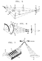
- FIG. 1 schematically depicts an electron beam, following its curved synchrotron path, and emitting a fan of x-ray radiation.
- FIG. 2 is a plan view of a projection mask being scanned by the arc-shaped illumination field of a ringfield camera.
- FIGs. 3A and 3B show a multi-faceted mirror, collecting an arc of synchrotron radiation, for delivery to a focus.
- FIGs. 4A and 4B show use of a "stacked collector" - of a collector yielding overlapping parallel radiation fans.
- FIG. 5 shows converging optics for processing separated fans of radiation into a horizontally merged illumination fan.
- FIG. 6 shows a multi-faceted collection mirror array yielding a stack of beams for full-field proximity imaging.
- FIG. 7 shows use of a 1-dimensional scatter plate of multi-faceted design.
- FIG. 8 shows an alternative form of 1-dimensional scatter plate using a sinusoidally undulating surface.
- FIG. 9 shows one form of a 2-dimensional scatter plate, depending on reflection from pyramidal surface protrusions.
- FIG. 10 is a schematic view of a condenser, provided with a collector, a real aperture and a scatter plate, for illuminating a projection mask.
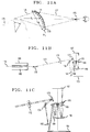
- FIGs. 11A, 11B and 11C are schematic views of the condenser of FIG. 10.
- FIG. 12 is a schematic view of a condenser of design alternative to that of FIGs. 10 and 11.
- FIG. 13 shows a synchrotron serving five device fabrication lines.
- FIGs. 14A and 14B are plan and elevational schematic representations of apparatus suitable for ringfield reduction projection.
- Synchrotron - Electron storage ring providing for relativistic electrons confined by magnetic fields to a repeating orbital path.
- Illuminating Radiation The delineating radiation as incident on and producing an Illumination Field on the mask, characterized by intensity, direction, divergence and spectral width.
- Divergence As used by itself, the term refers to mask divergence, i.e., the largest angle about the axis of the cone of radiation as incident on the mask. In projection, the axis is generally a few degrees off normal incidence as required for reflection masking. The magnitude of divergence required in projection is that needed to reduce ringing at feature edges to the extent necessary for desired resolution and contrast. In full-field exposure, divergence should be similar at every illumination point.
- Condenser Optical system for collecting radiation from the synchrotron, for processing the radiation into a form suitable for lithography, and for illuminating the mask.
- Collecting Optics or Collector
- Processing Optics Any optics, in addition to the collecting optics, within the condenser for processing collected radiation for delivery to the mask.
- Imaging Optics Optics following the condenser responsible for delivering mask-modulated radiation to the wafer, i.e. the camera optics.
- Camera Pupil Real or virtual aperture which defines the position through which illumination radiation must enter the camera, of angular size defining the diffraction limit of the camera. Its physical size is that of an image of the real limiting aperture of the camera.
- Lens The term is used in this description to define any optical element which causes x-ray radiation to converge or diverge. "Lenses", in x-ray systems, are generally reflecting - are sometimes referred to as "mirrors". Contemplated lenses may be multi-faceted or single-facet (continuous - e.g., of ellipsoidal or other curvature). The convergence or divergence is a result of an action analogous to that of a transmission optical lens.
- Individual facets may be planar or curved.
- Full-Field exposure - Simultaneous (rather than sequential) exposure of an area In its derivation, the term generally refers to a complete circuit pattern such as that of an entire chip. In this description, it is used to refer to any low-aspect ratio rectilinear pattern region, whether of an entire or partial pattern. Contemplated partial patterns may be stitched together by step-and-repeat to constitute the entire pattern.
- the advance makes effective use of x-ray synchrotron radiation, collected over a large emission arc for use in illuminating a pattern mask.
- the arc is at least 100 mrad, or preferably 200 mrad to a full radian or more.
- Pattern delineation to which the radiation is to be applied may take a variety of forms. It may take the form of full-field exposure or of a scanning region. Exposure may be by proximity printing, or by projection. A favored form of projection, known as ringfield projection, makes use of a scanning region of arcuate shape, likely with object-to-image reduction, perhaps by a ratio of 5:1, to permit use of more economical, larger-feature, masks.
- Synchrotron radiation is not well adapted to meet either ringfield or full-field needs. Synchrotron radiation is schematically shown in FIG. 1. As the high speed electrons within beam 10 follow a curved path 11 they emit a fan of electromagnetic radiation 12. The photon energy is determined by the electron energy and by the curvature of the electron path. Electron energies of 5 ⁇ 108 ev - 1 ⁇ 109 ev are useful for x-ray radiation at the 5 ⁇ - 150 ⁇ wavelength range of interest (for synchrotron designs in present use). The emitted radiation fan is very thin, perhaps 1mm thick, spreading to a thickness of a few mm at a distance of several meters from the synchrotron. The angle of the fan is the same as that of the bent emitting path.
- the invention provides for collection of a large arc of synchrotron radiation by use of one or more peripherally-placed faceted lens arrays. Illustrative work discussed in detail provides for collection over a full radian ( ⁇ 57 °). This two-order-of-magnitude increase in collection angle increases throughput. Specific needs are met by a variety of arrangements. Collected radiation may be reassembled in proximity printing to yield: a scanning slit; or, alternatively, to yield an illumination region of small aspect ratio for full-field patterning. Species of the invention provide for scanning (e.g. ringfield) or full-field projection.
- the Collector - It is convenient to first discuss the collector element - the element constituted of many mirror facets about the periphery of the synchrotron. It is expected that a least arc of collection will be 100 mrad, likely from 200 mrad to 1.5 rad.
- the emission spectrum is broad. It is desirably tailored to meet particular needs.
- Efficient operation of the condenser - minimization of unwanted heating caused by radiation which is relatively ineffective for resist exposure - is aided by spectral narrowing.
- An early element in the condenser - conveniently the collector - may use a multi-layer mirror (MLR) for this purpose.
- MLR multi-layer mirror
- a typical ringfield camera pass band may be 130 ⁇ 1.3 ⁇ . This band is determined by present multi-layer mirror technology. A reflectivity of 60-65% results from use of 40 successive Mo-Si layer pairs. Soft x-ray is also favored for surface reflection. Angles of incidence of 5 - 20° may result in reflectivity of 80-90%.
- the distance from the collector to the synchrotron orbit is typically 1-3m. Closer spacing may require submillimeter facets; larger spacing may require collectors of excessive size.
- Facets are sequentially positioned about the synchrotron orbit. They may be used in a variety of ways. They may produce a facet-by-facet illumination field. They may produce a line field with "non-sequential" facet illumination. They may produce "stacked" radiation, ultimately to yield a field of reduced aspect ratio. Stacked radiation is convenient for full-field illumination, either in proximity printing; or, as further processed, for projection printing.
- the Lagrange Invariant requires that the product of convergence angle, ⁇ , and the corresponding focus dimension equal or exceed the same product at the mask, if a dispersing element (a scatter plate) is to be avoided.
- the Lopez mirror is designed to focus radiation to a small dimension.
- the small focus may have too little divergence.
- It's Lagrange invariant may be too small to be easily used in projection printing.
- the converging nature of the Lopez is useful in providing greater collection angle so that, e.g., 10 Lopez facets may reflect 100 planar facets.
- the focus of the collector may correspond with a real aperture, or it may, itself, define a virtual aperture. Adjustability of a real aperture is useful in obtaining desired pupil fill.
- Processing Optics A purpose of the processing optics is to match the characteristics of the camera. Characteristically, a projection reduction camera operates with a divergence of 5 mrad-15 mrad. Shape and size of the imaging region, again the responsibility of this part of the illumination system, varies with the camera design.
- collector facets are designed to direct, to shape, or otherwise to define the illumination region - to the extent that the collector goes beyond focusing collected radiation - to this extent, the collector itself functions as processing optics.
- Collector emission of stacked radiation fans has been described. Use of the stacking to produce a low-aspect ratio field is an example of processing by the collector.
- Variation in facet tilt angle, as well as use of curved facets. may increase processing capability of the collector. Additional faceting, beyond that needed for defining the focus, may also be used for processing.
- the collector may increase divergence and may shape the field. In most projection systems, separate processing optics is preferred, if only to avoid undue complexity in collector design. Processing lenses may, again, be faceted, or may have an ellipsoidal or other continuously curved surface.
- FIG. 6 illustrates a condenser for use in full-field proximity printing.
- One processing lens stacks the collected radiation and improves parallelicity.
- the illumination region must be directed into the entrance pupil of the camera to the proper degree of fill. Fractional filling, e.g. 50% pupil-fill, minimizes edge diffraction and increases contrast.
- the mask 20 includes a rectilinear patterned region 21, rad region which is being swept horizontally (in direction 23) by an arc-shaped illumination region 22 which may be 2mm wide x 100mm long.
- the energy from the condenser must illuminate only region 22 and no other part of region 21.
- full-field exposure as distinguished from the scanning shown
- pattern and region 21 must be simultaneously illuminated.
- FIG. 3A is illustrative in providing for a multi-faceted collector lens 30.
- Facet 31 may be planar; may be several mm x several cm in size. Each facet receives radiation from a related spot in the orbital path 32, and each directs its reflected ray into focus 33.
- Faceted lenses contemplated for use in the inventive processes include at least 4 facets. For many purposes - particularly for projection delineation - faceted lenses may contain many more than 4 facets.
- a preferred structure for ringfield reduction projection may use 40 or more planar facets.
- FIG. 3B depicts an illustrative form of lens 30, in this instance, a monolithic body.
- FIGs. 4A and 4B illustrate use of a "stacked" collector. While facets continue to be arranged side-by-side about the storage ring, resulting beams are not side-by-side, but form a vertical stack of parallel fans.
- three separate beams 41, 42, 43 strike converging collector elements 44, 45, 46 to produce converging beams which overlap in region 47.
- Elements 44, 45 and 46 as depicted are arrays of multi-faceted mirrors.
- top and bottom beams 41 and 43 are reflected by long, thin mirrors 48, so that they are made parallel to beam 42.
- Airtight valves 49 preserve vacuum in the synchrotron.
- FIG. 4B is a schematic representation of parallel, overlapping radiation fans as produced at focus 50.
- Incoming beams 41, 42 and 43 are converging as entering the focus and are diverging when leaving. Divergence may provide for merger to produce an evenly illuminated field on the mask.
- FIG. 5 shows an arrangement for utilization of stacked radiation fans for side-by-side merger.
- emitted rays 51 are collected by converging lens 52 to result in focus 53, within aperture 54, and in horizontal merged fan 55.
- the figure includes valves 56 for maintaining vacuum.
- FIG. 6 shows a condenser designed for full-field proximity printing.
- x-ray fan 60 first strikes collector 61 to yield converging beam 62.
- Converging beam 62 are then assembled into parallel radiation fans by lens elements 68, which in turn illuminate mask 64 to produce a corresponding image on wafer 65.
- focus 63 is at a position beyond that of mask 64 (and beyond wafer 65 as well).
- This arrangement provides for the beam parallelicity desired for proximity printing.
- the distance between mask 64 and elements 68 is such as to assure overlap and constant intensity merger of the radiation fans.
- arrays 69 constituting collector 61 may be single element, e.g. may be of Lopez or other curved form.
- FIG. 7 shows one form of scatter-plate.
- the collected beam 70 strikes facets 71 in vertical scatter-plate 72 to illuminate mask 73, and to yield the desired fill at pupil 74.
- This plate introduces divergence to the vertical component of the beam as viewed by the pupil.
- FIG. 8 shows an alternate form of scatter-plate 80.
- Single-direction scatter is the consequence of undulating surface 81, with specific scatter determined by elevational variation 82 and undulating periodicity 83.
- This form is especially useful in making radiation in the horizontal fan more divergent, when the Lagrange invariant of the collector is smaller than that of the camera.
- lens 90 serves as a two-dimensional scatter plate.
- pyramid planar surfaces 91, 92, 93 and 94 it may perform as a phase-plate which is analogous to the quadripole (or quadrature) diffraction plate described for use in UV step-and-repeat patterning in co-pending U.S. Application SN 08/029,749, filed 3/11/93.
- Incoming collimated radiation is redirected by pyramidal surfaces 91, 92, 93 and 94.
- Other reflector shapes providing for various forms of radiation are described in this co-pending application.
- FIG. 10 is a schematic plan view of a complete condenser.
- E-beam 100 in following curved path 101, emits a fan of radiation 102, considered as the composite of rays 103 produced by point sources within arc 104.
- the fan of radiation is collected by collector 105 which produces converging rays 107a corresponding with facets 107.
- the fan of rays 107a is shaped by aperture plate 107; vertical divergence is introduced at scatter-plate 108; radiation 109 is focused by ellipsoidal mirror 110; to irradiate mask 111; and finally to produce the desired fill 112 within camera pupil 113.
- Mirror 110 may be multi-faceted or continuous.
- Example 1 - Parameters for a ringfield condenser are discussed on the basis of FIG. 10.
- the mask is viewed as being illuminated in the horizontal plane by a multiplicity of sources from along the stripe of illumination on the surface of processing mirror 110.
- Each point on the mirror has light reflecting from it with a range of angles ⁇ 2 which overlap on the mask, with the effect that every point on the mask has light reflecting from it with a range of angles ⁇ m , directed at, and partially filling the camera entrance pupil.
- a typical value for ⁇ m is 25 mrad.
- the faceted mirror M v is located at a distance D1 + D v 1 from the source.
- the vertical height of the beam at M v is therefore (D1 + D v 2 ) ⁇ v mm, where ⁇ v is the vertical opening angle of the radiation which is +1mrad.
- the example illustrates condenser design to match a particular camera.
- Figures 11A, 11B and 11C are plan, elevation, and detailed views of the condenser described above.
- the length of mirror 170 (mirror M1) is 1061mm
- the width of each facet 171 is 7.5mm (the width dimension of the out-of-plane facet surface is not shown in the 2-dimensional representation of this figure) and the entire mirror collects 0.6 radians.
- Each facet is required to be adjustable and is located close to the electron beam.
- mirror 170 The facets of mirror 170 (M1) reflect the beam upwards with a 10° reflection angle, and direct the light through the aperture 172 (aperture S1). Beyond S1 is the faceted mirror 173 (mirror M v ) which is located 7035mm distant from the source. Mirror M v reflects the beam downwards through about 135° onto mirror 174 (mirror M2). Mirror M v is made up of MLR facets to accommodate the large angle of incidence. The vertical beam height at mirror M v is approximately 14mm, and this may be reduced to a minimum of 2mm at the mask. Mirror M v may consist of 10 facets, each 1.4mm in width, to create an illumination field on the mask of width 1.4mm with some penumbral blurring on each.
- the mirror M2 is ellipsoidal to satisfy the large incoming beam and substantial off-axis imaging requirements.
- a suitable ellipsoid shape has an eccentricity of 0.96, a directrix of 2718mm and a grazing angle of 20 degrees. With this ellipsoidal shape and the noted distances, the mask is illuminated with approximately the correct arc shape of illumination for ringfield delineation.
- the throughput efficiency of this second illuminator arrangement is approximately 32% which is a little higher than the earlier illuminator example due to the smaller grazing angle on mirror M1.
- FIGs. 11B and 11C depict elements not clearly seen in FIG. 11A.
- the electron orbital path 175 as seen on FIG. 11A is determined by bending magnets 180 to result in x-ray irradiation 176.
- this now-converging radiation 177 passes through aperture 172 to have its path determined by mirrors 173 and 174 (M v and M2, respectively).
- mask 181 is irradiated to produce beam 182.
- Camera optics include (in succession as viewed by incoming beam 182) mirrors 183, 184, 185 and 186). (For detailed description, see co-pending U.S. Application SN 07/732,559, filed July 19, 1991). Finally, the reduced image is produced on wafer 187.
- Example 2 - FIG. 12 is discussed as a second example of collection and processing.
- the apparatus of this figure includes a condenser of design alternative to that of FIG. 10. Discussion is in terms of ringfield projection delineation.
- multi-faceted mirror 120 collects about 500 mrad of x-ray radiation and directs it at ellipsoidal mirror 121(M2).
- Mirror M2 focuses the radiation through the mask to form a focus at the center of the camera pupil.
- M2 also shapes the beam into the arc shape for illuminating the reflection mask.
- 122 Scatter plate 123(M3) located between M2 and the mask consists of a mirror with a rippled sinusoidal surface (see FIG. 8). Radiation reflecting from M3 has its divergence increased such that it fills the camera entrance pupil to the required ⁇ in the horizontal plane. The pupil filling factor is thus determined by the sinusoidal profile of the M3 scatter plate.
- the scatter plate is essentially a long period grating (e.g.
- the radiation is tightly collimated from the storage ring.
- the vertical divergence of the radiation is also increased by the scatter plate 123, this time with a sinusoidal rippled surface normal to the rippled surface scattering the radiation in the horizontal plane.
- Scatter plate 123 thus has a dimpled surface, the detailed shape of which determines how the pupil 125 is filled.
- FIG. 13 is a plan view showing a synchrotron serving five fabrication lines. Variations from line to line are intended to show alternative condenser designs. In real apparatus, it is likely that all lines served will be of the same general design.
- the figure shows a synchrotron 130 with curved path regions 131, 132, 133, 134, each defining a radius of curvature of 1.5 m. Regions 131, 133 and 134 are served by collectors 135, 136 and 137, each collecting a full radian of radiation. Collectors 135 and 136 are illustrated as consisting of faceted arrays (135A, 135B and 135C in the instance of array 135). Collector 137 is a single curved faceted array. Section 132 is showed as serving two production lines 132a and 132b each utilizing approximately 0.5 rad. In the instances of collectors 135 and 136 merging of radiation yielded by each of the individual arrays is accomplished by processing lenses 140 and 141, respectively.
- FIGs. 14A and 14B depict a synchrotron electron orbit 150, emitting rays 151, to produce a fan of radiation 152 which in turn is collected by multi-faceted mirror lens 153.
- the lens brings radiation to focus on the horizontal plane at 154.
- the beam continues to diverge on the vertical plane, to be focused on that dimension only by lens 155 which, similar to the apparatus of FIG. 7, has a vertical focus at or near to mask 156.
- lens 155 shapes the illumination field to the arcuate form 156.
- Lens 155 conveniently multi-faceted, functions both to focus radiation on or near the mask in the vertical plane, and to focus radiation in the horizontal plane with focus at the camera pupil 157 of camera 158.
- Camera 158 then produces the mask image 159 on wafer 160.
- Example 3 - Discussion is in terms of 0.1 ⁇ m design rule VLSI.
- a work station such as 133A in FIG. 13 might typically collect 65° of radiation (1.13 rad) from a 600 Mev synchrotron with a current of 700 ma.
- Such a fan of radiation contains 4 watts of power in the 2.5% band width 134 ⁇ ⁇ 1.7 ⁇ , of a quality SXPL projection camera.
- the condenser consisting of one multilayer mirror with reflectivity of 60% and 2 grazing incidence mirrors of reflectivity of 85% and some additional loss due to geometric effects, delivers 40% of the power, i.e. 1.6 watts of usable x-rays, to the mask.
- the camera delivers 7% of this power, or 112 milliwatts to the wafer.
- the wafer is coated with a resist that has a sensitivity of 20 millijoules/cm2, resulting in an exposure of about 5.5cm2 of silicon waver per second.
- the silicon wafers are 8 inches in diameter, with almost 300cm2 of usable area.
- the time spent of exposure of a wafer is 55 seconds.
- the work station is capable of exposing only 40 eight inch wafers per hour. Because of periodic shutdowns to refill the storage ring with electrons, the average is reduced to 35 wafers per hour.
- the processing of the wafer consists of many processing steps for fabrication of levels involving film deposition and growth, diffusion, ion implantation and various wet and dry etches, as well as the lithography performed by the x-ray projection camera.
- a critical step is the generation of contact windows.
- the process consists of 1) growth of 0.1 microns of thermal oxide, 2) deposition of 0.35 microns of oxide by LPCVD (Low Pressure Chemical Vapor Deposition), 3) coating the waver with resist, 4) exposure of the resist to the delineating radiation of the lithographic camera which produces a latent image of the contact window pattern in the resist, 5) development of the resist by chemical means, thus exposing the oxide below the resist, 6) etching through the oxide to the underlying silicon by dry etching, and 7) later depositing metal to contact the silicon and forming the metal, usually aluminum, into strips that connect the many contact holes, gates, external pads, etc. together to form a circuit.
- LPCVD Low Pressure Chemical Vapor Deposition
Landscapes
- Physics & Mathematics (AREA)
- Engineering & Computer Science (AREA)
- General Physics & Mathematics (AREA)
- Chemical & Material Sciences (AREA)
- Nanotechnology (AREA)
- Crystallography & Structural Chemistry (AREA)
- Theoretical Computer Science (AREA)
- Mathematical Physics (AREA)
- Condensed Matter Physics & Semiconductors (AREA)
- Manufacturing & Machinery (AREA)
- Computer Hardware Design (AREA)
- Microelectronics & Electronic Packaging (AREA)
- Power Engineering (AREA)
- Exposure And Positioning Against Photoresist Photosensitive Materials (AREA)
- Exposure Of Semiconductors, Excluding Electron Or Ion Beam Exposure (AREA)
Applications Claiming Priority (2)
| Application Number | Priority Date | Filing Date | Title |
|---|---|---|---|
| US59924 | 1979-07-23 | ||
| US08/059,924 US5439781A (en) | 1993-05-10 | 1993-05-10 | Device fabrication entailing synchrotron radiation |
Publications (1)
| Publication Number | Publication Date |
|---|---|
| EP0627667A1 true EP0627667A1 (en) | 1994-12-07 |
Family
ID=22026170
Family Applications (1)
| Application Number | Title | Priority Date | Filing Date |
|---|---|---|---|
| EP94303046A Withdrawn EP0627667A1 (en) | 1993-05-10 | 1994-04-27 | Device fabrication entailing synchrotron radiation |
Country Status (5)
| Country | Link |
|---|---|
| US (1) | US5439781A (ko) |
| EP (1) | EP0627667A1 (ko) |
| JP (1) | JP3429361B2 (ko) |
| KR (1) | KR100416862B1 (ko) |
| CA (1) | CA2121608C (ko) |
Cited By (13)
| Publication number | Priority date | Publication date | Assignee | Title |
|---|---|---|---|---|
| EP0741130A1 (de) * | 1993-12-14 | 1996-11-06 | Bayer Ag | Verfahren zur Herstellung von Sulfonen |
| WO1999000691A1 (en) * | 1997-06-30 | 1999-01-07 | Polaroid Corporation | Monolithic multi-faceted mirror for combining multiple beams from different light sources by reflection |
| EP1225481A2 (de) * | 2001-01-23 | 2002-07-24 | Carl Zeiss Semiconductor Manufacturing Technologies Ag | Kollektor für Beleuchtungssysteme mit einer Wellenlänge 193 nm |
| EP1284444A1 (en) * | 2001-08-15 | 2003-02-19 | ASML Netherlands B.V. | Lithographic apparatus and device manufacturing method |
| EP1333325A1 (en) * | 2002-02-01 | 2003-08-06 | Carl Zeiss Semiconductor Manufacturing Technologies Ag | Optical element for forming an arc-shaped illumination field |
| EP1037113A3 (en) * | 1999-03-12 | 2003-09-10 | ASML Netherlands B.V. | Illumination system for extreme ultraviolet radiation and its application in lithographic apparatus |
| WO2004092844A2 (de) * | 2003-04-17 | 2004-10-28 | Carl Zeiss Smt Ag | Optisches element für ein beleuchtungssystem |
| US6937316B2 (en) | 2001-08-15 | 2005-08-30 | Asml Netherlands B.V. | Lithographic apparatus, device manufacturing method and device manufactured thereby |
| US6947124B2 (en) | 1998-05-05 | 2005-09-20 | Carl Zeiss Smt Ag | Illumination system particularly for microlithography |
| KR100536631B1 (ko) * | 1999-03-12 | 2005-12-14 | 에이에스엠엘 네델란즈 비.브이. | 극자외선 방사선용 조명시스템 및 리소그래피투영장치에의 그 적용 |
| WO2014139815A1 (en) * | 2013-03-14 | 2014-09-18 | Carl Zeiss Smt Gmbh | Optical assembly for increasing the etendue |
| WO2016139055A3 (en) * | 2015-03-02 | 2016-10-27 | Asml Netherlands B.V. | Radiation system |
| US9955563B2 (en) | 2012-10-31 | 2018-04-24 | Carl Zeiss Smt Gmbh | EUV light source for generating a usable output beam for a projection exposure apparatus |
Families Citing this family (39)
| Publication number | Priority date | Publication date | Assignee | Title |
|---|---|---|---|---|
| KR0140472B1 (ko) * | 1994-10-12 | 1998-06-15 | 김주용 | 감광막 패턴 형성방법 |
| US5512759A (en) * | 1995-06-06 | 1996-04-30 | Sweatt; William C. | Condenser for illuminating a ringfield camera with synchrotron emission light |
| US5805365A (en) * | 1995-10-12 | 1998-09-08 | Sandia Corporation | Ringfield lithographic camera |
| US5691541A (en) * | 1996-05-14 | 1997-11-25 | The Regents Of The University Of California | Maskless, reticle-free, lithography |
| US6009143A (en) * | 1997-08-08 | 1999-12-28 | International Business Machines Corporation | Mirror for providing selective exposure in X-ray lithography |
| US5920380A (en) * | 1997-12-19 | 1999-07-06 | Sandia Corporation | Apparatus and method for generating partially coherent illumination for photolithography |
| EP0955641B1 (de) * | 1998-05-05 | 2004-04-28 | Carl Zeiss | Beleuchtungssystem insbesondere für die EUV-Lithographie |
| US7109497B2 (en) * | 1998-05-05 | 2006-09-19 | Carl Zeiss Smt Ag | Illumination system particularly for microlithography |
| US6859515B2 (en) * | 1998-05-05 | 2005-02-22 | Carl-Zeiss-Stiftung Trading | Illumination system, particularly for EUV lithography |
| US6947120B2 (en) * | 1998-05-05 | 2005-09-20 | Carl Zeiss Smt Ag | Illumination system particularly for microlithography |
| DE19903807A1 (de) * | 1998-05-05 | 1999-11-11 | Zeiss Carl Fa | Beleuchtungssystem insbesondere für die EUV-Lithographie |
| US7186983B2 (en) | 1998-05-05 | 2007-03-06 | Carl Zeiss Smt Ag | Illumination system particularly for microlithography |
| US6438199B1 (en) | 1998-05-05 | 2002-08-20 | Carl-Zeiss-Stiftung | Illumination system particularly for microlithography |
| US6859328B2 (en) * | 1998-05-05 | 2005-02-22 | Carl Zeiss Semiconductor | Illumination system particularly for microlithography |
| DE19935404A1 (de) * | 1999-07-30 | 2001-02-01 | Zeiss Carl Fa | Beleuchtungssystem mit mehreren Lichtquellen |
| US7142285B2 (en) * | 1998-05-05 | 2006-11-28 | Carl Zeiss Smt Ag | Illumination system particularly for microlithography |
| USRE42065E1 (en) | 1998-05-05 | 2011-01-25 | Carl Zeiss Smt Ag | Illumination system particularly for microlithography |
| DE10100265A1 (de) * | 2001-01-08 | 2002-07-11 | Zeiss Carl | Beleuchtungssystem mit Rasterelementen unterschiedlicher Größe |
| US6858853B2 (en) * | 1998-05-05 | 2005-02-22 | Carl Zeiss Smt Ag | Illumination system particularly for microlithography |
| US7126137B2 (en) * | 1998-05-05 | 2006-10-24 | Carl Zeiss Smt Ag | Illumination system with field mirrors for producing uniform scanning energy |
| US20070030948A1 (en) * | 1998-05-05 | 2007-02-08 | Carl Zeiss Smt Ag | Illumination system with field mirrors for producing uniform scanning energy |
| US7329886B2 (en) * | 1998-05-05 | 2008-02-12 | Carl Zeiss Smt Ag | EUV illumination system having a plurality of light sources for illuminating an optical element |
| US20050002090A1 (en) * | 1998-05-05 | 2005-01-06 | Carl Zeiss Smt Ag | EUV illumination system having a folding geometry |
| US7006595B2 (en) * | 1998-05-05 | 2006-02-28 | Carl Zeiss Semiconductor Manufacturing Technologies Ag | Illumination system particularly for microlithography |
| USRE41667E1 (en) * | 1998-05-05 | 2010-09-14 | Carl Zeiss Smt Ag | Illumination system particularly for microlithography |
| US6210865B1 (en) * | 1998-08-06 | 2001-04-03 | Euv Llc | Extreme-UV lithography condenser |
| US6225027B1 (en) | 1998-08-06 | 2001-05-01 | Euv Llc | Extreme-UV lithography system |
| US6118577A (en) * | 1998-08-06 | 2000-09-12 | Euv, L.L.C | Diffractive element in extreme-UV lithography condenser |
| US6469827B1 (en) | 1998-08-06 | 2002-10-22 | Euv Llc | Diffraction spectral filter for use in extreme-UV lithography condenser |
| JP2000091220A (ja) | 1998-09-08 | 2000-03-31 | Nikon Corp | 投影露光装置及び投影露光方法 |
| US7248667B2 (en) * | 1999-05-04 | 2007-07-24 | Carl Zeiss Smt Ag | Illumination system with a grating element |
| DE19921597C1 (de) | 1999-05-07 | 2000-07-27 | Maier Zerkleinerungsanlage Gmb | Messerring-Zerspaner zum Zerspanen von Hackschnitzeln |
| EP1200879B1 (de) * | 1999-07-30 | 2007-06-20 | Carl Zeiss SMT AG | Steuerung der Beleuchtungsverteilung in der Austrittspupille eines EUV-Beleuchtungssystems |
| US6285737B1 (en) | 2000-01-21 | 2001-09-04 | Euv Llc | Condenser for extreme-UV lithography with discharge source |
| US6683319B1 (en) * | 2001-07-17 | 2004-01-27 | Mitec Incorporated | System and method for irradiation with improved dosage uniformity |
| US20050180013A1 (en) * | 2002-03-21 | 2005-08-18 | Carl Zeiss Smt Ag | Grating element for filtering wavelengths < 100 nm |
| JP4518078B2 (ja) * | 2004-09-22 | 2010-08-04 | 株式会社ニコン | 照明装置、露光装置及びマイクロデバイスの製造方法 |
| JP4989180B2 (ja) * | 2006-10-13 | 2012-08-01 | キヤノン株式会社 | 照明光学系および露光装置 |
| DE102008000967B4 (de) | 2008-04-03 | 2015-04-09 | Carl Zeiss Smt Gmbh | Projektionsbelichtungsanlage für die EUV-Mikrolithographie |
Citations (2)
| Publication number | Priority date | Publication date | Assignee | Title |
|---|---|---|---|---|
| US5003567A (en) * | 1989-02-09 | 1991-03-26 | Hawryluk Andrew M | Soft x-ray reduction camera for submicron lithography |
| WO1991014973A1 (en) * | 1990-03-22 | 1991-10-03 | British Technology Group Ltd | Mirrors |
Family Cites Families (5)
| Publication number | Priority date | Publication date | Assignee | Title |
|---|---|---|---|---|
| US5175755A (en) * | 1990-10-31 | 1992-12-29 | X-Ray Optical System, Inc. | Use of a kumakhov lens for x-ray lithography |
| JPH0527445A (ja) * | 1991-07-25 | 1993-02-05 | Mitsubishi Electric Corp | X線露光装置 |
| JP3202046B2 (ja) * | 1991-10-08 | 2001-08-27 | キヤノン株式会社 | 照明用光学装置 |
| US5235626A (en) * | 1991-10-22 | 1993-08-10 | International Business Machines Corporation | Segmented mask and exposure system for x-ray lithography |
| US5263073A (en) * | 1991-12-20 | 1993-11-16 | Board Of Supervisors Of Louisiana State University And Agricultural And Mechanical College | Scanning systems for high resolution E-beam and X-ray lithography |
-
1993
- 1993-05-10 US US08/059,924 patent/US5439781A/en not_active Expired - Lifetime
-
1994
- 1994-04-19 CA CA002121608A patent/CA2121608C/en not_active Expired - Fee Related
- 1994-04-27 EP EP94303046A patent/EP0627667A1/en not_active Withdrawn
- 1994-05-09 KR KR1019940010066A patent/KR100416862B1/ko not_active IP Right Cessation
- 1994-05-10 JP JP09535294A patent/JP3429361B2/ja not_active Expired - Lifetime
Patent Citations (2)
| Publication number | Priority date | Publication date | Assignee | Title |
|---|---|---|---|---|
| US5003567A (en) * | 1989-02-09 | 1991-03-26 | Hawryluk Andrew M | Soft x-ray reduction camera for submicron lithography |
| WO1991014973A1 (en) * | 1990-03-22 | 1991-10-03 | British Technology Group Ltd | Mirrors |
Non-Patent Citations (3)
| Title |
|---|
| H. SHIMANO ET AL.: "Design Optimization of Synchrotron Radiation Lithography Beamline for a Compact Storage Ring", JAPANESE JOURNAL OF APPLIED PHYSICS, vol. 31 PART1, no. 12B, December 1992 (1992-12-01), TOKYO JP, pages 4185 - 4188, XP000415421 * |
| R. LOPEZ-DELGARDO ET AL.: "FOCUSING ALL THE SYNCHROTRON RADIATION (2 PI RADIANS) FROM AN ELECTRON STORAGE RING ON A SINGLE POINT WITHOUT TIME DISTORTION", OPTICS COMMUNICATIONS, vol. 19, no. 2, November 1976 (1976-11-01), AMSTERDAM NL, pages 286 - 291, XP026233981, DOI: doi:10.1016/0030-4018(76)90362-X * |
| R.P. HAELBICH ET AL.: "SYNCHROTRON RADIATION X-RAY LITHOGRAPHY", NUCLEAR INSTRUMENTS & METHODS IN PHYSICS RESEARCH, vol. 222, 1984, AMSTERDAM NL, pages 291 - 301, XP001394744 * |
Cited By (26)
| Publication number | Priority date | Publication date | Assignee | Title |
|---|---|---|---|---|
| EP0741130A1 (de) * | 1993-12-14 | 1996-11-06 | Bayer Ag | Verfahren zur Herstellung von Sulfonen |
| US5663442A (en) * | 1993-12-14 | 1997-09-02 | Bayer Aktiengesellschaft | Process for the preparation of sulphones |
| US5675040A (en) * | 1993-12-14 | 1997-10-07 | Bayer Aktiengesellschaft | Process for the preparation of sulphones |
| WO1999000691A1 (en) * | 1997-06-30 | 1999-01-07 | Polaroid Corporation | Monolithic multi-faceted mirror for combining multiple beams from different light sources by reflection |
| US5933278A (en) * | 1997-06-30 | 1999-08-03 | Polaroid Corporation | Monolithic multi-faceted mirror for combining multiple beams from different light sources by reflection |
| US6947124B2 (en) | 1998-05-05 | 2005-09-20 | Carl Zeiss Smt Ag | Illumination system particularly for microlithography |
| EP1037113A3 (en) * | 1999-03-12 | 2003-09-10 | ASML Netherlands B.V. | Illumination system for extreme ultraviolet radiation and its application in lithographic apparatus |
| KR100536631B1 (ko) * | 1999-03-12 | 2005-12-14 | 에이에스엠엘 네델란즈 비.브이. | 극자외선 방사선용 조명시스템 및 리소그래피투영장치에의 그 적용 |
| EP1225481A2 (de) * | 2001-01-23 | 2002-07-24 | Carl Zeiss Semiconductor Manufacturing Technologies Ag | Kollektor für Beleuchtungssysteme mit einer Wellenlänge 193 nm |
| US7460212B2 (en) | 2001-01-23 | 2008-12-02 | Carl-Zeiss Smt Ag | Collector configured of mirror shells |
| US7244954B2 (en) | 2001-01-23 | 2007-07-17 | Carl Zeiss Smt Ag | Collector having unused region for illumination systems using a wavelength ≦193 nm |
| EP1225481A3 (de) * | 2001-01-23 | 2006-03-29 | Carl Zeiss SMT AG | Kollektor für Beleuchtungssysteme mit einer Wellenlänge 193 nm |
| US6937316B2 (en) | 2001-08-15 | 2005-08-30 | Asml Netherlands B.V. | Lithographic apparatus, device manufacturing method and device manufactured thereby |
| EP1284444A1 (en) * | 2001-08-15 | 2003-02-19 | ASML Netherlands B.V. | Lithographic apparatus and device manufacturing method |
| WO2003065123A1 (en) * | 2002-02-01 | 2003-08-07 | Carl Zeiss Smt Ag | Optical element for forming an arc-shaped field |
| EP1333325A1 (en) * | 2002-02-01 | 2003-08-06 | Carl Zeiss Semiconductor Manufacturing Technologies Ag | Optical element for forming an arc-shaped illumination field |
| WO2004092844A2 (de) * | 2003-04-17 | 2004-10-28 | Carl Zeiss Smt Ag | Optisches element für ein beleuchtungssystem |
| CN1774675B (zh) * | 2003-04-17 | 2010-10-20 | 卡尔蔡司Smt股份公司 | 用于照明系统的光学元件 |
| WO2004092844A3 (de) * | 2003-04-17 | 2005-08-11 | Zeiss Carl Smt Ag | Optisches element für ein beleuchtungssystem |
| US9955563B2 (en) | 2012-10-31 | 2018-04-24 | Carl Zeiss Smt Gmbh | EUV light source for generating a usable output beam for a projection exposure apparatus |
| WO2014139815A1 (en) * | 2013-03-14 | 2014-09-18 | Carl Zeiss Smt Gmbh | Optical assembly for increasing the etendue |
| TWI618987B (zh) * | 2013-03-14 | 2018-03-21 | 卡爾蔡司Smt有限公司 | 增加光展量的光學組件 |
| CN105143981B (zh) * | 2013-03-14 | 2018-04-03 | 卡尔蔡司Smt有限责任公司 | 增加光展量光学组件 |
| CN105143981A (zh) * | 2013-03-14 | 2015-12-09 | 卡尔蔡司Smt有限责任公司 | 增加光展量光学组件 |
| WO2016139055A3 (en) * | 2015-03-02 | 2016-10-27 | Asml Netherlands B.V. | Radiation system |
| US10580546B2 (en) | 2015-03-02 | 2020-03-03 | Asml Netherlands B.V. | Radiation system |
Also Published As
| Publication number | Publication date |
|---|---|
| CA2121608A1 (en) | 1994-11-11 |
| KR100416862B1 (ko) | 2004-04-29 |
| JP3429361B2 (ja) | 2003-07-22 |
| CA2121608C (en) | 2000-01-18 |
| JPH06333798A (ja) | 1994-12-02 |
| US5439781A (en) | 1995-08-08 |
| KR940027066A (ko) | 1994-12-10 |
Similar Documents
| Publication | Publication Date | Title |
|---|---|---|
| US5439781A (en) | Device fabrication entailing synchrotron radiation | |
| US5339346A (en) | Device fabrication entailing plasma-derived x-ray delineation | |
| US5512759A (en) | Condenser for illuminating a ringfield camera with synchrotron emission light | |
| US6118577A (en) | Diffractive element in extreme-UV lithography condenser | |
| US6285737B1 (en) | Condenser for extreme-UV lithography with discharge source | |
| JP3771414B2 (ja) | リソグラフ投影装置 | |
| US20060132747A1 (en) | Optical element for an illumination system | |
| EP0424134B1 (en) | X-ray exposure apparatus | |
| KR19990088055A (ko) | Euv리소그래피용조광시스템 | |
| US7133489B2 (en) | X-ray illumination optical system and X-ray reduction exposure apparatus | |
| JP2000003858A (ja) | 照明システム | |
| US7183565B2 (en) | Source multiplexing in lithography | |
| US5394451A (en) | Optical arrangement for exposure apparatus | |
| US6225027B1 (en) | Extreme-UV lithography system | |
| US6210865B1 (en) | Extreme-UV lithography condenser | |
| US6280906B1 (en) | Method of imaging a mask pattern on a substrate by means of EUV radiation, and apparatus and mask for performing the method | |
| US5949844A (en) | Exposure apparatus | |
| Hector et al. | Simultaneous optimization of spectrum, spatial coherence, gap, feature bias, and absorber thickness in synchrotron‐based x‐ray lithography | |
| EP1204888A1 (en) | Collimator and focusing optic | |
| JP2002532895A (ja) | Euv照射システム | |
| White et al. | Soft x-ray projection lithography: experiments and practical printers | |
| JP3794442B2 (ja) | 照明装置および露光装置 | |
| WO2003034476A1 (fr) | Procede de realisation de dessin, masque, et procede de fabrication de masque | |
| Sweatt et al. | Diffractive element in extreme-UV lithography condenser | |
| JP2005005729A (ja) | X線縮小投影露光方法、x線縮小投影露光装置及びこれを用いた半導体デバイス製造方法 |
Legal Events
| Date | Code | Title | Description |
|---|---|---|---|
| PUAI | Public reference made under article 153(3) epc to a published international application that has entered the european phase |
Free format text: ORIGINAL CODE: 0009012 |
|
| AK | Designated contracting states |
Kind code of ref document: A1 Designated state(s): DE FR GB IT |
|
| 17P | Request for examination filed |
Effective date: 19950524 |
|
| 17Q | First examination report despatched |
Effective date: 19971211 |
|
| STAA | Information on the status of an ep patent application or granted ep patent |
Free format text: STATUS: THE APPLICATION IS DEEMED TO BE WITHDRAWN |
|
| 18D | Application deemed to be withdrawn |
Effective date: 20021105 |
|
| REG | Reference to a national code |
Ref country code: HK Ref legal event code: WD Ref document number: 1006369 Country of ref document: HK |