EP0626728B1 - Circuit integré du type à résistance, capacité et transistor, procédé de fabrication d'un tel circuit intégré et application à un oscillateur - Google Patents
Circuit integré du type à résistance, capacité et transistor, procédé de fabrication d'un tel circuit intégré et application à un oscillateur Download PDFInfo
- Publication number
- EP0626728B1 EP0626728B1 EP94401162A EP94401162A EP0626728B1 EP 0626728 B1 EP0626728 B1 EP 0626728B1 EP 94401162 A EP94401162 A EP 94401162A EP 94401162 A EP94401162 A EP 94401162A EP 0626728 B1 EP0626728 B1 EP 0626728B1
- Authority
- EP
- European Patent Office
- Prior art keywords
- bar
- diffusion
- type
- terminal
- integrated circuit
- Prior art date
- Legal status (The legal status is an assumption and is not a legal conclusion. Google has not performed a legal analysis and makes no representation as to the accuracy of the status listed.)
- Expired - Lifetime
Links
Images


Classifications
-
- H—ELECTRICITY
- H03—ELECTRONIC CIRCUITRY
- H03K—PULSE TECHNIQUE
- H03K3/00—Circuits for generating electric pulses; Monostable, bistable or multistable circuits
- H03K3/86—Generating pulses by means of delay lines and not covered by the preceding subgroups
-
- H—ELECTRICITY
- H03—ELECTRONIC CIRCUITRY
- H03K—PULSE TECHNIQUE
- H03K3/00—Circuits for generating electric pulses; Monostable, bistable or multistable circuits
- H03K3/02—Generators characterised by the type of circuit or by the means used for producing pulses
- H03K3/023—Generators characterised by the type of circuit or by the means used for producing pulses by the use of differential amplifiers or comparators, with internal or external positive feedback
- H03K3/0231—Astable circuits
-
- H—ELECTRICITY
- H10—SEMICONDUCTOR DEVICES; ELECTRIC SOLID-STATE DEVICES NOT OTHERWISE PROVIDED FOR
- H10D—INORGANIC ELECTRIC SEMICONDUCTOR DEVICES
- H10D84/00—Integrated devices formed in or on semiconductor substrates that comprise only semiconducting layers, e.g. on Si wafers or on GaAs-on-Si wafers
- H10D84/80—Integrated devices formed in or on semiconductor substrates that comprise only semiconducting layers, e.g. on Si wafers or on GaAs-on-Si wafers characterised by the integration of at least one component covered by groups H10D12/00 or H10D30/00, e.g. integration of IGFETs
- H10D84/811—Combinations of field-effect devices and one or more diodes, capacitors or resistors
Definitions
- the invention relates to an integrated circuit of the resistance, capacitance and transistor. She finds in particular an application in oscillators.
- RC type circuits are used in particular in relaxation oscillators. These oscillators indeed have a capacitance which is charged by means of a resistor and which is discharged by means of a transistor. The sizes of these three discrete elements directly influence the charge and discharge times of the capacity. In particular, the larger the capacity, the slower the discharge and the larger the discharge transistor for the discharge to take place as quickly as possible. In practice, the discharge is very dependent on the characteristics of the discrete elements (capacity, transistor). With current technologies, the discharge thus requires at least 2 to 5 nanoseconds for very large capacities of the order of 10 pF (10.10 -12 farads). However, the charge and discharge times have a direct influence on the frequency that the relaxation oscillator makes it possible to obtain. The frequency is therefore also dependent on the characteristics of the discrete charge and discharge elements and the minimum discharge time of the capacity limits the frequency. With current technologies, a maximum of 10 to 20 megahertz is thus obtained at the output of a relaxation oscillator.
- the subject of the invention is a circuit structure integrated resistance, capacitor and transistor which allows faster discharge and independent of sizes of resistance and ability. For a technology given, we have a very small and fixed discharge time, whatever the value of the capacity in particular.
- the structure of the invention is moreover advantageously compact.
- the first form of bar can be linear, folded into a serpentine, or wound in a helix according to the size and the desired length.
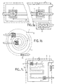
- the diffusion bar 1 N can be linear (Figure 1a), but also wound in a helix (Figure 1b) or still well folded into a serpentine (Figure 1c).
- the shape of the bar essentially depends on the length Lb envisaged for the bar and the space available for realize the circuit: folded or rolled up forms offer a much better compactness than the shape linear.
- connection terminals A, B The ends 2, 3 of the bar are connected to connection terminals A, B.
- connection of two ends of the bar are made of metal.
- two openings are provided in the plate polysilicon, at the location of the two ends 2, 3 of the bar 1 and through which the metallization is performed.
- the metallizations form a ribbon in a upper plane parallel to the polysilicon plate.
- connection could be made for example with a second level of polysilicon (circuits multi-poly).
- the polysilicon plate 4 is of the type rectangular (see square), as shown in the Figure 1c, or even circular ( Figure 1b). She is connected to a third connection terminal D. In the assembly shown, the plate is provided with a ribbon-shaped extension in the plane of the plate, which constitutes this third connection terminal D of the circuit ( Figure 1a, 1b, 1c). But we could also contact the polysilicon at a metallization for form this third terminal (not shown).
- connection terminal F The self-aligned diffusion 5 is also connected to a connection terminal F.
- this connection is made by a metallization which comes vertically ( Figure 2, step f) preferably at several points Pi, on the diffusion 5, from an upper plane parallel to the plate polysilicon, plane in which it forms a ribbon which constitutes the connection terminal F.
- connection terminals can be all in the same metallization plane above the polysilicon plate (as shown) or in different plans (circuit with several layers of metallization).
- the dopings used are those of the techniques classics for different types of delivery.
- the bar 1 produced according to a non-self-aligned method for example according to the method described above and commonly called the "capa-implant" method, there is typically a doping of impurities of 10 19 cm -3 which allows to have a resistivity per square of 100 ⁇ .
- Doping variants are possible which make it possible to increase the resistivity, up to a doping of 10 17 cm -3 which makes it possible to obtain a resistivity per square of 5 kilo-ohms.
- the bar is less doped (N +) than the self-aligned scattering (N ++ ).
- N + the self-aligned scattering
- N ++ the self-aligned scattering
- a typical drain or transistor source doping can be chosen (low energy ion implantation through a gate oxide), ie a doping of 10 20 cm -3 .
- the circuit obtained is a quadrupole A, B, D, F of resistance type, capacitance and transistor. But these elements are not discretizable, or separable: they are distributed along the diffusion bar N.
- An equivalent electronic model must include several elementary stages each comprising a resistance, capacitance and transistor, characterized by average values.
- the resistance per tile is of the order of 100 ⁇ / ⁇ .
- the distributed capacity is formed by the distributed capacity C1 of the bar / substrate junction as well as the distributed capacity C2 bar / polysilicon.
- the distributed transistor has in particular as minimum length of the channel, the length of the bar under the polysilicon plate (Lb).
- the transistor gate Distributed T is formed by the polysilicon plate.
- Her source is connected to terminal F of the quadrupole.
- the circuit is indeed compact, since the three resistance, capacitance and transistor elements are obtained by the same structure and not by three different structures.
- the compactness can also be improved by using drawing tips like shown for example in Figure 1c, with a drop in the polysilicon at the level of the metallization of the self-aligned diffusion 5.
- one of the inverters is a trigger Schmitt with a low / high tilt threshold V1 different from the V2 high / low switching threshold.
- the discharge with the circuit of the invention is extremely fast because the elements are distributed throughout the bar. If the bar is long, the capacity is large but the transistor equivalent is also very broad.
- the discharge time is always the same, in a given technology (doping), on the order of a nanosecond.
- VCC 5 volts
- V1 of around 4 volts and V2 around 1 volt we have 45 nanoseconds of charge and 1 nanosecond of discharge.
- the dimensions R, C influence the charging time. But the discharge is however independent of the dimensions of R, C, T. We can then obtain a signal at OUT high frequency pulse.
Landscapes
- Semiconductor Integrated Circuits (AREA)
- Metal-Oxide And Bipolar Metal-Oxide Semiconductor Integrated Circuits (AREA)
- Inductance-Capacitance Distribution Constants And Capacitance-Resistance Oscillators (AREA)
Description
- une première diffusion de dopage d'un second type (N+) en forme de barreau de longueur Lb et de largeur e, pourvue en ses deux extrémités d'une première borne A et d'une deuxième borne B de connexion;
- une plaque de polysilicium qui recouvre le barreau et comportant un prolongement qui forme une troisième borne D de connexion;
- une deuxième diffusion de dopage du second type (N++), auto-alignée par la plaque de polysilicium et pourvue d'une quatrième borne F de connexion;
- la réalisation d'un barreau de diffusion de dopage élevé d'un deuxième type;
- la formation d'un oxyde de grille dans une fenêtre plus large que le barreau, délimitée par de l'oxyde épais;
- le recouvrement du barreau par une plaque de polysilicium;
- la réalisation d'une diffusion de dopage du même type que celui du barreau, cette diffusion étant auto-alignée par la plaque de polysilicium et délimitée par l'oxyde épais;
- la connexion de chaque extrémité du barreau à une première borne A et une deuxième borne B de connexion;
- la connexion de la plaque de polysilicium à une troisième borne de connexion D;
- la connexion de la diffusion auto-alignée à une quatrième borne de connexion F.
- un quadripôle A,B,D,F selon l'invention;
- un transistor de charge Tp mis en série entre une tension de charge Vcc et la borne A du quadripôle, avec sa grille connectée à la borne D du quadripôle;
- un étage de sortie ayant son entrée connectée à la borne B du quadripôle et sa sortie connectée à la borne D du quadripôle,
- la figure 1a représente un circuit quadripôle selon l'invention;
- la figure 1b représente une variante d'un circuit selon l'invention;
- la figure 1c représente une autre variante d'un circuit selon l'invention;
- la figure 2 représente en coupe différentes étapes a) à f) de fabrication d'un circuit selon l'invention;
- la figure 3 est un modèle électronique approximé du quadripôle de l'invention et
- la figure 4 représente un circuit oscillateur à relaxation utilisant le quadripôle de l'invention.
- une première diffusion N+ en forme de barreau 1 de longueur Lb et de largeur e, réalisée dans un substrat P. Les deux extrémités du barreau sont référencées 2, 3.
- Une plaque 4 de polysilicium qui recouvre le barreau 1 de diffusion.
- Une deuxième diffusion N++ référencée 5, auto-alignée par la plaque de polysilicium. on a alors de manière classique un oxyde mince (non représenté) sous la plaque de polysilicium et sur la diffusion auto-alignée.
- la réalisation d'un barreau de diffusion de type N selon un procédé non auto-aligné ;
- la formation d'un oxyde de grille dans une fenêtre plus large que le barreau, délimitée par de l'oxyde épais;
- le recouvrement du barreau par une plaque de polysilicium;
- la réalisation d'une diffusion de dopage du même type N que celui du barreau, cette diffusion étant auto-alignée par la plaque de polysilicium et délimitée par l'oxyde épais,
- la connexion de chaque extrémité 2, 3 du barreau 1 à une première borne A et une deuxième borne B de connexion;
- la connexion de la plaque de polysilicium à une troisième borne de connexion D;
- la connexion de la diffusion auto-alignée à une quatrième borne de connexion F.
- oxydation thermique du silicium (étape a);
- dépôt d'une couche de nitrure de silicium et gravure du nitrure et de l'oxyde (étape b);
- implantation ionique d'isolation de type P (Bore);
- croissance d'oxyde pour former l'oxyde de champ épais (étape c) ;
- retrait du nitrure;
- retrait de l'oxyde mince;
- masquage et implantation ionique de type N (Arsenic) pour former le barreau 1 de diffusion non auto-alignée (étape d);
- croissance de l'oxyde de grille;
- dépôt d'une couche de polysilicium et dopage de type N (phosphore) du polysilicium;
- photolithographie et gravure du polysilicium pour former la plaque 4 (avec les ouvertures pour les contacts sur le barreau);
- implantation ionique source-drain de type N (Arsenic) pour former la diffusion auto-alignée 5 (étape e) ;
- réoxydation;
- dépôt d'une couche d'oxyde d'isolation (vapox);
- ouverture des contacts dans la couche d'oxyde d'isolation;
- dépôt d'une couche de métal;
- gravure du métal (étape f);
- dépôt d'une couche de passivation et gravure de la couche de passivation.
- une résistance élémentaire Ri entre des noeuds Ai et Bi,
- une capacité élémentaire Ci1 de jonction barreau/substrat entre le noeud Bi et le substrat relié à la borne F,
- un transistor Ti entre le noeud Bi et le substrat, dont la grille est reliée à la plaque de polysilicium (borne D du quadripôle) et
- une capacité élémentaire Ci2 barreau/polysilicium entre le noeud Bi et la grille du transistor (borne D du quadripôle).
- lp = 25 µm
- Lp = 260 µm
- ld = 30 µm
- Ld = 270 µm
Ce=1,3(capacité C1)farad/□ +0,2(capacité C2) farad/□
- une capacité répartie totale C de 0,750.10-12 farad (donnée par C = Ce x Lb x e), pour des dimensions totales du circuit qui sont faibles de l'ordre de 900 µm2.
- un transistor Tp de type P en série entre la tension de charge Vcc et la borne A du quadripôle, sa grille étant connectée à la borne D du quadripôle;
- un étage de détection de seuil DET comprenant au moins deux inverseurs, en série entre la borne D et la borne B du quadripôle et délivrant une sortie OUT. La borne F du quadripôle est reliée à la masse.
- 0 volt sur la grille du transistor T réparti du quadripôle : il est bloqué;
- 0 volt sur la grille du transistor Tp de charge : il est donc passant et ramène la tension de charge Vcc sur la borne A du quadripôle : les capacités C1 et C2 formant la capacité répartie totale C se chargent à travers la résistance R répartie : la tension à la borne B monte et dépasse le seuil V1 bas/haut du détecteur qui bascule : sa sortie OUT passe à 5 volts (état logique haut ou "1"). On a donc 5 volts sur la borne D du quadripôle.
- 5 volts sur la grille du transistor Tp de charge; il est bloqué et la borne A est flottante.
- 5 volts sur la grille du transistor T réparti : il est passant. Les capacités C1 et C2 qui forment la capacité répartie totale C se déchargent à travers le transistor T réparti. La tension à la borne B du quadripôle diminue en-dessous du seuil V2 haut/bas du détecteur qui rebascule à zéro volt.
Claims (8)
- Circuit intégré du type comportant un substrat ou un caisson d'un premier type (P) de dopage et dans ce substrat ou ce caisson :une première diffusion de dopage d'un second type (N+) en forme de barreau (1) de longueur Lb et de largeur e, pourvue en ses deux extrémités (2,3) d'une première (A) et d'une deuxième (B) borne de connexion;une plaque de polysilicium (4) qui couvre entièrement le barreau (1) à l'exception des bornes de connexion et comportant un prolongement qui forme une troisième borne (D) de connexion;une deuxième diffusion (5) de dopage du second type (N++) auto-alignée par la plaque de polysilicium (4) et pourvue d'une quatrième borne (F) de connexion; le circuit intégré ainsi constitué formant un quadripôle A,B,D,F du type à résistance, capacité et transistor.
- Circuit intégré selon la revendication 1, caractérisé en ce que le barreau (1) est linéaire.
- Circuit intégré selon la revendication 1, caractérisé en ce que le barreau (1) est enroulé en hélice.
- Circuit intégré selon la revendication 1, caractérisé en ce que le barreau (1) est replié en serpentin.
- Circuit intégré selon la revendication 1, caractérisé en ce que le barreau (1) est moins dopé (N+) que la diffusion (5) auto-alignée (N++).
- Procédé de fabrication d'un circuit intégré dans un substrat ou un caisson d'un premier type de dopage caractérisé en ce qu'il comporte les étapes suivantes :la réalisation d'un barreau de diffusion non auto-alignée d'un deuxième type (1);la formation d'un oxyde de grille dans une fenêtre plus large que le barreau, délimitée par de l'oxyde épais;la réalisation d'une plaque de polysilicium (4) qui couvre entièrement le barreau de diffusion à l'exception des bornes de connexion;la réalisation d'une diffusion du deuxième type (5), cette diffusion étant auto-alignée par la plaque de polysilicium et délimitée par l'oxyde épais;la connexion de chaque extrémité du barreau à une première borne A et à une deuxième borne B de connexion;la connexion de la diffusion auto-alignée à une troisième borne de connexion (F);la connexion d'une quatrième borne (D) de connexion sur la plaque de polysilicium;
pour former un quadripôle A, B, D, F du type à résistance, capacité et transistor. - Oscillateur à relaxation comportant :cet étage de sortie fournissant un premier état logique en sortie pour une tension en entrée supérieure au seuil de détection et deuxième état logique en sortie pour une tension en entrée inférieure au seuil de détection.un quadripôle A, B, D, F selon la revendication 1un transistor de charge Tp mis en série entre une tension de charge Vcc et la borne A du quadripôle, avec sa grille connectée à la borne D du quadripôle;un étage de sortie DET avec au moins un seuil de détection, ayant son entrée connectée à la borne B du quadripôle et sa sortie OUT connectée à la borne D du quadripôle;
- Oscillateur à relaxation selon la revendication 7, caractérisé en ce que l'étage de sortie à un premier seuil de tension bas/haut (V1) et un deuxième seuil de tension haut/bas (V2).
Applications Claiming Priority (2)
| Application Number | Priority Date | Filing Date | Title |
|---|---|---|---|
| FR9306481 | 1993-05-28 | ||
| FR9306481A FR2705833B1 (fr) | 1993-05-28 | 1993-05-28 | Circuit intégré du type à résistance, capacité et transistor, procédé de fabrication d'un tel circuit intégré et application à un oscillateur. |
Publications (2)
| Publication Number | Publication Date |
|---|---|
| EP0626728A1 EP0626728A1 (fr) | 1994-11-30 |
| EP0626728B1 true EP0626728B1 (fr) | 2001-10-04 |
Family
ID=9447588
Family Applications (1)
| Application Number | Title | Priority Date | Filing Date |
|---|---|---|---|
| EP94401162A Expired - Lifetime EP0626728B1 (fr) | 1993-05-28 | 1994-05-25 | Circuit integré du type à résistance, capacité et transistor, procédé de fabrication d'un tel circuit intégré et application à un oscillateur |
Country Status (5)
| Country | Link |
|---|---|
| US (2) | US5430319A (fr) |
| EP (1) | EP0626728B1 (fr) |
| JP (1) | JPH0714930A (fr) |
| DE (1) | DE69428480T2 (fr) |
| FR (1) | FR2705833B1 (fr) |
Families Citing this family (5)
| Publication number | Priority date | Publication date | Assignee | Title |
|---|---|---|---|---|
| FR2705833B1 (fr) * | 1993-05-28 | 1995-06-30 | Sgs Thomson Microelectronics | Circuit intégré du type à résistance, capacité et transistor, procédé de fabrication d'un tel circuit intégré et application à un oscillateur. |
| US5977610A (en) * | 1998-10-21 | 1999-11-02 | National Semniconductor Corporation | Integrated circuit having resistor formed over multiple tubs of semiconductor material |
| FR2787922B1 (fr) | 1998-12-23 | 2002-06-28 | St Microelectronics Sa | Cellule memoire a programmation unique en technologie cmos |
| US6483168B1 (en) | 2001-09-13 | 2002-11-19 | National Semiconductor Corporation | Integrated circuit having resistor formed over emitter of vertical bipolar transistor |
| US20060261840A1 (en) * | 2005-05-18 | 2006-11-23 | Texas Instruments, Inc. | System and method for determining channel mobility |
Family Cites Families (6)
| Publication number | Priority date | Publication date | Assignee | Title |
|---|---|---|---|---|
| FR1424482A (fr) * | 1964-12-01 | 1966-01-14 | Csf | élément de circuit électrique intégré à réactance inductive |
| US3471755A (en) * | 1967-08-28 | 1969-10-07 | Sprague Electric Co | Distributed variable attenuator network |
| US3978431A (en) * | 1975-07-03 | 1976-08-31 | Motorola, Inc. | Temperature compensated oscillator |
| JPS5951141B2 (ja) * | 1977-03-10 | 1984-12-12 | 三洋電機株式会社 | 選局装置 |
| US4285001A (en) * | 1978-12-26 | 1981-08-18 | Board Of Trustees Of Leland Stanford Jr. University | Monolithic distributed resistor-capacitor device and circuit utilizing polycrystalline semiconductor material |
| FR2705833B1 (fr) * | 1993-05-28 | 1995-06-30 | Sgs Thomson Microelectronics | Circuit intégré du type à résistance, capacité et transistor, procédé de fabrication d'un tel circuit intégré et application à un oscillateur. |
-
1993
- 1993-05-28 FR FR9306481A patent/FR2705833B1/fr not_active Expired - Fee Related
-
1994
- 1994-05-19 US US08/246,070 patent/US5430319A/en not_active Expired - Lifetime
- 1994-05-25 DE DE69428480T patent/DE69428480T2/de not_active Expired - Fee Related
- 1994-05-25 EP EP94401162A patent/EP0626728B1/fr not_active Expired - Lifetime
- 1994-05-30 JP JP6139468A patent/JPH0714930A/ja not_active Withdrawn
-
1995
- 1995-03-08 US US08/399,900 patent/US5661324A/en not_active Expired - Lifetime
Non-Patent Citations (1)
| Title |
|---|
| Semiconductor Devices Physics & Technology S.M.Sze pub. J.Wiley 1985, pgs. 481-485 * |
Also Published As
| Publication number | Publication date |
|---|---|
| DE69428480D1 (de) | 2001-11-08 |
| FR2705833B1 (fr) | 1995-06-30 |
| DE69428480T2 (de) | 2002-05-08 |
| US5430319A (en) | 1995-07-04 |
| EP0626728A1 (fr) | 1994-11-30 |
| JPH0714930A (ja) | 1995-01-17 |
| US5661324A (en) | 1997-08-26 |
| FR2705833A1 (fr) | 1994-12-02 |
Similar Documents
| Publication | Publication Date | Title |
|---|---|---|
| EP0296997B1 (fr) | Structure de transistors MOS de puissance | |
| FR2741192A1 (fr) | Procede de conception et de fabrication de circuits integres et circuits integres realises selon ce procede | |
| FR2961016A1 (fr) | Circuit integre a dispositif de type fet sans jonction et a depletion | |
| FR2738079A1 (fr) | Dispositif a semiconducteurs, a tranchee, et procede de fabrication | |
| FR2597262A1 (fr) | Circuit integre a semi-conducteur avec condensateur de derivation associe a son cablage | |
| EP0140772A2 (fr) | Limiteur de puissance élevée à diodes PIN pour ondes millimétriques et procédé de réalisation des diodes | |
| EP0673068B1 (fr) | Dispositif de protection contre des surtensions dans des circuits intégrés | |
| EP0461967A2 (fr) | Composant semiconducteur à jonction Schottky pour amplification hyperfréquence et circuits logiques rapides, et procédé de réalisation d'un tel composant | |
| EP0392944B1 (fr) | Résistance spirale haute tension | |
| FR2694449A1 (fr) | Composant électronique multifonctions, notamment élément à résistance dynamique négative, et procédé de fabrication correspondant. | |
| EP0581702A1 (fr) | Condensateur en technologie CMOS | |
| FR2640081A1 (fr) | Transistor a effet de champ vertical | |
| EP0169122B1 (fr) | Elément à capacité variable, commandable par une tension continue | |
| EP0626728A1 (fr) | Circuit integré du type à résistance, capacité et transistor, procédé de fabrication d'un tel circuit intégré et application à un oscillateur | |
| EP1722422A2 (fr) | Circuit intégré comprenant une photodiode de type à substrat flottant et procédé de fabrication correspondant | |
| FR2818012A1 (fr) | Dispositif semi-conducteur integre de memoire | |
| FR2815774A1 (fr) | Resonateur electrique | |
| EP0958545B1 (fr) | Circuit integrateur de charges photogenerees a linearite amelioree | |
| FR2995139A1 (fr) | Transistor mos | |
| FR3093590A1 (fr) | Procédé de fabrication d’un élément capacitif, et circuit intégré correspondant. | |
| EP1274131A1 (fr) | Contact antistatique pour ligne en silicum polycristallin | |
| EP2369618A1 (fr) | Cellule memoire sram a quatre transistors munis d'une contre-electrode | |
| EP1670066A1 (fr) | Procédé de fabrication d'un circuit intégré comprenant un miroir enterré et ce circuit | |
| FR2738682A1 (fr) | Dispositif de protection contre des surtensions | |
| FR2561822A1 (fr) | Dispositif semi-conducteur a effet de champ a faible tension de dechet |
Legal Events
| Date | Code | Title | Description |
|---|---|---|---|
| PUAI | Public reference made under article 153(3) epc to a published international application that has entered the european phase |
Free format text: ORIGINAL CODE: 0009012 |
|
| 17P | Request for examination filed |
Effective date: 19940929 |
|
| AK | Designated contracting states |
Kind code of ref document: A1 Designated state(s): DE FR GB IT |
|
| 17Q | First examination report despatched |
Effective date: 19980316 |
|
| RAP3 | Party data changed (applicant data changed or rights of an application transferred) |
Owner name: STMICROELECTRONICS S.A. |
|
| GRAG | Despatch of communication of intention to grant |
Free format text: ORIGINAL CODE: EPIDOS AGRA |
|
| GRAG | Despatch of communication of intention to grant |
Free format text: ORIGINAL CODE: EPIDOS AGRA |
|
| GRAH | Despatch of communication of intention to grant a patent |
Free format text: ORIGINAL CODE: EPIDOS IGRA |
|
| GRAH | Despatch of communication of intention to grant a patent |
Free format text: ORIGINAL CODE: EPIDOS IGRA |
|
| GRAA | (expected) grant |
Free format text: ORIGINAL CODE: 0009210 |
|
| AK | Designated contracting states |
Kind code of ref document: B1 Designated state(s): DE FR GB IT |
|
| PG25 | Lapsed in a contracting state [announced via postgrant information from national office to epo] |
Ref country code: IT Free format text: LAPSE BECAUSE OF FAILURE TO SUBMIT A TRANSLATION OF THE DESCRIPTION OR TO PAY THE FEE WITHIN THE PRE;WARNING: LAPSES OF ITALIAN PATENTS WITH EFFECTIVE DATE BEFORE 2007 MAY HAVE OCCURRED AT ANY TIME BEFORE 2007. THE CORRECT EFFECTIVE DATE MAY BE DIFFERENT FROM THE ONE RECORDED.SCRIBED TIME-LIMIT Effective date: 20011004 |
|
| GBT | Gb: translation of ep patent filed (gb section 77(6)(a)/1977) |
Effective date: 20011004 |
|
| REF | Corresponds to: |
Ref document number: 69428480 Country of ref document: DE Date of ref document: 20011108 |
|
| RAP2 | Party data changed (patent owner data changed or rights of a patent transferred) |
Owner name: STMICROELECTRONICS S.A. |
|
| REG | Reference to a national code |
Ref country code: GB Ref legal event code: IF02 |
|
| PLBE | No opposition filed within time limit |
Free format text: ORIGINAL CODE: 0009261 |
|
| STAA | Information on the status of an ep patent application or granted ep patent |
Free format text: STATUS: NO OPPOSITION FILED WITHIN TIME LIMIT |
|
| 26N | No opposition filed | ||
| PGFP | Annual fee paid to national office [announced via postgrant information from national office to epo] |
Ref country code: DE Payment date: 20030605 Year of fee payment: 10 |
|
| PG25 | Lapsed in a contracting state [announced via postgrant information from national office to epo] |
Ref country code: DE Free format text: LAPSE BECAUSE OF NON-PAYMENT OF DUE FEES Effective date: 20041201 |
|
| PGFP | Annual fee paid to national office [announced via postgrant information from national office to epo] |
Ref country code: FR Payment date: 20050511 Year of fee payment: 12 |
|
| PGFP | Annual fee paid to national office [announced via postgrant information from national office to epo] |
Ref country code: GB Payment date: 20050525 Year of fee payment: 12 |
|
| PG25 | Lapsed in a contracting state [announced via postgrant information from national office to epo] |
Ref country code: GB Free format text: LAPSE BECAUSE OF NON-PAYMENT OF DUE FEES Effective date: 20060525 |
|
| GBPC | Gb: european patent ceased through non-payment of renewal fee |
Effective date: 20060525 |
|
| REG | Reference to a national code |
Ref country code: FR Ref legal event code: ST Effective date: 20070131 |
|
| PG25 | Lapsed in a contracting state [announced via postgrant information from national office to epo] |
Ref country code: FR Free format text: LAPSE BECAUSE OF NON-PAYMENT OF DUE FEES Effective date: 20060531 |