EP0625826B1 - Digitaler programmierbarer Frequenzteiler in einem Phasenregelkreis - Google Patents
Digitaler programmierbarer Frequenzteiler in einem Phasenregelkreis Download PDFInfo
- Publication number
- EP0625826B1 EP0625826B1 EP94104167A EP94104167A EP0625826B1 EP 0625826 B1 EP0625826 B1 EP 0625826B1 EP 94104167 A EP94104167 A EP 94104167A EP 94104167 A EP94104167 A EP 94104167A EP 0625826 B1 EP0625826 B1 EP 0625826B1
- Authority
- EP
- European Patent Office
- Prior art keywords
- output
- input
- coupled
- signal
- inverter
- Prior art date
- Legal status (The legal status is an assumption and is not a legal conclusion. Google has not performed a legal analysis and makes no representation as to the accuracy of the status listed.)
- Expired - Lifetime
Links
- 230000004044 response Effects 0.000 claims description 7
- 238000000034 method Methods 0.000 claims description 6
- 230000003111 delayed effect Effects 0.000 claims 5
- 238000001514 detection method Methods 0.000 description 14
- 230000007704 transition Effects 0.000 description 14
- 238000010586 diagram Methods 0.000 description 6
- 230000008569 process Effects 0.000 description 4
- 230000001934 delay Effects 0.000 description 3
- 238000007599 discharging Methods 0.000 description 3
- 238000012544 monitoring process Methods 0.000 description 2
- 238000005070 sampling Methods 0.000 description 2
- 239000003990 capacitor Substances 0.000 description 1
- 230000008859 change Effects 0.000 description 1
- 239000004020 conductor Substances 0.000 description 1
- 230000009977 dual effect Effects 0.000 description 1
- 230000000694 effects Effects 0.000 description 1
- 238000004519 manufacturing process Methods 0.000 description 1
- 238000012986 modification Methods 0.000 description 1
- 230000004048 modification Effects 0.000 description 1
- 238000012545 processing Methods 0.000 description 1
Images


Classifications
-
- H—ELECTRICITY
- H03—ELECTRONIC CIRCUITRY
- H03K—PULSE TECHNIQUE
- H03K23/00—Pulse counters comprising counting chains; Frequency dividers comprising counting chains
- H03K23/64—Pulse counters comprising counting chains; Frequency dividers comprising counting chains with a base or radix other than a power of two
- H03K23/66—Pulse counters comprising counting chains; Frequency dividers comprising counting chains with a base or radix other than a power of two with a variable counting base, e.g. by presetting or by adding or suppressing pulses
- H03K23/665—Pulse counters comprising counting chains; Frequency dividers comprising counting chains with a base or radix other than a power of two with a variable counting base, e.g. by presetting or by adding or suppressing pulses by presetting
-
- H—ELECTRICITY
- H03—ELECTRONIC CIRCUITRY
- H03L—AUTOMATIC CONTROL, STARTING, SYNCHRONISATION OR STABILISATION OF GENERATORS OF ELECTRONIC OSCILLATIONS OR PULSES
- H03L7/00—Automatic control of frequency or phase; Synchronisation
- H03L7/06—Automatic control of frequency or phase; Synchronisation using a reference signal applied to a frequency- or phase-locked loop
- H03L7/16—Indirect frequency synthesis, i.e. generating a desired one of a number of predetermined frequencies using a frequency- or phase-locked loop
- H03L7/18—Indirect frequency synthesis, i.e. generating a desired one of a number of predetermined frequencies using a frequency- or phase-locked loop using a frequency divider or counter in the loop
-
- Y—GENERAL TAGGING OF NEW TECHNOLOGICAL DEVELOPMENTS; GENERAL TAGGING OF CROSS-SECTIONAL TECHNOLOGIES SPANNING OVER SEVERAL SECTIONS OF THE IPC; TECHNICAL SUBJECTS COVERED BY FORMER USPC CROSS-REFERENCE ART COLLECTIONS [XRACs] AND DIGESTS
- Y10—TECHNICAL SUBJECTS COVERED BY FORMER USPC
- Y10S—TECHNICAL SUBJECTS COVERED BY FORMER USPC CROSS-REFERENCE ART COLLECTIONS [XRACs] AND DIGESTS
- Y10S331/00—Oscillators
- Y10S331/02—Phase locked loop having lock indicating or detecting means
Definitions
- the present invention relates in general to phase lock loops and, more particularly, to a programmable frequency divider in a phase lock loop for extending the pulse width of control signals to a lock detection circuit.
- Phase lock loops are found in a myriad of electronic applications such as modems and clock synchronization circuits for computer systems.
- a conventional PLL includes a phase detector for monitoring a phase difference between an input signal and an output signal of a voltage controlled oscillator (VCO).
- the phase detector generates an up control signal and a down control signal for a charge pump to charge and discharge a loop filter at a loop node at the input of the VCO.
- the loop voltage developed across the loop filter determines the output frequency of the VCO.
- the up and down control signals driving the charge pump set the proper loop node voltage at the input of the VCO to maintain a predetermined phase relationship between the signals applied to the phase detector.
- phase lock It is common for the PLL to lose phase lock should the input signal fade or jump to a different frequency of operation.
- the out-of-lock state can be detected with a lock detection circuit and other system processing suspended until the PLL can re-establish phase lock.
- One lock detection scheme monitors the up control signal and the down control signal at the output of the phase detector to ascertain the lock status of the PLL. If the up control signal and down control signal are not pulsing, then loop node voltage remains substantially constant and the PLL should be in phase lock. When the up control signal and the down control signal are steadily generating pulses charging or discharging the loop filter to adjust the input voltage of the VCO, the loop must be in motion and thus out of phase lock.
- the conventional lock detection circuit may include a delay circuit comprising a string of serially coupled inverters designed to ignore short intermittent pulses from the phase detector having less than a predetermined pulse width.
- the up and down control signals must have a pulse width as least as long as the delay circuit to trigger an out-of-lock condition.
- the pulse widths of the up and down control signals are subject to temperature and process variation and therefore are not well suited as control parameters for ascertaining phase lock.
- the pulse widths of the up and down control signals are merely rough indicators having limited accuracy of the true phase relationship between the input signals of the phase detector.
- a prior art programmable counter circuit is disclosed in EPO patent application 0474616A2.
- a variable divider circuit compares the contents of a pre-loaded binary counter with a constant value to provide a dual modulus counter.
- Another prior art programmable counter circuit is disclosed in EPO patent application 0498450A2. The contents of a latch are decremented to match the contents of a register and generate a serial clock that has a frequency and phase relationship with a received serial data stream.
- Another known lock detection scheme looks at the phase difference between the input signal and the output signal of the VCO as applied to the phase detector. If the transition of these signals occur outside a timeslot window, the loop is out of phase lock.
- the timeslot window is typically generated from the VCO output frequency and requires the input signal to have a 50% duty cycle since the lock detector checks both edges of the input signal.
- the timeslot window typically has a period equal to the period of the VCO output frequency. As the VCO output frequency increases past say 200 MHz, the width of the timeslot window may decrease to a point of becoming unusable. It is desirable to eliminate the requirement for an input signal with a 50% duty cycle and to provide a timeslot window having an extendible period independent of the VCO output frequency.
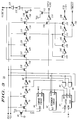
- a phase lock loop (PLL) 10 is shown in FIG. 1 suitable for manufacturing as an integrated circuit using conventional integrated circuit processes.
- a REFCLK signal operating at say 2.0 MHz is applied at input 12 at a first input of phase detector 14 to generate an UP control signal and a DOWN control signal for charge pump 16.
- Charge pump 16 may comprise a P-channel transistor and an N-channel transistor (not shown) serially coupled between a positive power supply conductor and ground potential, wherein the P-channel transistor is responsive to the UP control signal and the N-channel transistor is responsive to the DOWN control signal.
- the interconnection at the drains of the charge pump transistors drives loop node 18 for charging and discharging loop filter 22 which may comprise a capacitor (not shown) coupled between loop node 18 and ground potential.
- the voltage at loop node 18 controls VCO 24 for generating an oscillator signal OSCOUT at output 26.
- the OSCOUT signal of VCO 24 is applied to opposite phase clock generator 28 for developing non-overlapping, opposite phase clocks XCLK and YCLK.
- the XCLK and YCLK clock signals are divided through programmable frequency divider circuit 30 for providing an OSCOUT/N signal as applied at a second input of phase detector 14.
- Programmable divider circuit 30 also generates a TIMESLOT signal, a SAMPLE CLOCK signal and an XFER CLOCK signal for the lock detection feature of PLL 10.
- the operation of PLL 10 proceeds as follows.
- the REFCLK signal applied at the first input of phase detector 14 in combination with the OSCOUT/N signal applied at the second input of the same generates an UP control signal, or the DOWN control signal, according to the phase relationship therebetween.
- the UP control signal pulses if the OSCOUT/N signal lags the REFCLK signal, i.e., the frequency of the OSCOUT/N signal is too low relative to the REFCLK signal.
- the DOWN control signal pulses to reduce the frequency of the oscillator signal from VCO 24 if the OSCOUT/N signal leads the REFCLK signal.
- Charge pump 16 is responsive to the UP control signal and the DOWN control signal for charging and discharging loop node 18.
- phase detector 14 monitors the phase difference between the REFCLK signal and the OSCOUT/N signal and generates UP and DOWN control signals as necessary for charge pump 16 to drive loop node 18 and VCO 24 to maintain a predetermined phase relationship between the REFCLK and OSCOUT/N signals.
- Opposite phase clock generator 28 is shown in FIG. 2 where OSCOUT is applied through inverters 32, 33, 34 and 36 to a first input of AND gate 38.
- the output of inverter 32 is coupled through inverters 40 and 42 to a first input of AND gate 44.
- the output of AND gate 38 provides the XCLK clock signal as applied through inverter 46 to a second input of AND gate 44.
- the output of AND gate 44 provides the YCLK clock signal as applied through inverter 48 to a second input of AND gate 38.
- the output of inverter 34 at node 50 is coupled through inverter 52 to the input of inverter 42, while the output of inverter 40 at node 54 is coupled through inverter 56 to the input of inverter 36.
- inverter 40 attempts to switch node 54 to logic zero before node 50 switches to logic one because node 54 is only two inverter delays away from OSCOUT while node 50 is three inverter delays away. However, the transition of node 54 to logic zero is slowed by inverter 52 because node 50 is still logic zero two inverter delays after OSCOUT changes to logic zero. Inverter 52 acts to hold node 54 at logic one until the output of inverter 34 changes state.
- OSCOUT switches to logic one.
- the transition of inverters 36 and 42 overlap 180 ° out-of-phase and cross approximately at the 50% mark, thereby overcoming the delay difference imposed by an unequal number of inverters between OSCOUT and nodes 50 and 54.
- the XCLK clock signal at the output of AND gate 38 goes to logic zero.
- AND gate 44 receives logic ones from the outputs of inverters 42 and 46 for providing a logic one YCLK clock signal.
- the YCLK clock signal goes to logic zero.
- AND gate 38 receives logic ones from the output of inverters 36 and 48 for providing a logic one XCLK clock signal.
- the XCLK and YCLK clock signals are non-overlapping and opposite phase switching at substantially the 50% mark and operating at the frequency of OSCOUT.
- OSCOUT and XCLK signals operate in-phase.
- programmable frequency divider circuit 30 including latch 60 having first and second inputs IN1 and IN2 receiving the program integer N and an output from decrement circuit 62, respectively.
- the output of latch 60 is coupled to an input of decrement circuit 62 and the IN1 input of compare circuit 64.
- the IN2 input of compare circuit 64 receives a constant integer K.
- Transistor 66 operates as a pull-up device at the output of compare circuit 64.
- the gate of transistor 66 receives ground potential, while the source of transistor 66 receives power supply potential V DD operating at say 5.0 volts.
- the output signal from compare circuit 64 passes through transistor 68, inverter 70, transistor 72 and inverter 74 to node 76 in response to the XCLK and YCLK clock signals applied at the gates of transistors 68 and 72, respectively.
- Inverter 80 has an input coupled to node 76 and an output coupled to node 82.
- AND gate 84 has one input coupled to node 76 while its second input receives the XCLK clock signal.
- AND gate 86 has one input coupled to node 82 while its second input receives the XCLK clock signal.
- the outputs of AND gates 84 and 86 are coupled to the LD1 and LD2 load inputs of latch 60, respectively.
- the PASS input of latch 60 receives the YCLK clock signal.
- programmable divider circuit 30 may be set to divide the 200 MHz XCLK and YCLK clock signals by say integer one-hundred. Accordingly, program integer N is set equal to ninety-nine (one less than one-hundred), i.e., "1100011”.
- Compare circuit 64 produces a logic one FLAG pulse every one-hundredth OSCOUT clock cycle. The period of the FLAG pulse is the same as the period of OSCOUT.
- the FLAG pulse is lengthened by a delay circuit (114-138) to achieve the desired pulse width (at least one XCLK clock cycle) for TIMESLOT and XFER CLOCK signals.
- a logic one XCLK clock signal turns on transistor 68 and passes the logic one to inverter 70.
- the next logic one YCLK clock signal turns on transistor 72 and passes a logic zero from inverter 70 to inverter 74.
- node 76 goes to logic one and node 82 goes to logic zero following one period of the XCLK and YCLK clock signals after FLAG becomes logic one.
- the LD1 input of latch 60 receives a logic one from AND gate 84 at the following logic one XCLK clock signal to load the program integer N from the IN1 input.
- Latch 60 now contains integer "1100011” and provides the same integer at its OUT output after the next logic one YCLK clock signal.
- Decrement circuit 62 receives the "1100011" from latch 60 and performs a decrement of one each period of the XCLK and YCLK clock signals.
- FIG. 4 An embodiment of latch 60 is shown in FIG. 4 where the gates of transistors 90 and 92 receive the LD1 and LD2 inputs respectively.
- the sources of transistors 90 and 92 are coupled together to the input of inverter 94.
- Pass transistor 96 is coupled between the output of inverter 94 and the input of inverter 98 and operates in response to the PASS input of latch 60.
- transistor 90 passes the logic state applied at the IN1 input to inverter 94.
- a logic one YCLK clock signal enables transistor 96 to pass the inverted logic state from inverter 94 to produce the same logic state at the OUT output of latch 60 as applied at the IN1 input.
- Latching circuit 90-98 may latch the least significant bit of the applied digital signal.
- a latching circuit like 90-98 is provided for each bit of the digital signal applied thereto.
- An embodiment of compare circuit 64 is illustrated in FIG. 5 as exclusive-OR gate 100, transistor 102, exclusive-OR gate 104 and transistor 106.
- the comparing circuit 100-102 compares the least significant BIT 0 of the applied digital signals, while comparing circuit 104-106 compares the second least significant BIT 1.
- Transistor 106 turns on and pulls the OUT output of compare circuit 64 to logic zero.
- the drains of transistors 102 and 106 are coupled together so that only one mismatch between the output signal of latch 60 and the integer K causes a logic zero FLAG.
- the logic zero FLAG passes through transistors 68 and 72 and inverters 70 and 74 during the subsequent period of the XCLK and YCLK clock signals.
- Node 76 goes to logic zero and node 82 goes to logic one.
- the next logic one XCLK clock signal produces a logic one at the output of AND gate 86 and enables the IN2 input of latch 60.
- the "1100011” having been decremented by one to "1100010" in decrement circuit 62 during the previous period of the XCLK and YCLK clock signals is loaded into latch 60 and passes to decrement circuit 62 and compare circuit 64.
- the value "1100010” is again decremented by decrement circuit 62 during the following period of the XCLK and YCLK clock signals.
- FLAG remains logic zero since the digital signals still do not match.
- Nodes 76 and 82 remain at logic zero and logic one, respectively.
- the logic one FLAG passes through transistors 68 and 72 and inverters 70 and 74 during the following period of the XCLK and YCLK clock signals.
- Node 76 goes to logic one and node 82 goes to logic zero.
- the logic zero at node 82 passes through transistor 108 during the second high state of the XCLK clock signal after the FLAG pulse becomes logic one.
- Inverter 110 complements the signal to produce a logic one SAMPLE CLOCK output signal at the gate of transistor 112.
- Transistor 112 turns on to pull the input of inverter 114 to logic one as the OSCOUT/N output signal at the output of inverter 116 goes to logic one.
- the new latch value passes to compare circuit 64 at the next high state of the YCLK clock signal after node 76 goes to logic one.
- a comparison of the new latch value and the integer K yields a mismatch and the FLAG signal returns to logic zero.
- Nodes 76 and 82 switch back to logic zero and logic one, respectively, during the following period of the XCLK and YCLK clock signals to repeat the aforedescribed process.
- programmable divider circuit 30 produces a logic one FLAG pulse having the same pulse width as OSCOUT once every Nth cycle of OSCOUT.
- transistor 118 turns on during the following high state of the XCLK clock signal after node 82 goes to logic zero to pass the logic zero state to inverter 120.
- Inverter 120 complements the signal and passes it through transistor 122 during the high state of the YCLK clock signal where inverter 124 complements the signal again.
- the logic zero from inverter 124 passes through transistor 126 during another high state of the XCLK clock signal.
- Inverter 128 complements the signal and passes it through transistor 130 during another high state of the YCLK clock signal where inverter 132 complements the signal again.
- the next high state of the XCLK clock signal pass the logic zero from inverter 132 through transistor 134 and produces a logic one at the output of inverter 136.
- Transistor 138 turns on and pulls the input of inverter 114 to logic zero.
- node 82 has switched back to logic one and turned off transistor 112.
- the OSCOUT/N output signal goes to logic zero following inverter 116.
- Transistors 118, 122, 126, 130 and 134 and inverters 120, 124, 128, 132 and 136 operate as a delay circuit to lengthen the logic zero state of the OSCOUT/N signal. The delay may be adjusted by providing more or less transistor-inverter pairs between node 82 and the gate of transistor 138.
- the OSCOUT/N signal also passes through transistor 140 during the high state of the YCLK clock signal where it is complemented by inverter 142.
- Transistor 146 passes the complemented signal to inverter 148 during the next high state of the XCLK clock signal.
- the output signal of inverter 148 provides the TIMESLOT output signal after inversion by inverter 150.
- the output signal of inverter 148 also passes through transistor 152 during another high state of the YCLK clock signal.
- Inverter 154 complements the signal and passes it though transistor 156 during another high state of the XCLK clock signal.
- Inverter 158 provides the XFER CLOCK output signal at its output.
- Transistors 140, 146, 152 and 156 and inverters 142, 148, 150, 154 and 158 operate to center the TIMESLOT about the zero-going (logic one-to-logic zero) transition of OSCOUT/N with the XFER CLOCK signal occurring one XCLK and YCLK clock period later.
- Transistors 140 and 146 and inverters 142, 148 and 150 operate to widen the TIMESLOT pulse.
- the REFCLK signal and the OSCOUT/N signal are applied at the first and second inputs of lock detection circuit 160.
- the TIMESLOT signal from programmable divider circuit 30 is also applied to lock detector circuit 160 for generating a DETECT signal when the REFCLK signal and OSCOUT/N signal are logic one at the time of the zero-going transition of the TIMESLOT signal and logic zero at the time of the positive-going transition of the TIMESLO T window.
- the TIMESLOT window is defined as the low state of the TIMESLOT signal.
- the DETECT signal from lock detection circuit 160 is applied at the data input of 4-bit master/slave shift register 164 while the SAMPLE CLOCK and XFER CLOCK signals from programmable divider circuit 30 are applied at the clock inputs of the same.
- the SAMPLE CLOCK latches the input data in a master section of shift register 164 while the XFER CLOCK transfers the data to a slave section.
- the overall effect is to shift data between adjacent bit locations.
- Shift register 164 includes a tap point at each bit position coupled to the inputs of AND gate 166 for providing a LOCK signal at output 168. It takes only one false DETECT signal (logic zero) shifting into shift register 164 to drive the LOCK signal low indicating a out-of-lock condition.
- the DETECT signal must return to the true state (logic one) for at least four SAMPLE CLOCK and XFER CLOCK periods to completely shift the logic zero out of 4-bit shift register 164 and re-establish a true state for the LOCK signal. It is understood that shift register 164 can be made wider, say 12 bits or more, to increase the number of consecutive true DETECT signals necessary to issue a true LOCK signal.
- lock detector circuit 160 is shown in FIG. 6, wherein the REFCLK signal and the OSCOUT/N signal are applied at first and second inputs of NAND gate 170.
- the output of NAND gate 170 is coupled to the drain of transistor 172 which includes a gate coupled for receiving the TIMESLOT signal.
- the source of transistor 172 is coupled through inverters 174 and 176 to a first input of NOR gate 178.
- the REFCLK signal and the OSCOUT/N signal are applied at second and third inputs of NOR gate 178.
- Transistor 180 includes a drain coupled to the output of inverter 176, a source coupled to the input of inverter 174 and a gate coupled for receiving positive power supply potential V DD for providing a latching feedback circuit around inverters 174-176.
- the output of NOR gate 178 is coupled to the drain of transistor 184, while the gate of transistor 184 receives the TIMESLOT signal complemented by inverter 186.
- the source of transistor 184 is coupled through inverters 188 and 190 to an input of inverter 194.
- Transistor 196 includes a drain coupled to the output of inverter 190, a source coupled to the input of inverter 188 and a gate coupled for receiving the positive power supply potential V DD .
- the output of inverter 194 is coupled to the drain of transistor 200 which includes a gate coupled for receiving the TIMESLOT signal and a source coupled to the input of inverter 202.
- the output of inverter 202 provides the DETECT signal.
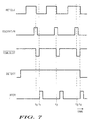
- lock detection circuit 100 may best be understood with the waveform plot of FIG. 7 which illustrate a phase lock condition and a detection of an out-of-lock condition.
- the OSCOUT/N signal and the REFCLK signal are both logic one producing a logic zero at the output of NAND gate 170 and a logic zero at the output of NOR gate 178.
- the TIMESLOT signal of FIG. 7 is high before time to turning on transistor 172 and passing the logic zero to the first input of NOR gate 178.
- Transistor 180 latches the logic zero back to the input of inverter 174.
- TIMESLOT signal When the TIMESLOT signal goes to logic zero, transistor 172 turns off and transistor 184 turns on by inverter 186.
- the zero-going transition of the TIMESLOT signal samples the logic state of the REFCLK signal and the OSCOUT/N signal. If both are logic one, the output of NAND gate 170 is logic zero. Otherwise, the output of NAND gate 170 is logic one.
- the REFCLK signal and the OSCOUT/N signal both transition to logic zero between times t 0 and t 1 of FIG. 7 producing a logic one at the output of NOR gate 178 which passes through transistor 184 and inverters 188 and 190.
- Inverter 194 provides a logic zero at its output.
- Transistor 196 latches the logic one at the input of inverter 188.
- transistor 200 conducts the logic zero from inverter 194 to inverter 202 and provides a logic one DETECT signal.
- the positive-going transition of the TIMESLOT signal again samples the logic state of the REFCLK signal and the OSCOUT/N signal. If both are logic zero and the output of inverter 176 is logic zero, the output of NOR gate 178 is logic one. Otherwise, the output of NOR gate 178 is logic zero.
- the DETECT signal remains at logic one indicating a lock condition for PLL 10.
- the REFCLK signal changes frequency after time t 2 such that PLL 10 is no longer in phase lock.
- the OSCOUT/N signal and the REFCLK signal are both logic one producing a logic zero at the output of NAND gate 170 and a logic zero at the output of NOR gate 178.
- the TIMESLOT signal is high before time t 3 turning on transistor 172 and passing the logic zero to the first input of NOR gate 178.
- Transistor 180 latches the logic zero at the input of inverter 174.
- transistor 172 turns off and transistor 184 turns on by inverter 186, thereby sampling the logic state of the REFCLK signal and the OSCOUT/N signal.
- the OSCOUT/N signal transitions to logic zero between times t 3 and t 4 ; however, REFCLK signal remains at logic one.
- the logic zero output of NOR gate 178 passes through transistor 184 and inverters 188 and 190.
- Transistor 196 latches the logic zero at the input of inverter 188.
- transistor 200 conducts the logic one from inverter 194 to inverter 202 and provides a logic zero DETECT signal indicating a loss of phase lock for PLL 10.
- the positive-going sample detects the REFCLK signal out-of-phase with the OSCOUT/N signal.
- the logic zero DETECT signal shifts into shift register 164 of FIG. 1 at the next SAMPLE CLOCK signal which drives the LOCK signal at output terminal 168 to a logic zero false state.
- the lock detection feature of PLL 10 detects a change of frequency of the REFCLK signal and produces a false LOCK signal.
- the REFCLK and OSCOUT/N signals must both be logic one so that the output of NAND gate 178 is logic zero before the zero-going transition of the TIMESLOT signal. Furthermore, the REFCLK and OSCOUT/N signals must both be logic zero so that the output of NOR gate 118 is logic one by the time of the positive-going transition of the TIMESLOT signal to indicate a phase locked condition for PLL 10.
Landscapes
- Stabilization Of Oscillater, Synchronisation, Frequency Synthesizers (AREA)
Claims (5)
- Programmierbarer Frequenzteiler, der umfaßt:einen Latch-Schaltkreis (60) mit einem ersten und einem zweiten Dateneingang und mit einem Ausgang, wobei der erste Dateneingang eine Programmzahl empfängt und der Ausgang eine ganze Latch-Zahl abgibt,einen Dekrementschaltkreis (62) mit einem Dateneingang, mit einem Takteingang zum Empfangen von einem ersten und einem zweiten Taktsignal und mit einem Ausgang, wobei der Dateneingang mit dem Ausgang des Latch-Schaltkreises gekoppelt ist und der Ausgang mit dem zweiten Eingang des Latch-Schaltkreises gekoppelt ist,einen Vergleicherschaltkreis (64) mit einem ersten und einem zweiten Eingang und mit einem Ausgang, wobei der erste Eingang die ganze Latch-Zahl empfängt und der zweite Eingang eine konstante ganze Zahl empfängt,einen Verzögerungsschaltkreis (68 - 80) mit einem mit dem Ausgang des Vergleicherschaltkreises gekoppelten Eingang, welcher auf das erste und zweite Taktsignal reagiert, um ein erstes Ausgangssignal mit geteilter Frequenz bereitzustellen, wobei der Verzögerungsschaltkreis enthält:(a) einen ersten Transistor (68) mit einem Gate, einem Drain und einer Source, wobei der Drain mit dem Ausgang des Vergleicherschaltkreises gekoppelt ist und das Gate das erste Taktsignal empfängt,(b) einen ersten Inverter (70) mit einem Eingang und einem Ausgang, wobei der Eingang mit der Source des ersten Transistors gekoppelt ist,(c) einen zweiten Transistor (72) mit einem Gate, einem Drain und einer Source, wobei der Drain mit dem Ausgang des ersten Inverters gekoppelt ist und das Gate das zweite Taktsignal empfängt,(d) einen zweiten Inverter (74) mit einem Eingang und einem Ausgang, wobei der Eingang mit der Source des zweiten Transistors gekoppelt ist, und(e) einen dritten Inverter (80) mit einem mit dem Ausgang des zweiten Inverters gekoppelten Eingang,ein erstes UND-Gatter (84) mit einem mit dem Ausgang des zweiten Inverters gekoppelten ersten Eingang, mit einem zum Empfang des ersten Taktsignals gekoppelten zweiten Eingang und mit einem mit einem ersten Ladeeingang des Latch- Schaltkreises gekoppelten Ausgang, wobei ein Signal am Ausgang verursacht, daß die Programmzahl in den Latch-Schaltkreis geladen wird, undein zweites UND-Gatter (86) mit einem mit einem Ausgang des dritten Inverters gekoppelten ersten Eingang, mit einem zum Empfang des ersten Taktsignals gekoppelten zweiten Eingang und mit einem mit einem zweiten Ladeeingang des Latch-Schaltkreises gekoppelten Ausgang.
- Programmierbarer Frequenzteiler nach Anspruch 1, bei dem der Verzögerungsschaltkreis außerdem umfaßt:einen dritten Transistor (108) mit einem Gate, einem Drain und einer Source, wobei der Drain mit dem Ausgang des dritten Inverters gekoppelt ist, das Gate das erste Taktsignal empfängt, undeinen vierten Inverter (110) mit einem Eingang und einem Ausgang, wobei der Eingang mit der Source des dritten Transistors gekoppelt ist und der Ausgang einen Abtasttakt als Ausgangssignal liefert.
- Phasenregelkreis, der umfaßt:ein erstes Mittel (14, 17) zum Vergleichen der Phase eines ersten und eines zweiten digitalen Eingabesignals und zum Erzeugen eines Ausgangssignals, um eine Regelkreisknotenspannung an einem Regelkreisknoten aufzubauen,einen spannungsgesteuerten Oszillator (24) mit einem mit dem Regelkreisknoten gekoppelten Eingang, der ein erstes Oszillatorsignal liefert, das eine Frequenz hat, wie sie von der Regelkreisknotenspannung festgelegt wird,ein zweites Mittel (28), das zum Empfangen des ersten Oszillatorsignals gekoppelt ist und das erste und zweite Taktsignale liefert,einen Latch-Schaltkreis (60) mit einem ersten und einem zweiten Dateneingang, mit einem ersten und einem zweiten Ladeeingang und mit einem Ausgang, wobei der erste Dateneingang eine Programmzahl empfängt, der Ausgang eine Latch-Zahl liefert,einen Dekrementschaltkreis (62) mit einem Eingang, einem ersten und zweiten Takteingang und mit einem Ausgang, wobei der Eingang mit dem Ausgang des Verriegelungsschaltkeises gekoppelt ist, der Ausgang mit dem zweiten Dateneingang des Verriegelungsschaltkreises gekoppelt ist und der erste und zweite Takteingang das erste bzw. das zweite Taktsignal empfängt,einen Vergleicherschaltkreis (64) mit einem ersten und einem zweiten Eingang und mit einem Ausgang, wobei der erste Eingang die Latch-Zahl empfängt, der zweite Eingang eine konstante Zahl empfängt, undeinen Verzögerungsschaltkreis (68 - 80) mit einem mit dem Ausgang des Vergleicherschaltkreises gekoppelten Eingang, der auf das erste und zweite Taktsignal reagiert, um ein zweites Oszillatorsignal mit einer im Vergleich zum ersten Oszillatorsignal verringerten Frequenz zu liefern, wobei der Verzögerungsschaltkreis enthält:einen ersten Transistor (68) mit einem zum Empfang des ersten Taktsignals gekoppelten Gate und mit einem mit dem Ausgang des Vergleicherschaltkreises gekoppelten Drain,einen ersten Inverter (70) mit einem mit der Source des ersten Transistors gekoppelten Eingang,einen zweiten Transistor (72) mit einem zum Empfang des zweiten Taktsignals gekoppelten Gate und mit einem mit einem Ausgang des ersten Inverters gekoppelten Drain,einen zweiten Inverter (74) mit einem mit der Source des ersten Transistors gekoppelten Eingang undeinen dritten Inverter (80) mit einem mit dem Ausgang des zweiten Inverters gekoppelten Eingang,ein erstes UND-Gatter (84) mit einem mit dem Ausgang des zweiten Inverters gekoppelten Eingang und mit einem zum Empfang des ersten Taktsignals gekoppelten zweiten Eingang und mit einem mit dem ersten Ladeeingang des Latch-Schaltkreises gekoppelten Ausgang, undein zweites UND-Gatter (86) mit einem mit einem Ausgang des dritten Inverters gekoppelten ersten Eingang, mit einem zum Empfang des ersten Taktsignals gekoppelten zweiten Eingang und mit einem mit dem zweiten Ladeeingang des Latch-Schaltkreises gekoppelten Ausgang.
- Phasenregelkreis nach Anspruch 3, bei dem der Verzögerungsschaltkreis außerdem umfaßt:einen dritten Transistor (108) mit einem Gate, einem Drain und einer Source, wobei der Drain mit dem Ausgang des dritten Inverters gekoppelt ist, das Gate das erste Taktsignal empfängt, undeinen vierten Inverter (110) mit einem Eingang und mit einem Ausgang, wobei der Eingang mit der Source des dritten Transistors gekoppelt ist und der Ausgang das zweite Oszillatorsignal liefert.
- Verfahren zum Teilen der Frequenz eines Oszillatorsignals, das die Schritte umfaßt:Ableiten eines ersten (XCLK) und eines zweiten (YCLK) Taktsignals vom Oszillatorsignal,Bereitstellen einer Latch-Zahl,Vergleichen der Latch-Zahl mit einer konstanten Zahl (K) und Erzeugen eines FLAG-Signals (FLAG) mit einem ersten Zustand, wenn die Latch-Zahl nicht mit der konstanten Zahl (K) übereinstimmt, und mit einem zweiten Zustand, wenn die Latch-Zahl mit der konstanten Zahl (K) übereinstimmt,Verzögern des FLAG-Signals in Abhängigkeit vom ersten Taktsignal (XCLK) zum Erzeugen eines verzögerten Signals an einem ersten Knoten,Verzögern des verzögerten Signals vom ersten Knoten in Abhängigkeit vom zweiten Taktsignal (YCLK) zum Erzeugen eines verzögerten Signals an einem zweiten Knoten (76),Herabsetzen der Latch-Zahl entsprechend dem ersten und zweiten Taktsignal, wenn das verzögerte Signal am zweiten Knoten (76) einen ersten Zustand hat, und Laden einer Programmzahl (N) als Latch-Zahl in Abhängigkeit vom ersten Taktsignal, wenn das verzögerte Signal am zweiten Knoten (76) einen zweiten Zustand hat, zum Bereitstellen eines zweiten Oszillatorsignals mit einer von der Programmzahl (N) bestimmten Frequenz.
Applications Claiming Priority (2)
| Application Number | Priority Date | Filing Date | Title |
|---|---|---|---|
| US47524 | 1993-04-19 | ||
| US08/047,524 US5359635A (en) | 1993-04-19 | 1993-04-19 | Programmable frequency divider in a phase lock loop |
Publications (2)
| Publication Number | Publication Date |
|---|---|
| EP0625826A1 EP0625826A1 (de) | 1994-11-23 |
| EP0625826B1 true EP0625826B1 (de) | 1999-08-25 |
Family
ID=21949464
Family Applications (1)
| Application Number | Title | Priority Date | Filing Date |
|---|---|---|---|
| EP94104167A Expired - Lifetime EP0625826B1 (de) | 1993-04-19 | 1994-03-17 | Digitaler programmierbarer Frequenzteiler in einem Phasenregelkreis |
Country Status (4)
| Country | Link |
|---|---|
| US (1) | US5359635A (de) |
| EP (1) | EP0625826B1 (de) |
| JP (2) | JP3696899B2 (de) |
| DE (1) | DE69420180T2 (de) |
Families Citing this family (10)
| Publication number | Priority date | Publication date | Assignee | Title |
|---|---|---|---|---|
| JPH07202649A (ja) * | 1993-12-27 | 1995-08-04 | Toshiba Corp | 逓倍回路 |
| US6616254B1 (en) | 1997-06-20 | 2003-09-09 | Itran Communications Ltd. | Code shift keying transmitter for use in a spread spectrum communications system |
| US6009139A (en) * | 1998-06-19 | 1999-12-28 | International Business Machines Corporation | Asynchronously programmable frequency divider circuit with a symmetrical output |
| US6614864B1 (en) | 1999-10-12 | 2003-09-02 | Itran Communications Ltd. | Apparatus for and method of adaptive synchronization in a spread spectrum communications receiver |
| US6798858B1 (en) | 2000-02-04 | 2004-09-28 | International Business Machines Corporation | Lock detector for delay or phase locked loops |
| CN101040238B (zh) * | 2004-08-17 | 2010-05-05 | Nxp股份有限公司 | 混合信号集成电路 |
| CN1331309C (zh) * | 2004-09-30 | 2007-08-08 | 中国科学院微电子研究所 | 一种可任意编程的分频器电路及方法 |
| KR100682830B1 (ko) * | 2005-08-10 | 2007-02-15 | 삼성전자주식회사 | 락 검출기 및 이를 구비하는 지연 동기 루프 |
| CN101087141B (zh) * | 2007-07-10 | 2010-05-19 | 中国人民解放军国防科学技术大学 | 脉冲合成方式的占空比可调n次分频电路 |
| CN105610438B (zh) * | 2015-12-22 | 2019-03-08 | 华为技术有限公司 | 一种除三分频器电路 |
Citations (2)
| Publication number | Priority date | Publication date | Assignee | Title |
|---|---|---|---|---|
| EP0474616A2 (de) * | 1990-09-06 | 1992-03-11 | Ericsson Inc. | Zählschaltung mit zwei Modulen |
| EP0498450A2 (de) * | 1991-02-07 | 1992-08-12 | Nec Corporation | Schaltungsanordnung zum Erzeugen eines seriellen Taktsignals |
Family Cites Families (8)
| Publication number | Priority date | Publication date | Assignee | Title |
|---|---|---|---|---|
| JPS5445558A (en) * | 1977-09-17 | 1979-04-10 | Citizen Watch Co Ltd | Frequency adjusting set for oscillator |
| US4573017A (en) * | 1984-01-03 | 1986-02-25 | Motorola, Inc. | Unitary phase and frequency adjust network for a multiple frequency digital phase locked loop |
| US4882505A (en) * | 1986-03-24 | 1989-11-21 | International Business Machines Corporation | Fully synchronous half-frequency clock generator |
| DE3741423A1 (de) * | 1987-12-08 | 1989-06-22 | Licentia Gmbh | Digitale phaseneinstellung fuer digital generierte signale |
| DE3807875A1 (de) * | 1988-03-10 | 1989-09-21 | Blaupunkt Werke Gmbh | Schaltungsanordnung zum erkennen des auftretens eines vorgebbaren zaehlerstandes |
| US4937846A (en) * | 1988-08-01 | 1990-06-26 | Allied Signal Inc. | Frequency counter-locked-loop apparatus for controlling digitally programmable oscillators |
| JP2561750B2 (ja) * | 1990-10-30 | 1996-12-11 | 三菱電機株式会社 | パルス発生回路 |
| US5155748A (en) * | 1991-04-04 | 1992-10-13 | Zenith Electronics Corporation | Programmable multi-source IR detector |
-
1993
- 1993-04-19 US US08/047,524 patent/US5359635A/en not_active Expired - Lifetime
-
1994
- 1994-03-17 EP EP94104167A patent/EP0625826B1/de not_active Expired - Lifetime
- 1994-03-17 DE DE69420180T patent/DE69420180T2/de not_active Expired - Fee Related
- 1994-04-18 JP JP10174494A patent/JP3696899B2/ja not_active Expired - Fee Related
-
2005
- 2005-02-17 JP JP2005041013A patent/JP2005198339A/ja active Pending
Patent Citations (2)
| Publication number | Priority date | Publication date | Assignee | Title |
|---|---|---|---|---|
| EP0474616A2 (de) * | 1990-09-06 | 1992-03-11 | Ericsson Inc. | Zählschaltung mit zwei Modulen |
| EP0498450A2 (de) * | 1991-02-07 | 1992-08-12 | Nec Corporation | Schaltungsanordnung zum Erzeugen eines seriellen Taktsignals |
Also Published As
| Publication number | Publication date |
|---|---|
| EP0625826A1 (de) | 1994-11-23 |
| US5359635A (en) | 1994-10-25 |
| JP2005198339A (ja) | 2005-07-21 |
| JP3696899B2 (ja) | 2005-09-21 |
| DE69420180T2 (de) | 2000-03-16 |
| JPH0795062A (ja) | 1995-04-07 |
| DE69420180D1 (de) | 1999-09-30 |
Similar Documents
| Publication | Publication Date | Title |
|---|---|---|
| US5278520A (en) | Phase lock detection in a phase lock loop | |
| US5256989A (en) | Lock detection for a phase lock loop | |
| US5495205A (en) | Digital controlled oscillator and method thereof | |
| US5699020A (en) | Phase latched differential charge pump circuit and method | |
| US6011732A (en) | Synchronous clock generator including a compound delay-locked loop | |
| US5940609A (en) | Synchronous clock generator including a false lock detector | |
| US6166572A (en) | Voltage-controlled delay line, direct phase controlled voltage-controlled oscillator, clock/data recovery circuit, and clock/data recovery apparatus | |
| US5389898A (en) | Phase locked loop having plural selectable voltage controlled oscillators | |
| JP2795323B2 (ja) | 位相差検出回路 | |
| US6496554B1 (en) | Phase lock detection circuit for phase-locked loop circuit | |
| US7495488B2 (en) | Phase-locked loop circuit, delay-locked loop circuit and method of tuning output frequencies of the same | |
| EP0614275B1 (de) | Vorrichtung und Verfahren mit Schieberegistern zur Erzeugung einer Vorspannung für einen VCO in einer PLL-Schaltung | |
| US6628171B1 (en) | Method, architecture and circuit for controlling and/or operating an oscillator | |
| JP2005198339A (ja) | 位相ロック・ループにおけるプログラム可能周波数分周器 | |
| US5838205A (en) | Variable-speed phase-locked loop system with on-the-fly switching and method therefor | |
| US5008629A (en) | Frequency synthesizer | |
| US5974105A (en) | High frequency all digital phase-locked loop | |
| EP2359469B1 (de) | Phasenfrequenzdetektor | |
| KR20030017623A (ko) | 반도체 집적회로 | |
| US6614317B2 (en) | Variable lock window for a phase locked loop | |
| KR100234729B1 (ko) | 디지탈 디엘엘 회로 | |
| US6538517B2 (en) | Frequency phase detector for differentiating frequencies having small phase differences | |
| US20070035338A1 (en) | Symmetric D flip-flop and phase frequency detector including the same | |
| JPH09214333A (ja) | 半導体集積回路 | |
| US6430244B1 (en) | Digital phase-locked loop apparatus with enhanced phase error compensating circuit |
Legal Events
| Date | Code | Title | Description |
|---|---|---|---|
| PUAI | Public reference made under article 153(3) epc to a published international application that has entered the european phase |
Free format text: ORIGINAL CODE: 0009012 |
|
| AK | Designated contracting states |
Kind code of ref document: A1 Designated state(s): DE FR GB |
|
| 17P | Request for examination filed |
Effective date: 19950523 |
|
| 17Q | First examination report despatched |
Effective date: 19970414 |
|
| GRAG | Despatch of communication of intention to grant |
Free format text: ORIGINAL CODE: EPIDOS AGRA |
|
| GRAG | Despatch of communication of intention to grant |
Free format text: ORIGINAL CODE: EPIDOS AGRA |
|
| GRAH | Despatch of communication of intention to grant a patent |
Free format text: ORIGINAL CODE: EPIDOS IGRA |
|
| GRAH | Despatch of communication of intention to grant a patent |
Free format text: ORIGINAL CODE: EPIDOS IGRA |
|
| GRAA | (expected) grant |
Free format text: ORIGINAL CODE: 0009210 |
|
| AK | Designated contracting states |
Kind code of ref document: B1 Designated state(s): DE FR GB |
|
| ET | Fr: translation filed | ||
| REF | Corresponds to: |
Ref document number: 69420180 Country of ref document: DE Date of ref document: 19990930 |
|
| PLBE | No opposition filed within time limit |
Free format text: ORIGINAL CODE: 0009261 |
|
| STAA | Information on the status of an ep patent application or granted ep patent |
Free format text: STATUS: NO OPPOSITION FILED WITHIN TIME LIMIT |
|
| 26N | No opposition filed | ||
| REG | Reference to a national code |
Ref country code: GB Ref legal event code: IF02 |
|
| PGFP | Annual fee paid to national office [announced via postgrant information from national office to epo] |
Ref country code: GB Payment date: 20020205 Year of fee payment: 9 |
|
| PGFP | Annual fee paid to national office [announced via postgrant information from national office to epo] |
Ref country code: FR Payment date: 20020228 Year of fee payment: 9 |
|
| PGFP | Annual fee paid to national office [announced via postgrant information from national office to epo] |
Ref country code: DE Payment date: 20020327 Year of fee payment: 9 |
|
| PG25 | Lapsed in a contracting state [announced via postgrant information from national office to epo] |
Ref country code: GB Free format text: LAPSE BECAUSE OF NON-PAYMENT OF DUE FEES Effective date: 20030317 |
|
| PG25 | Lapsed in a contracting state [announced via postgrant information from national office to epo] |
Ref country code: DE Free format text: LAPSE BECAUSE OF NON-PAYMENT OF DUE FEES Effective date: 20031001 |
|
| GBPC | Gb: european patent ceased through non-payment of renewal fee |
Effective date: 20030317 |
|
| PG25 | Lapsed in a contracting state [announced via postgrant information from national office to epo] |
Ref country code: FR Free format text: LAPSE BECAUSE OF NON-PAYMENT OF DUE FEES Effective date: 20031127 |
|
| REG | Reference to a national code |
Ref country code: FR Ref legal event code: ST |
|
| P01 | Opt-out of the competence of the unified patent court (upc) registered |
Effective date: 20230520 |