EP0623934A2 - Speicheranordnungprogrammiergerät - Google Patents
Speicheranordnungprogrammiergerät Download PDFInfo
- Publication number
- EP0623934A2 EP0623934A2 EP94200915A EP94200915A EP0623934A2 EP 0623934 A2 EP0623934 A2 EP 0623934A2 EP 94200915 A EP94200915 A EP 94200915A EP 94200915 A EP94200915 A EP 94200915A EP 0623934 A2 EP0623934 A2 EP 0623934A2
- Authority
- EP
- European Patent Office
- Prior art keywords
- programming
- ramp
- signal
- line
- capacitor
- Prior art date
- Legal status (The legal status is an assumption and is not a legal conclusion. Google has not performed a legal analysis and makes no representation as to the accuracy of the status listed.)
- Ceased
Links
- 239000003990 capacitor Substances 0.000 claims abstract description 31
- 230000004044 response Effects 0.000 claims abstract description 9
- 230000001276 controlling effect Effects 0.000 claims abstract description 6
- 230000000630 rising effect Effects 0.000 claims abstract description 5
- 230000001105 regulatory effect Effects 0.000 claims abstract description 4
- 230000008878 coupling Effects 0.000 claims description 6
- 238000010168 coupling process Methods 0.000 claims description 6
- 238000005859 coupling reaction Methods 0.000 claims description 6
- 238000010586 diagram Methods 0.000 description 5
- 230000005540 biological transmission Effects 0.000 description 3
- 230000009977 dual effect Effects 0.000 description 1
- 230000006870 function Effects 0.000 description 1
- 230000003071 parasitic effect Effects 0.000 description 1
- 239000000758 substrate Substances 0.000 description 1
Images
Classifications
-
- G—PHYSICS
- G11—INFORMATION STORAGE
- G11C—STATIC STORES
- G11C16/00—Erasable programmable read-only memories
- G11C16/02—Erasable programmable read-only memories electrically programmable
- G11C16/06—Auxiliary circuits, e.g. for writing into memory
- G11C16/10—Programming or data input circuits
- G11C16/12—Programming voltage switching circuits
-
- G—PHYSICS
- G11—INFORMATION STORAGE
- G11C—STATIC STORES
- G11C16/00—Erasable programmable read-only memories
- G11C16/02—Erasable programmable read-only memories electrically programmable
- G11C16/06—Auxiliary circuits, e.g. for writing into memory
- G11C16/10—Programming or data input circuits
Definitions
- the present invention relates to programming apparatus for a memory device, for example an EEPROM.
- memory circuits such as EEPROMs are operated at a fixed voltage, for example 5 volts, provided by a regulated voltage supply.
- the EEPROM circuits are characteristically programmable in response to a high level programming signal.
- the programming signals are generally provided at a voltage level higher than the normal operating voltage of the EEPROM, for example in the order of 14 volts.
- the present invention seeks to provide improved programming apparatus.
- the invention can provide a ramp control circuit for use in programming a memory device which controls the ramp-up time of the programming signal to the device.
- the circuit may control the ramp-down time of the programming signal so as to prevent forward biasing of junctions of the memory device.
- the programming signal ramp-up and ramp-down times are independent of load applied to the programming signal source.
- a low resistance path may be provided from a programming signal source to a memory device so as to minimise the voltage drop between the signal source and the device.
- a preferred embodiment comprises a charge pump controlling ramp-up of a gate signal in response to a programming signal, a transistor coupling the programming signal input to a programming output responsive to the charge pump gate signal, a ramp control circuit coupled to the programming output line comprising means for limiting the rate at which a signal on the programming output line may be ramped-up and a pull-down circuit for sensing a falling edge of the programming signal and providing controlled ramp-down of the programming output signal in a manner to avoid forward biasing of junctions of the memory device.
- This invention can be used with a typical EEPROM characterised by (i) normal operation at a fixed voltage, for example 5 volts, and (ii) programming operation in response to a programming signal at a voltage higher than the normal operating voltage, that is a programming signal of the order of 14 volts.
- EEPROMs of this nature are well known to those skilled in the art.
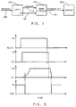
- the EEPROM programmer shown includes a program signal line 208 which provides a programming signal of the order of 14 volts to logic circuitry 202.
- Logic circuitry 202 responsively provides the programming signal (SCLK) on line 14 and an enable signal (EN) on line 64 to the ramp circuit 204.
- Logic circuitry 202 provides the signals SCLK and EN on lines 14 and 64 according to the timing diagram shown in Figure 3 (discussed below), by sensing the rising edge of the programming signal and by responsively providing the rising edge of the signal EN with a slight delay.
- logic circuitry 202 senses the falling edge of the programming signal and causes signal EN to fall after a slight delay, so that signal EN trails the programming signal with a slight delay.
- Those skilled in the art can easily implement logic circuitry 202 to perform these described functions and circuits for providing the signals SCLK and EN as described in Figure 3.
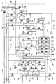
- the circuit shown comprises three main operational sections, charge pump 20 for controlling ramp-up of line 50, which is the gate input of transistor 52, ramping control circuit 58, which controls the ramp-up time of the programming signal output line 130 and pull-down circuit 92, which controls the ramp-down time of programming output line 130.
- charge pump 20 receives a clock signal (for example 500 kHz) on line 21 through inverters 22 and 24.
- Inverters 22 and 24 responsively provide first and second clock signals in opposite phase to transmission gates 26 and 30.
- Transmission gates 26 and 30 are switched "active" by a high signal on enable line 64, which is coupled directly to the n-channel devices and via inverter 28 to the p-channel devices.
- capacitors 34 and 36 alternately provide charge currents to transistors 42 and 44, alternately switching transistors 42 and 44 on and off.
- Transistor 40 is connected in series with transistors 42 and 44 and capacitor 62 (a dual plate on-chip capacitor of, for example, 2 pF) between line 14 and ground. Transistor 40, held active by the enable signal on line 64, provides a current path from line 14 to the series circuit of transistors 42 and 44 and capacitor 62. As transistors 42 and 44 alternately switch on and off, capacitor 62 charges. As the charging action of charge pump 20 charges capacitor 62, line 50 rises to a voltage level between 3 and 5 volts above the level of the programming signal SCLK on programming input line 14.
- transistor 52 is gated on, coupling the programming signal from the programming input line 44 to the programming output line 130, which provides the programming output signal to EEPROM 206 ( Figure 1).
- transistor 90 passes current at a level set by the voltage bias line 10 and by the channel size of transistor 90.
- line 10 is set at approximately 3.5 volts, which is at least one p-channel threshold below the voltage supply rail providing the voltage Vdd.
- Transistor 90 mirrors the current through transistors 68-86, which mirror the current to transistor 56 to pull line 55 low, maintaining transistor 48 off.
- Capacitor 54 tries to pull line 55 high from the signal coupled to line 130 through transistor 52.
- the charging of capacitor 54 is controlled by the amount of current allowed through transistor 56 which, in turn, is controlled by the current mirror transistors 68-86. This charging rate of capacitor 54 controls the ramp-up time of the programming output signal on line 130 so that the ramp-up time period is about 200 microseconds.
- the charging time of 200 microseconds is achieved with the capacitance 2 pF for capacitor 54, gate widths and lengths of 2 and 3 micrometres, respectively, for transistors 56 and 68-86, and a gate width and length of 9 and 10 micrometres, respectively, for transistor 90.
- transistor 52 is fully on and provides a low impedance path between input programming signal line 14 and output programming signal line 130.
- programming line 14 is high, normally transistors 98, 100 and 102 maintain line 89 low and transistor 88 off.
- transistor 100 When the falling edge of the programming signal on line 14 is sensed via capacitor 94, transistor 100 quickly turns on bringing line 89 up to the supply voltage level and turning on transistor 88, which pulls line 50 to ground, quickly shutting off transistor 52.
- Transistors 106 and 110 mirror ten percent of the current from transistors 68-86 and, in conjunction with transistors 104 and 108, set the bias voltage for transistors 100 and 102 to a point where transistor 100 is barely turned off.
- capacitor 126 (of 1 pF) discharges through the circuit of transistors 122, 124 and 128, providing a fast and controlled ramp-down of the programming signal on line 130, with a ramp-down time of approximately 15-20 microseconds.
- Gate sizes for transistors 122 and 128 are 7.5 by 10 micrometres (width by length) and for transistor 124 is 5 by 2 micrometres (width by length).
- Inverter 131 is coupled to line 130 and inverts the signal on line 130 so that, as line 130 goes low in response to line 14 going low and achieves a level about one n-threshold above ground, inverter 131 provides a high output signal on line 12.
- inverter 96 provides a low signal to transistor 114 turning off transistor 114.
- transistor 114 is off, the gate of transistor 120 goes high, maintaining line 130 at ground.
- the circuit inhibits transfer of the programming signal to the programming output line 130.
- Transistor 16 brings line 61 high, disabling the circuit, if no VDD is present, as follows.
- line 61 is high, which also occurs when enable line 64 goes low, transistor 46 is turned on pulling line 50 to ground, maintaining transistor 52 off so that no programming signals can be transferred from line 14 to line 130.
- inverter 109 inverts the signal on line 61 to provide a low signal to transistors 118 and 124 maintaining transistors 118 and 124 off.
- transistor 128 When transistor 124 is off, transistor 128 is biased positive by transistor 122 and provides a discharge path from line 130 to ground via the source drain circuit of transistor 128. Capacitor 126 affects the rate of discharge of line 130. Also, when transistor 118 is off, the gate of transistor 120 is pulled high by transistor 112 and/or transistor 116, turning on transistor 120, which maintains line 130 low.
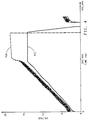
- the timing diagram shows the circuit signals SCLK on line 14, EN on line 64, HV on line 130 and HVB on line 12.
- the programming signal SCLK goes high and logic circuit 202 brings the enable signal EN on line 64 high immediately following rising edge of SCLK.
- EN goes high
- the signal HV on line 130 responsively ramps up.
- logic circuitry (202, Figure 1) provides immediately thereafter a drop of the enable signal EN as shown which causes, as explained above, transistor 128 to be gated on, allowing line 130 to ramp-down via discharge of capacitor 126 through transistor 128.
- signal HVB which is the output of inverter 131, goes high as shown.
- Figure 4 illustrates as trace 152 the ramping-up and down of the signal HV on line 130 and, as trace 150, the ramping-up and down of the signal on line 50 driving the gate of transistor 52.
- the circuitry described above prevents forward biasing of junctions in EEPROM circuitry by controlling the ramp-down time to be a minimum of 10 microseconds. If the ramp-down time of the programming signal on line 130 is too fast, junctions in EEPROM circuitry may be forward biased causing current to be dumped into the substrate and unwanted parasitic activity.
Landscapes
- Read Only Memory (AREA)
Applications Claiming Priority (2)
| Application Number | Priority Date | Filing Date | Title |
|---|---|---|---|
| US08/055,593 US5408133A (en) | 1993-05-03 | 1993-05-03 | Ramp control circuit |
| US55593 | 1993-05-03 |
Publications (2)
| Publication Number | Publication Date |
|---|---|
| EP0623934A2 true EP0623934A2 (de) | 1994-11-09 |
| EP0623934A3 EP0623934A3 (de) | 1995-04-26 |
Family
ID=21998896
Family Applications (1)
| Application Number | Title | Priority Date | Filing Date |
|---|---|---|---|
| EP94200915A Ceased EP0623934A3 (de) | 1993-05-03 | 1994-04-05 | Speicheranordnungprogrammiergerät. |
Country Status (3)
| Country | Link |
|---|---|
| US (1) | US5408133A (de) |
| EP (1) | EP0623934A3 (de) |
| JP (1) | JPH076591A (de) |
Families Citing this family (6)
| Publication number | Priority date | Publication date | Assignee | Title |
|---|---|---|---|---|
| FR2768274B1 (fr) * | 1997-09-10 | 1999-11-05 | Sgs Thomson Microelectronics | Circuit de generation d'une haute tension de programmation ou d'effacement d'une memoire |
| FR2770325B1 (fr) * | 1997-10-29 | 2001-10-05 | Sgs Thomson Microelectronics | Circuit generateur de tension pour programmer ou effacer une memoire qui utilise des transistors a grille flottante |
| KR100453854B1 (ko) * | 2001-09-07 | 2004-10-20 | 삼성전자주식회사 | 향상된 프로그램 방지 특성을 갖는 불휘발성 반도체메모리 장치 및 그것의 프로그램 방법 |
| US6603335B1 (en) | 2002-06-11 | 2003-08-05 | Sige Semiconductor Inc. | Ramp circuit to reduce spectral regrowth of power amplifiers |
| US6980047B1 (en) | 2002-06-20 | 2005-12-27 | Taiwan Semiconductor Manufacturing Company | Low power high voltage ramp-up control circuit |
| US7630250B2 (en) * | 2007-10-16 | 2009-12-08 | Spansion Llc | Controlled ramp rates for metal bitlines during write operations from high voltage driver for memory applications |
Family Cites Families (16)
| Publication number | Priority date | Publication date | Assignee | Title |
|---|---|---|---|---|
| JPS498446B1 (de) * | 1970-05-07 | 1974-02-26 | ||
| US3916224A (en) * | 1973-08-02 | 1975-10-28 | Ibm | Transistor switching regulator control utilizing charging of bootstrap circuit to provide ramp-up |
| US4488060A (en) * | 1979-01-24 | 1984-12-11 | Xicor, Inc. | High voltage ramp rate control systems |
| US4516036A (en) * | 1982-11-23 | 1985-05-07 | Rca Corporation | Linear ramp voltage generator circuit |
| GB2146502B (en) * | 1983-08-31 | 1987-07-01 | Nat Semiconductor Corp | Internal high voltage (vpp) rise control circuit |
| NL8400225A (nl) * | 1984-01-25 | 1985-08-16 | Philips Nv | Schakeling voor het opwekken van de programmeerspanning van een uitwisbaar leesgeheugen. |
| JPS6148197A (ja) * | 1984-08-13 | 1986-03-08 | Fujitsu Ltd | チヤ−ジアツプ回路 |
| US4859955A (en) * | 1985-11-06 | 1989-08-22 | The Grass Valley Group, Inc. | Apparatus for smoothing an abrupt change in signal level |
| US4855622A (en) * | 1987-12-18 | 1989-08-08 | North American Philips Corporation, Signetics Division | TTL compatible switching circuit having controlled ramp output |
| US4823317A (en) * | 1988-01-20 | 1989-04-18 | Ict International Cmos Technolgy, Inc. | EEPROM programming switch |
| IT1221246B (it) * | 1988-02-04 | 1990-06-27 | Sgs Thomson Microelectronics | Alimentatore con tensione di uscita sviluppata gradualmente all' atto dell' accensione |
| US4888498A (en) * | 1988-03-24 | 1989-12-19 | Texas Instruments Incorporated | Integrated-circuit power-up pulse generator circuit |
| US4942341A (en) * | 1988-06-20 | 1990-07-17 | Sanyo Electric Co., Ltd. | Vertical ramp generator |
| US5315547A (en) * | 1988-07-11 | 1994-05-24 | Hitachi, Ltd. | Nonvolatile semiconductor memory device with selective tow erasure |
| JP2694205B2 (ja) * | 1988-07-11 | 1997-12-24 | 株式会社日立製作所 | 不揮発性半導体記憶装置 |
| US5241494A (en) * | 1990-09-26 | 1993-08-31 | Information Storage Devices | Integrated circuit system for analog signal recording and playback |
-
1993
- 1993-05-03 US US08/055,593 patent/US5408133A/en not_active Expired - Fee Related
-
1994
- 1994-04-05 EP EP94200915A patent/EP0623934A3/de not_active Ceased
- 1994-05-02 JP JP9320494A patent/JPH076591A/ja active Pending
Also Published As
| Publication number | Publication date |
|---|---|
| EP0623934A3 (de) | 1995-04-26 |
| JPH076591A (ja) | 1995-01-10 |
| US5408133A (en) | 1995-04-18 |
Similar Documents
| Publication | Publication Date | Title |
|---|---|---|
| US5646550A (en) | High reliability output buffer for multiple voltage system | |
| US6466063B2 (en) | Push-pull output buffer with gate voltage feedback loop | |
| KR900004196B1 (ko) | 전압수준 감지 전력복귀(power-up reset)회로 | |
| US6281730B1 (en) | Controlled slew rate driver | |
| EP0269185B1 (de) | Schalteinrichtung mit dynamischer Hysterese | |
| EP0700160A2 (de) | Einschalt-Rücksetzschaltung | |
| US20210336611A1 (en) | Area efficient slew-rate controlled driver | |
| US5687122A (en) | Data output buffer | |
| EP0388918B1 (de) | Integrierte Halbleiterschaltung mit einer Substratspannungsdetektorschaltung | |
| EP0623934A2 (de) | Speicheranordnungprogrammiergerät | |
| JPH04167298A (ja) | センス増幅器および出力遷移を速くする方法 | |
| US5489859A (en) | CMOS output circuit with high speed high impedance mode | |
| KR0157885B1 (ko) | 전원 공급 감지 회로 | |
| US6097179A (en) | Temperature compensating compact voltage regulator for integrated circuit device | |
| US4208594A (en) | Power monitor for use in starting and stopping a digital electronic system | |
| EP0580748B1 (de) | Schaltung zur spannungsmessung bei geringer leistung | |
| US5903180A (en) | Voltage tolerant bus hold latch | |
| EP0328168B1 (de) | Push-pull-Ausgangsschaltung, ohne Belastung durch hochenergetische Träger | |
| EP0678800A2 (de) | Datenausgangtreiberschaltung mit Hochziehbetriebanordnung | |
| US5946204A (en) | Voltage booster with reduced Vpp current and self-timed control loop without pulse generator | |
| US20020180495A1 (en) | CMOS output circuit | |
| EP1066685B1 (de) | Verbesserte einschaltrücksetzschaltung | |
| US5796289A (en) | Pass transistor capacitive coupling control circuit | |
| JP3120303B2 (ja) | パワーmos制御回路 | |
| EP4376299A1 (de) | Steuerschaltung für einen ausgangstreiber mit einer anstiegsgeschwindigkeitssteuerschaltung und ausgangstreiber damit |
Legal Events
| Date | Code | Title | Description |
|---|---|---|---|
| PUAI | Public reference made under article 153(3) epc to a published international application that has entered the european phase |
Free format text: ORIGINAL CODE: 0009012 |
|
| AK | Designated contracting states |
Kind code of ref document: A2 Designated state(s): DE FR IT |
|
| PUAL | Search report despatched |
Free format text: ORIGINAL CODE: 0009013 |
|
| AK | Designated contracting states |
Kind code of ref document: A3 Designated state(s): DE FR IT |
|
| 17P | Request for examination filed |
Effective date: 19951026 |
|
| GRAG | Despatch of communication of intention to grant |
Free format text: ORIGINAL CODE: EPIDOS AGRA |
|
| 17Q | First examination report despatched |
Effective date: 19980109 |
|
| STAA | Information on the status of an ep patent application or granted ep patent |
Free format text: STATUS: THE APPLICATION HAS BEEN REFUSED |
|
| 18R | Application refused |
Effective date: 19980702 |