EP0620584B1 - Apparatus and method for providing consistent, non-jamming registration of notched semiconductor wafers - Google Patents
Apparatus and method for providing consistent, non-jamming registration of notched semiconductor wafers Download PDFInfo
- Publication number
- EP0620584B1 EP0620584B1 EP94105574A EP94105574A EP0620584B1 EP 0620584 B1 EP0620584 B1 EP 0620584B1 EP 94105574 A EP94105574 A EP 94105574A EP 94105574 A EP94105574 A EP 94105574A EP 0620584 B1 EP0620584 B1 EP 0620584B1
- Authority
- EP
- European Patent Office
- Prior art keywords
- semiconductor wafer
- wafer
- registration
- roller
- notched
- Prior art date
- Legal status (The legal status is an assumption and is not a legal conclusion. Google has not performed a legal analysis and makes no representation as to the accuracy of the status listed.)
- Expired - Lifetime
Links
Images

Classifications
-
- H10P72/57—
Definitions
- the present invention relates to the registration of semiconductor wafers undergoing multiple sequential processes, such as a metrology step followed by a thinning and/or etching processes and, in particular, relates to an apparatus that provides consistent, non-jamming registration of notched semiconductor wafers in order to correlate the registration of the semiconductor wafers throughout the multiple sequential processes.
- US-A-4 820 930 discloses a positioning device for positioning a mask having formed thereon a pattern to be transferred onto a semiconductor wafer.
- the positioning device positions the mask so that a center of the mask is brought into alignment with a center of rotation of a holder for holding the mask.
- the positioning device includes a plurality of engaging pins to be engaged by the periphery of the marks, each engaging pin being movable in a direction towared the center of rotation of the mask holder. Movement of each of the engaging pins is controlled independently from the others, whereby the mask can be positioned irrespective of its size and/or shape.
- the process of measuring the thickness of an outer material layer of a semiconductor wafer is known as wafer surface metrology.
- a semiconductor wafer is mechanically registered to the stage of a thickness measuring instrument.
- This instrument generates a map that indicates the thickness of an outer material layer of the wafer over an entire surface of the wafer.
- the outer layer thickness map generated from this metrology process is often used in other processes that thin or etch the material of the outer layer of the wafer to a desired thickness or in a desired location, respectively.
- These outer layer thinning and etching processes both include some type of tool that is directed onto the surface of the wafer.
- This tool must be properly positioned along the wafer surface to ensure that the thinning or etching process is performed at the correct location on the wafer surface. To ensure this proper wafer registration, an accurate correlation between the outer layer thickness map and the position of the wafer with respect to the thinning or etching tool is required.
- a current approach for correlating an outer layer thickness map with the position of the wafer in a thinning or etching instrument begins by marking the wafer with a set of alignment fiducials during the metrology process. The wafer is then placed on a larger diameter wafer which serves as a surround. The surround is made of the same material as the wafer undergoing work to maintain a consistent reaction in the thinning or etching process along the wafer edge. The flat of the fiducialized wafer is abutted to a flat registration surface of like wafer material that is taped to the surface of the surround, thereby registering the wafer in one direction.
- the wafer metrology fiducials are then visually aligned with a corresponding set of scribe marks on an aluminum holding plate, or platen, of the instrument. Once aligned, two additional registration surfaces of like wafer material are abutted against the wafer and taped to the surround to maintain the wafer position. The surround is then taped to the platen so that the thinning or etching process may begin.
- An apparatus for achieving such a registration of semiconductor wafers having flats is disclosed in US-A-5 180 150.
- the above-described correlated registration procedure can be time consuming and prone to human error. Furthermore, the above-described procedure does not allow for the correlated registration of notched semiconductor wafers. It is therefore desirable to provide a correlated registration apparatus and procedure that is less time consuming and less prone to human error than the above-described procedure, and that allows correlated registration of notched semiconductor wafers.
- Such a desirable correlation registration procedure is achievable with an apparatus, described more thoroughly hereinafter in the detailed description, that is presently used to provide consistent registration of notched semiconductor wafers in metrology and thinning and etching instruments.
- a disadvantage of this presently used apparatus is that jamming can occur due to friction between the surfaces of the wafer to be registered and the registration surfaces of the apparatus. Thus, it is further desirable to prevent such jamming in this presently used apparatus.
- an apparatus for providing registration of semiconductor wafers undergoing process work in a plurality of process instruments, wherein each said semiconductor wafer undergoing work has a notch formed along a portion of its circumference.
- This known apparatus comprises means for supporting a notched semiconductor wafer to be registered, means for providing registration that accommodates the notch of the semiconductor wafer in the form of a pin which is slidably mounted on the support means, and first and second means for providing a registration that movably accommodates a first and a second point along the circumference of the notched semiconductor wafer in the form of rollers whose axes are slidably mounted on the support means.
- the present invention as defined in claim 1 contemplates an apparatus that provides consistent registration of notched semiconductor wafers and provides correlation between thinning and etching processes and metrology process data.
- Such an apparatus is comprised of a metal mounting plate upon which a notched wafer undergoing work lays flat.
- the wafer is partially registered to the metal plate by two rollers that are fixedly mounted to the plate.
- the first of these fixedly mounted rollers is positioned on the metal plate such that, when the wafer is properly registered, both walls of the wafer notch are abutted against this roller.
- the second of these fixedly mounted rollers is positioned on the metal plate such that the wafer, when properly registered, is abutted against this roller at a point on the wafer approximately -120° from the wafer notch.
- a third, adjustable roller that is fixedly mounted on a moveable metal bracket which allows the roller to move in an approximately radial direction with respect to the wafer.
- This third, adjustable roller applies a force against the wafer, at a point on the wafer approximately 120° from the wafer notch, by way of an external force applied to the moveable metal bracket. This force, coupled with the rolling capability of the rollers, ensures that an initially improperly registered wafer will be rotated into the proper registration position.
- the rollers due to the fact that the rollers, by virtue of having rolling element bearings, generally exhibit only a slight amount of friction, or a rolling friction, the effective coefficient of friction between the rollers and the wafer is significantly less than a critical value in the effective coefficient of friction above which wafer jamming occurs. Thus, the wafer will be properly registered without jamming.
- the rollers and associated mounting plate of the present invention are not subject to this same material constraint.
- this constraint is required in the prior art so that consistent thinning and etching processes are maintained along the wafer edge.
- this material constraint does fulfill the object of maintaining consistent processes, a undesirable result of increased material replacement occurs since the thinning and etching processes depreciatively affect the registration and surround materials.
- the material constraint and resulting material replacement problems of the prior art are overcome in the present invention by shielding the rollers and the associated mounting plate from the depreciative affects of the thinning and etching processes.
- the materials used in the present invention apparatus can be selected with practical considerations such a cost and reliability in mind, instead of impractical and costly material constraints.
- the present invention apparatus described above can be used in thinning, etching, and metrology processes, among others, and provides consistent non-jamming registration of notched semiconductor wafers undergoing process work regardless of diameter variations among processed wafers. Furthermore, the use of this apparatus can decrease the registration time associated with the tedious visual alignment procedures of the prior art, while minimizing the potential for human error.
- the primary object of the present invention is to provide an apparatus that provides consistent, non-jamming registration of notched semiconductor wafers.
- Another object of the present invention is to provide an apparatus that can accurately correlate metrology process data to wafer registration in thinning and etching process instruments.
- Another object of the present invention is to provide an apparatus that decreases wafer registration time as compared to prior art registration procedures.
- Figure 1 is a plan view of a prior art notched semiconductor wafer registration apparatus that is experiencing wafer jamming.
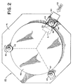
- Figure 2 is plan view of a notched semiconductor wafer registration apparatus embodying the principles of the present invention wherein rollers are used to consistently register notched semiconductor wafers.
- FIG. 1 there is shown a prior art notched semiconductor wafer registration apparatus 10 , the use of which can result in wafer-jamming.
- This prior art apparatus 10 maintains a surround 12 upon which two registration surfaces 14 , 15 and two guides 24 are fixedly mounted.
- the first 14 of the two 14,15 fixedly mounted registration surfaces is used for registering a notch 18 of a wafer 16 .
- the second 15 of the two 14, 15 fixedly mounted registration surfaces is positioned to register a point 20 on the wafer 16 approximately -120° from the wafer notch 18 .
- a third, adjustable registration surface 22 is placed between the two fixedly mounted guides 24 .
- a force 26 is applied to this third, adjustable registration surface 22 , and hence to the wafer 16 .
- This force 26 tends to rotate the wafer 16 about a virtual pivot 28 until contact is made with all of the registration surfaces 14,15,22 .
- friction at the points of contact between the wafer 16 and the registration surfaces 14,15,22 tends to impede this necessary rotation.
- a critical value in the effective coefficient of friction between the wafer 16 and the registration surfaces 14,15,22 exists above which the necessary rotation does not occur regardless of the magnitude of the applied force 26 . This results in a friction jam that causes the wafer 16 to be improperly registered as shown.
- FIG. 2 there is shown a notched semiconductor wafer registration apparatus 40 according to the present invention that overcomes the previously mentioned friction-jamming problems of the prior art.
- This apparatus 40 maintains an aluminum plate 41 upon which two rollers 42,43 , and two guides 44 are fixedly mounted.
- the aluminum plate 41 also provides an area upon which a semiconductor wafer 46 can be laid flat.
- the first 42 of the two 42,43 fixedly mounted rollers is positioned on the plate 41 such that, when the wafer 46 is properly registered, both walls of the wafer notch 45 are abutted against this roller 42 .
- the second 43 fixedly mounted roller is positioned on the plate 41 such that the wafer 46 , when properly registered, is abuttted against this roller 43 at a point 47 on the wafer 46 approximately -120° from the wafer notch 45 .
- a third, adjustable roller 48 is fixedly mounted to a sliding aluminum bracket 50 that is positioned between the two guides 44 and within a radial groove 51 that has been fabricated or milled into the aluminum plate 41 .
- the purpose of the two guides 44 and the radial groove 51 is to restrict the sliding aluminum bracket 50 , and hence the third roller 48 , to an approximately radial movement with respect to the wafer 46 .
- the sliding aluminum bracket 50 can be replaced b a pivot arm adapted to pivot about a pivot pin mounted to the plate 41 .
- a external force 52 is applied to the sliding aluminum bracket 50 .
- This externally applied force 52 results in the third roller 48 applying a similar force against the wafer 46 at a point 53 on the wafer approximately 120° from the wafer notch 45 .
- This resulting force coupled with the rolling capability of the rollers 42, 43, 48 , ensures that an improperly registered wafer will be rotated into the proper registration position, a shown.
- the rollers 42, 43, 48 by virtue of having rolling element bearings, generally exhibit only a slight amount of friction, or a rolling friction, the effective coefficient of friction between the rollers 42 , 43, 48 and the wafer 46 is significantly less than the critical value in the effective coefficient of friction above which wafer jamming occurs.
- the wafer 46 will be properly registered without jamming.
- proper registration will only occur when the wafer 46 is originally positioned on the plate 41 in a manner that will allow such registration; i.e. the wafer notch 45 must be in sufficiently close proximity to the first roller 42 .
- the present state of the art in wafer handling systems is such that this original positioning condition should be easily achieved.
Landscapes
- Container, Conveyance, Adherence, Positioning, Of Wafer (AREA)
- Jigs For Machine Tools (AREA)
Applications Claiming Priority (2)
| Application Number | Priority Date | Filing Date | Title |
|---|---|---|---|
| US4605393A | 1993-04-12 | 1993-04-12 | |
| US46053 | 1993-04-12 |
Publications (2)
| Publication Number | Publication Date |
|---|---|
| EP0620584A1 EP0620584A1 (en) | 1994-10-19 |
| EP0620584B1 true EP0620584B1 (en) | 1997-01-02 |
Family
ID=21941330
Family Applications (1)
| Application Number | Title | Priority Date | Filing Date |
|---|---|---|---|
| EP94105574A Expired - Lifetime EP0620584B1 (en) | 1993-04-12 | 1994-04-11 | Apparatus and method for providing consistent, non-jamming registration of notched semiconductor wafers |
Country Status (5)
| Country | Link |
|---|---|
| EP (1) | EP0620584B1 (OSRAM) |
| JP (1) | JPH0758186A (OSRAM) |
| DE (1) | DE69401295T2 (OSRAM) |
| IL (1) | IL109193A0 (OSRAM) |
| TW (1) | TW244392B (OSRAM) |
Families Citing this family (8)
| Publication number | Priority date | Publication date | Assignee | Title |
|---|---|---|---|---|
| DE19729714C2 (de) * | 1997-07-11 | 2002-11-07 | Brooks Automation Gmbh | Vorrichtung und Verfahren zur Orientierung von kreisförmigen Substraten |
| KR100475732B1 (ko) * | 1997-09-13 | 2005-07-05 | 삼성전자주식회사 | 포토설비의웨이퍼얼라인장치 |
| FR2778496B1 (fr) | 1998-05-05 | 2002-04-19 | Recif Sa | Procede et dispositif de changement de position d'une plaque de semi-conducteur |
| FR2835337B1 (fr) * | 2002-01-29 | 2004-08-20 | Recif Sa | Procede et dispositif d'identification de caracteres inscrits sur une plaque de semi-conducteur comportant au moins une marque d'orientation |
| DE102005007821B4 (de) * | 2005-02-21 | 2014-08-21 | Infineon Technologies Ag | Vorrichtung mit einem Montageträger |
| CN103117239B (zh) * | 2013-02-01 | 2017-02-01 | 上海华虹宏力半导体制造有限公司 | 一种用于干刻设备的导航片及导航方法 |
| EP3577679B1 (en) * | 2017-01-31 | 2022-11-09 | Illumina, Inc. | Wafer alignment method and system |
| CN107088770B (zh) * | 2017-06-20 | 2023-09-08 | 浙江联宜电机有限公司 | 箱体车凸台工装 |
Family Cites Families (3)
| Publication number | Priority date | Publication date | Assignee | Title |
|---|---|---|---|---|
| US4820930A (en) * | 1984-06-20 | 1989-04-11 | Canon Kabushiki Kaisha | Photomask positioning device |
| US4887904A (en) * | 1985-08-23 | 1989-12-19 | Canon Kabushiki Kaisha | Device for positioning a semi-conductor wafer |
| US5180150A (en) * | 1992-01-24 | 1993-01-19 | Hughes Danbury Optical Systems, Inc. | Apparatus for providing consistent registration of semiconductor wafers |
-
1994
- 1994-03-31 IL IL10919394A patent/IL109193A0/xx unknown
- 1994-04-08 TW TW083103102A patent/TW244392B/zh active
- 1994-04-11 DE DE69401295T patent/DE69401295T2/de not_active Expired - Fee Related
- 1994-04-11 EP EP94105574A patent/EP0620584B1/en not_active Expired - Lifetime
- 1994-04-12 JP JP7326994A patent/JPH0758186A/ja active Pending
Also Published As
| Publication number | Publication date |
|---|---|
| EP0620584A1 (en) | 1994-10-19 |
| DE69401295T2 (de) | 1997-07-24 |
| IL109193A0 (en) | 1994-06-24 |
| TW244392B (OSRAM) | 1995-04-01 |
| JPH0758186A (ja) | 1995-03-03 |
| DE69401295D1 (de) | 1997-02-13 |
Similar Documents
| Publication | Publication Date | Title |
|---|---|---|
| US5700297A (en) | Apparatus for providing consistent, non-jamming registration of notched semiconductor wafers | |
| EP0586195A1 (en) | Apparatus for providing consistent, non-jamming registration of semiconductor wafers | |
| EP0552966B1 (en) | Apparatus for providing consistent registration of semiconductor wafers | |
| EP0620584B1 (en) | Apparatus and method for providing consistent, non-jamming registration of notched semiconductor wafers | |
| US5610102A (en) | Method for co-registering semiconductor wafers undergoing work in one or more blind process modules | |
| JP2004253808A (ja) | 支持ステージに対して基板を位置決めする方法および装置 | |
| JPH03136264A (ja) | 半導体物品の予備位置決め方法及び装置 | |
| US10571807B2 (en) | Method and apparatus for aligning substrates on a substrate support unit | |
| US6425280B1 (en) | Wafer alignment jig for wafer-handling systems | |
| KR100587781B1 (ko) | 지지 스테이지에 대한 기판의 위치결정 장치 및 방법 | |
| JP4289961B2 (ja) | 位置決め装置 | |
| EP1424723B1 (en) | Ion beam for target recovery | |
| WO1997045861A1 (en) | Device for gripping and holding a substrate | |
| US7499767B2 (en) | Methods and apparatus for positioning a substrate relative to a support stage | |
| US7151981B2 (en) | Methods and apparatus for positioning a substrate relative to a support stage | |
| JP3254274B2 (ja) | X線単結晶方位測定装置 | |
| US6705020B2 (en) | Method of and apparatus for use in orienting an object at a reference angle | |
| JPH10321691A (ja) | 基板搬送方法及び該方法を使用する露光装置 | |
| JPH0878302A (ja) | 露光装置 | |
| JPH04320043A (ja) | Vノッチウエハの位置決め機構 | |
| JPS6329507A (ja) | 電子線描画装置 | |
| JPH04277654A (ja) | レーザーマーキング方法及びその精度管理方法 | |
| JPH04196147A (ja) | ウエハ保持機構 | |
| JPH08260138A (ja) | スパッタ装置のターゲット調整治具 | |
| JPS62299029A (ja) | 位置合わせ装置 |
Legal Events
| Date | Code | Title | Description |
|---|---|---|---|
| PUAI | Public reference made under article 153(3) epc to a published international application that has entered the european phase |
Free format text: ORIGINAL CODE: 0009012 |
|
| AK | Designated contracting states |
Kind code of ref document: A1 Designated state(s): CH DE FR GB LI NL SE |
|
| 17P | Request for examination filed |
Effective date: 19950419 |
|
| 17Q | First examination report despatched |
Effective date: 19950519 |
|
| GRAG | Despatch of communication of intention to grant |
Free format text: ORIGINAL CODE: EPIDOS AGRA |
|
| GRAG | Despatch of communication of intention to grant |
Free format text: ORIGINAL CODE: EPIDOS AGRA |
|
| GRAH | Despatch of communication of intention to grant a patent |
Free format text: ORIGINAL CODE: EPIDOS IGRA |
|
| GRAH | Despatch of communication of intention to grant a patent |
Free format text: ORIGINAL CODE: EPIDOS IGRA |
|
| GRAA | (expected) grant |
Free format text: ORIGINAL CODE: 0009210 |
|
| AK | Designated contracting states |
Kind code of ref document: B1 Designated state(s): CH DE FR GB LI NL SE |
|
| PG25 | Lapsed in a contracting state [announced via postgrant information from national office to epo] |
Ref country code: NL Free format text: LAPSE BECAUSE OF FAILURE TO SUBMIT A TRANSLATION OF THE DESCRIPTION OR TO PAY THE FEE WITHIN THE PRESCRIBED TIME-LIMIT Effective date: 19970102 Ref country code: LI Effective date: 19970102 Ref country code: CH Effective date: 19970102 |
|
| REG | Reference to a national code |
Ref country code: CH Ref legal event code: EP |
|
| REF | Corresponds to: |
Ref document number: 69401295 Country of ref document: DE Date of ref document: 19970213 |
|
| ET | Fr: translation filed | ||
| PG25 | Lapsed in a contracting state [announced via postgrant information from national office to epo] |
Ref country code: SE Effective date: 19970402 |
|
| PGFP | Annual fee paid to national office [announced via postgrant information from national office to epo] |
Ref country code: FR Payment date: 19970528 Year of fee payment: 7 |
|
| NLV1 | Nl: lapsed or annulled due to failure to fulfill the requirements of art. 29p and 29m of the patents act | ||
| REG | Reference to a national code |
Ref country code: CH Ref legal event code: PL |
|
| PLBE | No opposition filed within time limit |
Free format text: ORIGINAL CODE: 0009261 |
|
| STAA | Information on the status of an ep patent application or granted ep patent |
Free format text: STATUS: NO OPPOSITION FILED WITHIN TIME LIMIT |
|
| 26N | No opposition filed | ||
| REG | Reference to a national code |
Ref country code: FR Ref legal event code: TP Ref country code: FR Ref legal event code: CD |
|
| PGFP | Annual fee paid to national office [announced via postgrant information from national office to epo] |
Ref country code: GB Payment date: 19980325 Year of fee payment: 5 |
|
| PGFP | Annual fee paid to national office [announced via postgrant information from national office to epo] |
Ref country code: DE Payment date: 19980326 Year of fee payment: 5 |
|
| PG25 | Lapsed in a contracting state [announced via postgrant information from national office to epo] |
Ref country code: GB Free format text: LAPSE BECAUSE OF NON-PAYMENT OF DUE FEES Effective date: 19990411 |
|
| GBPC | Gb: european patent ceased through non-payment of renewal fee |
Effective date: 19990411 |
|
| PG25 | Lapsed in a contracting state [announced via postgrant information from national office to epo] |
Ref country code: FR Free format text: LAPSE BECAUSE OF NON-PAYMENT OF DUE FEES Effective date: 19991231 |
|
| REG | Reference to a national code |
Ref country code: FR Ref legal event code: ST |
|
| PG25 | Lapsed in a contracting state [announced via postgrant information from national office to epo] |
Ref country code: DE Free format text: LAPSE BECAUSE OF NON-PAYMENT OF DUE FEES Effective date: 20000201 |