EP0613232B1 - Convertisseur à récupération avec un interrupteur à semi-conducteur de base tenue en tension - Google Patents
Convertisseur à récupération avec un interrupteur à semi-conducteur de base tenue en tension Download PDFInfo
- Publication number
- EP0613232B1 EP0613232B1 EP93102866A EP93102866A EP0613232B1 EP 0613232 B1 EP0613232 B1 EP 0613232B1 EP 93102866 A EP93102866 A EP 93102866A EP 93102866 A EP93102866 A EP 93102866A EP 0613232 B1 EP0613232 B1 EP 0613232B1
- Authority
- EP
- European Patent Office
- Prior art keywords
- voltage
- switched
- switching element
- semiconductor switching
- power supply
- Prior art date
- Legal status (The legal status is an assumption and is not a legal conclusion. Google has not performed a legal analysis and makes no representation as to the accuracy of the status listed.)
- Expired - Lifetime
Links
Images


Classifications
-
- H—ELECTRICITY
- H02—GENERATION; CONVERSION OR DISTRIBUTION OF ELECTRIC POWER
- H02M—APPARATUS FOR CONVERSION BETWEEN AC AND AC, BETWEEN AC AND DC, OR BETWEEN DC AND DC, AND FOR USE WITH MAINS OR SIMILAR POWER SUPPLY SYSTEMS; CONVERSION OF DC OR AC INPUT POWER INTO SURGE OUTPUT POWER; CONTROL OR REGULATION THEREOF
- H02M3/00—Conversion of DC power input into DC power output
- H02M3/22—Conversion of DC power input into DC power output with intermediate conversion into AC
- H02M3/24—Conversion of DC power input into DC power output with intermediate conversion into AC by static converters
- H02M3/28—Conversion of DC power input into DC power output with intermediate conversion into AC by static converters using discharge tubes with control electrode or semiconductor devices with control electrode to produce the intermediate AC
- H02M3/325—Conversion of DC power input into DC power output with intermediate conversion into AC by static converters using discharge tubes with control electrode or semiconductor devices with control electrode to produce the intermediate AC using devices of a triode or a transistor type requiring continuous application of a control signal
- H02M3/335—Conversion of DC power input into DC power output with intermediate conversion into AC by static converters using discharge tubes with control electrode or semiconductor devices with control electrode to produce the intermediate AC using devices of a triode or a transistor type requiring continuous application of a control signal using semiconductor devices only
- H02M3/33569—Conversion of DC power input into DC power output with intermediate conversion into AC by static converters using discharge tubes with control electrode or semiconductor devices with control electrode to produce the intermediate AC using devices of a triode or a transistor type requiring continuous application of a control signal using semiconductor devices only having several active switching elements
Definitions
- the invention relates to a flyback switching power supply according to the preamble of claim 1.
- the problem is that the load voltage of the semiconductor switching element, i.e. the drain voltage in a MOS transistor or the collector voltage in a bipolar transistor, after the energy stored in the transformer has discharged, only returns to a limited extent.
- the load voltage of the semiconductor switching element i.e. the drain voltage in a MOS transistor or the collector voltage in a bipolar transistor
- a return to zero is urgently necessary, since otherwise the residual energy still stored in the capacitor is converted into heat in the semiconductor switching element. This creates relatively large surge currents for the semiconductor switching element, which endangers it.
- US-A-5 111 372 describes a forward converter switched-mode power supply in which a first capacitor is connected in parallel with the load path of the switching transistor and, in parallel, the series connection of a further capacitor with a further switching transistor.
- the load transistor is switched off, the further capacitor is charged via a parasitic diode of the further load transistor.
- the further switching transistor is then switched on and then switched off again. This results in low-power switching of the load switching transistor.
- the invention is based on the object of specifying another possibility with which semiconductor switching elements with low dielectric strength can be used in flyback converter switching power supplies without overheating.
- the negative oscillation amplitude increases so much that the load voltage can always cross the zero line before the semiconductor switching element is switched on.
- voltage-free switching by the semiconductor switching element is made possible even with smaller load voltages, that is to say smaller drain or collector voltages of the semiconductor switching element.
- cheaper transistors with lower dielectric strength can be used and costs and energy can be saved.
- Either one or more capacitors or a known RCD circuit can be provided as the capacitive device. It is only essential in the invention that the capacitance in the capacitive device can be changed, in such a way that the capacitance is chosen to be smaller if the voltage drop across the load path of the semiconductor switching element is less than the DC voltage to be switched. If, on the other hand, the falling voltage is greater than the voltage to be switched, the capacitance of the capacitive device is increased again to the original value. It has proven expedient to design the capacitance so that the capacitance can be switched between two different values, namely a larger and a smaller value.
- the capacitive device has two capacitors connected in series, and one of these capacitors can be short-circuited via a controllable switching device in accordance with a control signal.
- the controllable switching device is then always switched on by the control signal, thereby short-circuiting the one capacitor and thus increasing the capacitance of the capacitive device when the voltage drop across the load path of the semiconductor switching element is greater than the DC voltage to be switched.
- the capacitive device has two or more capacitors arranged parallel to one another, on which at least one capacitor lies in series with a switching device. This has the advantage that a lower voltage is applied to the switching device, which has to be switched. Switches with lower dielectric strength can therefore be used. This switching device is made to measure of a control signal is always switched on and thus the capacitance of the capacitive device is increased when the voltage drop across the load path of the semiconductor switching element is greater than the DC voltage to be switched.
- control signal is obtained from an additional winding by the transformer, which consists, for example, of one or two turns and is polarized in opposite directions to the primary winding.
- additional winding which is already present on the transformer can also be used, provided that it has the required sense of polarity.
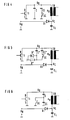
- FIG. 1 shows a section of the circuit of a known flyback switching power supply, in which a capacitor is connected in parallel with the semiconductor switching element as a snubber circuit.
- FIG. 2 shows a representation as in FIG. 1, in which an RCD circuit is provided as the snubber circuit.
- FIGS. 1 and 2 shows the time course of the voltage drop across the load path of the semiconductor switching element in FIGS. 1 and 2 in switching operation.
- FIG. 4 shows a detail of a first exemplary embodiment of a circuit arrangement according to the invention of a flyback switching power supply, in which a capacitance is connected in parallel with the semiconductor switching element and this capacitance can be changed.
- FIG. 5 shows a second exemplary embodiment of a circuit arrangement according to the invention with an RCD circuit as a snubber circuit in which the capacitance can be changed.
- FIG. 6 shows a third exemplary embodiment of a flyback converter switched-mode power supply according to the invention, in which two capacitors are connected in series with the semiconductor switching element and one of these capacitors can be bridged by a switching device.
- FIG. 7 shows a representation similar to FIG. 6, in which an RCD circuit is provided as a snubber circuit, the capacitance of which can be changed.
- FIG. 9 shows a complete circuit diagram of a flyback converter switching power supply according to the invention with a bipolar transistor as a switching device for changing the capacitance of the capacitive device.
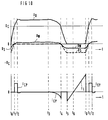
- FIG. 10 shows the voltages and currents occurring in the switched-mode power supply shown in FIG.
- FIG. 11 shows a second embodiment of a flyback switching power supply according to the invention with a MOS transistor as a switching device for changing the capacitance of the capacitive device.
- U N in the FIG designates an AC voltage to be rectified, which is connected to a smoothing capacitor C L via a rectifier device which is shown only as a diode DI for the sake of simplicity.
- the smoothing capacitor C L lies between the cathode connection at the diode DI and the reference potential.
- a direct voltage U C can be tapped at the connection point of the diode DI and the smoothing capacitor C L.
- the cathode connection of the diode DI is connected via a primary winding n P of a transformer TR to the load path of a semiconductor switching element T1.
- a MOS transistor is provided as the semiconductor switching element T1, the source terminal S of which is at reference potential and the drain terminal D of which is connected to a second terminal of the primary winding n P.
- the semiconductor switching element T1 switches the rectified voltage U C to the primary winding n P of the transformer TR in a pulse-width-modulated manner.
- a so-called snubber circuit in parallel to the load path D, S of the semiconductor switching element T1.
- a capacitor C is provided as the snubber circuit, which is connected in parallel with the load path D, S of the semiconductor switching element T1.
- This capacitor C can have a capacitance of 100 pF to 10 nF, for example.
- FIG. 2 shows a section of a further known circuit arrangement of a flyback converter switching power supply, which differs from the circuit in FIG. 1 only in that not only a capacitor connected in parallel, but an RCD circuit is provided as the snubber circuit.
- This RCD circuit has a series connection of a capacitor C * with a resistor R *, the resistor R * being connected to reference potential with a connection, while an opposite connection is connected to a connection of the capacitor C *.
- a second connection of this capacitor C * is connected to a connection point of the primary winding n P of the transformer TR and the drain connection of the semiconductor switching element T1.
- the capacitor C * can again have a capacitance of 100 pF to 10nF, the resistor R * has a low resistance (approximately 2 to 20 ohms, the diode D * only has to be voltage-proof accordingly.
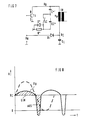
- FIG. 1 and FIG. 2 have hitherto been used in flyback switching power supplies to avoid overshoots or to attenuate them. Their mode of operation is shown in this way. Due to the parallel capacitance C or the capacitance C * in the RCD circuit and a primary inductance of the primary winding n P of the transformer TR, the load voltage U D oscillates after the semiconductor switching element T1 has been switched on and off as shown in FIG 3. It can be seen that the peak value of the voltage U D dropping across the semiconductor switching element T1 must be at least twice as large as the voltage U C to be switched if the load voltage U D is to pass through the zero line after the oscillation.
- the capacitance of the capacitive device can be changed at least from a first value to a smaller second value if the voltage U D falling across the load path D, S of the semiconductor switching element T1 is less than the DC voltage U C , which to be switched.
- FIG 4 differs in the representation of FIG 1 in that in addition to parallel Load path D, S of the semiconductor switching element T1, another capacitor CC is connected with a switching device SC connected in series. If the switching device SC is closed, a greater capacitance is present parallel to the load path D, S of the semiconductor switching element T1 than if the switching device SC were open.
- This switching device SC is always switched on according to the invention when the voltage U D falling across the load path of the semiconductor switching element T1 is greater than the voltage U C to be switched.
- the circuit arrangement in FIG. 5 differs from the arrangement in FIG. 4 in that an RCD circuit is provided there as a snubber circuit.
- the RCD circuit shown in FIG. 2 with the capacitor C *, the resistor R * with a diode D * connected in parallel is expanded by the series connection of a capacitor CC * with a series-connected switching device SC, which are together in parallel with the capacitor C *.
- the control takes place under the same time condition as in the circuit of FIG. 4, ie the switching device SC is closed when the voltage U D falling across the load path D, S of the semiconductor switching element T1 is greater than the DC voltage U C to be switched.
- FIG. 6 shows a third possible embodiment of the circuit arrangement according to the invention.
- the two capacitors C and CC are not connected in parallel to one another, but rather in series with one another.
- the switching device SC is parallel to one of these capacitors. If the switching device SC is closed, the total capacitance of these capacitors C and CC is greater than if the switching device SC is open. In the circuit arrangement shown in FIG. 6, the switching device SC is therefore always closed when the voltage U D falling across the load path D, S of the semiconductor switching element D1 is greater than the DC voltage U C to be switched.
- an RCD circuit with the capacitor C *, the diode D * and the resistor R * is again provided as a snubber circuit.
- the parallel connection of a capacitor CC * with the switching device SC is connected between the capacitor C * and the parallel connection of the diode D * and the resistor R *.
- This switching device SC is switched on and off under the same time conditions as already explained in connection with FIGS. 4, 5 and 6.
- the capacitors C and C * or the switched capacitors CC and CC * are to be dimensioned as follows.
- the switched capacitors CC and CC * should be the same size or larger than the non-switched capacitors C and C *.
- the capacitors C and C * can have a capacitance of the order of about 100 pF to a few 100 nF.
- the switching device SC in the examples of FIGS. 4 to 7 is always closed according to the invention when the load voltage U D is greater or approximately greater than the DC voltage U C to be switched, the time profile of the load voltage U D shown in FIG. 8 results.
- the voltage U D crosses the zero line, although its peak value only slightly exceeds U C.
- the switching device SC is opened and the oscillation frequency of the flyback converter switched-mode power supply is higher, since a smaller capacitance is effective as the resonant circuit capacitance. It can be clearly seen in FIG. 8 that the voltage U D crosses the zero line.
- the capacitor CC or CC * to be switched is sufficiently large and the turns ratio of primary windings to secondary windings of the transformer TR is selected appropriately. If the capacitor C or C * and the capacitor CC or CC * to be switched are selected to be the same size, the turns ratio of the primary winding must be n P to be secondary winding 1 / ⁇ 2, so that U D just reaches the zero line and thus it is ensured that the semiconductor switching element T1 can switch on without voltage. This applies to a desired voltage ratio of 1: 1 between the primary and secondary side of the transformer TR.
- the hatched areas in FIG. 8 for switching on and switching off are of the same size. These represent the voltage-time product.
- FIG. 9 shows an example of a flyback switching power supply according to the invention in detail. Except for the differences to be described below, this flyback converter switched-mode power supply is described, for example, in the Siemens product information "Function and application of flyback converter IC TDA 4605", order no. B111-B6090.
- the circuit shown in FIG. 9 has, according to the invention, a further primary-side winding n W which, for example, consists of only one or two windings and is polarized in the opposite direction to the primary winding n P.
- the respective sense of polarity is shown in FIG. 9 by a point on the primary or secondary windings.
- This further winding n W is connected with a connection via a resistor R to a base connection of a bipolar transistor acting as a switching device SC. Its other connection is connected to an emitter connection of this bipole transistor and, on the other hand, via a capacitor CC to the drain connection of the MOS transistor, which is the semiconductor switching element T1.
- the switching device SC thus consists of an NPN transistor, an inverse diode DS connected in parallel with this - which can already be integrated in the transistor - and the resistor R which acts as a basic series resistor.
- This transistor which acts as a switch, is driven by the further winding n W of the transformer TR.
- n W a winding already present on the transformer TR can also be used, provided that it has the corresponding sense of polarity.
- the diode DS derives the current flowing in the opposite direction through the capacitor CC.
- a PNP transistor can of course also be used, provided that its base connection is connected to the other connection of the further winding n W.
- U C means the voltage to be switched to the primary winding n P by the semiconductor switching element T1
- U D the load voltage dropping at the conductor switching element T1
- U W the voltage at the further winding n W of the transformer TR
- I L a load current flowing through the semiconductor switching element T1
- I CP a current flowing through the switching device SC.
- the semiconductor switching element T1 is switched off in accordance with control signals from the control circuit IC, in the illustration of FIG. 9 the integrated circuit TDA 4605 from Siemens.
- the transformer TR is charged and the load voltage U D rises steeply until time t1 because of the high energy stored in the transformer TR and reaches a potential which corresponds to the voltage UC to be switched.
- the voltage UW on the further winding nW of the transformer TR becomes positive and switches the switching device SC through, as a result of which the capacitor CC is connected in parallel with the capacitor C and thereby the capacitance of the capacitive device of the Snubber circuit connected in parallel with the semiconductor switching element T1 is increased. This slows down the increase in load voltage U D something.
- the load voltage U D remains at the same level and the transformer TR begins to discharge again on the secondary side. The discharge is completed at time t3.
- the load voltage U D initially drops slowly.
- the transformer TR receives the necessary return energy from the capacitor CC, which was switched on by the switching device SC.
- the voltage U W becomes negative and the switching device SC is switched off.
- the load voltage U D drops faster and reaches zero volts at time t5.
- An inverse current I L flows through the inverse diode DS between the times t5 and t6.
- the semiconductor switching element T1 Since the semiconductor switching element T1 is switched on again at the time t5 by the control circuit IC — in accordance with a zero crossing detection signal — the load voltage U D remains at zero volts and the load current I L becomes positive again at the time t6.
- the transformer TR charges up until the semiconductor switching element T1 is switched off again by the control circuit IC at the new time t0 and a new cycle begins.
- the zero crossing detection signal for the control circuit IC can be derived exactly from the load voltage U D itself, since the load voltage U D always crosses the zero line.
- FIG. 11 shows a further example of a switching power supply according to the invention.
- This circuit arrangement differs from that shown in FIG. 9 only in that a MOS transistor is now used as the switching device SC.
- This MOS transistor is connected with its gate terminal G and with its source terminal S to the further winding n W in the manner shown in FIG.
- the drain terminal D of the MOS transistor of the switching device SC is connected to the reference potential and an inverse diode DS is connected in parallel with this switching device SC.
- the series resistor R compared to the bipolar transistor. Otherwise, the circuit arrangement in FIG. 11 does not differ from the circuit arrangement in FIG. 9.
- the courses of the individual signals also correspond to the course in FIG. 10.
Landscapes
- Engineering & Computer Science (AREA)
- Power Engineering (AREA)
- Dc-Dc Converters (AREA)
Claims (5)
- Alimentation à découpage à accumulation comportant un élément (T1) de commutation à semiconducteur, qui comporte une section (D, S) de charge qui est reliée, pour l'application cadencée d'une tension (UC) continue à un premier enroulement primaire (np) d'un transformateur (TR), à une borne de l'enroulement primaire (np), à l'autre borne duquel peut être appliquée la tension continue (UC), un dispositif (IC) de commande pour la commande de l'élément (T1) de commutation à semiconducteur ainsi qu'à un dispositif (C ; D*, R*, C*) capacitif branché en parallèle avec la section de charge (D, S) de l'élément (T1) de commutation à semiconducteur,
caractérisée en ce que
une première valeur petite et une seconde valeur plus grande de la capacité du dispositif capacitif (C; D*, R*, C*) peut être branchée, il est prévu un enroulement supplémentaire (nW) couplé au premier enroulement primaire (np), qui fait que la capacité du dispositif capacitif (C ; D*, R*, C*) est branchée de la première valeur à la seconde valeur, lorsque qu'une chute de tension (UD) sur la section de charge (D, S) de l'élément (T1) de commutation à semiconducteur est plus grande, au moins approximativement, que la tension continue (UC) et que la capacité du dispositif capacitif (C ; D*, R*, C*) passe de la seconde valeur à la première valeur, lorsque la chute de tension (UC) sur la section (D, S) de charge de l'élément (T1) de commutation à semiconducteur est plus petite, au moins approximativement, que la tension continue (UC). - Alimentation à découpage à accumulation suivant la revendication 1,
caractérisée en ce que
le dispositif capacitif (C ; D*, R*, C*) est un condensateur (C). - Alimentation à découpage à accumulation suivant la revendication 1,
caractérisée en ce que
le dispositif capacitif (C ; D*, R*, C*) est le circuit-série d'un transformateur (C*) et d'un circuit parallèle constitué d'une diode (D*) et d'une résistance (R*). - Alimentation à découpage à accumulation suivant l'une des revendications 1 à 3,
caractérisée en ce que
le dispositif capacitif (C ; D*, R*, C*) comporte au moins deux condensateurs (C, CC) branchés en série, et l'un de ces condensateurs (CC) peut être court-circuité par l'intermédiaire d'un dispositif (SC) d'interruption commandé par l'enroulement supplémentaire (nW). - Alimentation à découpage à accumulation suivant l'une des revendications 1 à 4,
caractérisée en ce que
le dispositif capacitif (C ; D*, R*, C*) comporte au moins deux condensateurs (C, CC) branchés en parallèle entre eux, au moins l'un de ces condensateurs pouvant être débranché par l'intermédiaire d'un second dispositif (SC) d'interruption commandé par l'enroulement supplémentaire (nW).
Priority Applications (3)
| Application Number | Priority Date | Filing Date | Title |
|---|---|---|---|
| AT93102866T ATE152302T1 (de) | 1993-02-24 | 1993-02-24 | Sperrwandler-schaltnetzteil mit einem halbleiterschaltelement geringer spannungsfestigkeit |
| EP93102866A EP0613232B1 (fr) | 1993-02-24 | 1993-02-24 | Convertisseur à récupération avec un interrupteur à semi-conducteur de base tenue en tension |
| DE59306269T DE59306269D1 (de) | 1993-02-24 | 1993-02-24 | Sperrwandler-Schaltnetzteil mit einem Halbleiterschaltelement geringer Spannungsfestigkeit |
Applications Claiming Priority (1)
| Application Number | Priority Date | Filing Date | Title |
|---|---|---|---|
| EP93102866A EP0613232B1 (fr) | 1993-02-24 | 1993-02-24 | Convertisseur à récupération avec un interrupteur à semi-conducteur de base tenue en tension |
Publications (2)
| Publication Number | Publication Date |
|---|---|
| EP0613232A1 EP0613232A1 (fr) | 1994-08-31 |
| EP0613232B1 true EP0613232B1 (fr) | 1997-04-23 |
Family
ID=8212630
Family Applications (1)
| Application Number | Title | Priority Date | Filing Date |
|---|---|---|---|
| EP93102866A Expired - Lifetime EP0613232B1 (fr) | 1993-02-24 | 1993-02-24 | Convertisseur à récupération avec un interrupteur à semi-conducteur de base tenue en tension |
Country Status (3)
| Country | Link |
|---|---|
| EP (1) | EP0613232B1 (fr) |
| AT (1) | ATE152302T1 (fr) |
| DE (1) | DE59306269D1 (fr) |
Families Citing this family (4)
| Publication number | Priority date | Publication date | Assignee | Title |
|---|---|---|---|---|
| GB9321912D0 (en) * | 1993-10-23 | 1993-12-15 | Nicotech Ltd | Inverter circuits |
| AU2002345266B2 (en) | 2002-07-08 | 2009-07-02 | Ranbaxy Laboratories Limited | 3,6-disubstituted azabicyclo [3.1.0]hexane derivatives useful as muscarinic receptor antagonists |
| WO2004089898A1 (fr) | 2003-04-09 | 2004-10-21 | Ranbaxy Laboratories Limited | Derives d'azabicyclo hexane substitues en tant qu'antagonistes de recepteurs muscariniques |
| CN100436414C (zh) | 2003-04-11 | 2008-11-26 | 兰贝克赛实验室有限公司 | 作为毒蕈碱受体拮抗剂的氮杂双环衍生物 |
Family Cites Families (4)
| Publication number | Priority date | Publication date | Assignee | Title |
|---|---|---|---|---|
| FR2592996B1 (fr) * | 1986-01-13 | 1992-12-24 | Telemecanique Electrique | Interrupteur statique blocable pour circuit electrique alternatif comprenant une charge inductive. |
| JPH0748944B2 (ja) * | 1989-10-14 | 1995-05-24 | 東光株式会社 | Dc―dcコンバータ |
| US4959764A (en) * | 1989-11-14 | 1990-09-25 | Computer Products, Inc. | DC/DC converter switching at zero voltage |
| US5126931A (en) * | 1990-09-07 | 1992-06-30 | Itt Corporation | Fixed frequency single ended forward converter switching at zero voltage |
-
1993
- 1993-02-24 AT AT93102866T patent/ATE152302T1/de not_active IP Right Cessation
- 1993-02-24 DE DE59306269T patent/DE59306269D1/de not_active Expired - Fee Related
- 1993-02-24 EP EP93102866A patent/EP0613232B1/fr not_active Expired - Lifetime
Also Published As
| Publication number | Publication date |
|---|---|
| DE59306269D1 (de) | 1997-05-28 |
| EP0613232A1 (fr) | 1994-08-31 |
| ATE152302T1 (de) | 1997-05-15 |
Similar Documents
| Publication | Publication Date | Title |
|---|---|---|
| DE60027538T2 (de) | Überspannungsgeschützter Stromwechselrichter mit einem spannungsgesteuerten Schaltkreis | |
| DE69111738T2 (de) | Verlustfreier Dämpfungskreis. | |
| DE69729294T2 (de) | Niedrigpreis-, Hochspannungs-, Flyback-Stromversorgung | |
| DE69009359T2 (de) | Leistungsquellevorrichtung. | |
| EP0498917B1 (fr) | Convertisseur commandé par horloge avec limitation de courant | |
| DE4210092A1 (de) | Daempfungsschaltung fuer leistungswandler | |
| DE3126525A1 (de) | "spannungsgesteuerter halbleiterschalter und damit versehene spannungswandlerschaltung" | |
| DE3914799A1 (de) | Durchflusswandler | |
| DE4421249C2 (de) | Schaltstromversorgungsgerät mit Snubber-Schaltung | |
| DE2207203A1 (de) | Chopper-Umformer | |
| DE3213869C2 (de) | Selbstschwingender Sekundärschaltregler | |
| DE3741221C1 (de) | Anordnung zum Befreien eines Halbleiterschalters vor hoher Sperrspannungsbeanspruchung sowie Anwendung hierzu | |
| DE102018132214A1 (de) | Steuerschaltung für eine Oszillatorschaltung zum Betrieb von parallelgespeisten Oszillatoren | |
| DE69720176T2 (de) | Stromversorgungsschaltung | |
| EP0613232B1 (fr) | Convertisseur à récupération avec un interrupteur à semi-conducteur de base tenue en tension | |
| DE10041475C2 (de) | Schaltnetzteil | |
| DE4205599B4 (de) | Halbbrücken-Wechselrichter oder eine von einem Vollbrücken-Wechselrichter durch Halbierungsberechnung abgeleitete Schaltungsanordnung in Form eines Halbbrücken-Wechselrichters sowie Verfahren zu deren Steuerung | |
| EP0464246A1 (fr) | Agencement de circuit pour une alimentation à découpage du type à récupération oscillant librement | |
| DE10257908A1 (de) | Getaktete Leistungsversorgung | |
| DE4447406C1 (de) | GTO-Stromrichter mit weicher Kommutierung | |
| DE4135569C1 (fr) | ||
| DE2716367A1 (de) | Schutzbeschaltung fuer einen transistor | |
| DE10146900A1 (de) | Schaltungsanordnung und Verfahren zur potentialgetrennten Ansteuerung in Serie geschalteter, abschaltbarer Halbleiterschaltelemente | |
| EP2140735B1 (fr) | Ensemble circuit servant à amorcer et à faire fonctionner au moins une lampe à décharge | |
| DE2443892B1 (de) | Schaltungsanordnung zur Herabsetzung der auftretenden Verlustleistung beim Abschalten einer wenigstens einen Halbleiterschalter und eine Induktanz enthaltenden Reihenschaltung |
Legal Events
| Date | Code | Title | Description |
|---|---|---|---|
| PUAI | Public reference made under article 153(3) epc to a published international application that has entered the european phase |
Free format text: ORIGINAL CODE: 0009012 |
|
| AK | Designated contracting states |
Kind code of ref document: A1 Designated state(s): AT BE CH DE DK ES FR GB GR IE IT LI LU MC NL PT SE |
|
| RBV | Designated contracting states (corrected) |
Designated state(s): AT DE FR GB IT |
|
| 17P | Request for examination filed |
Effective date: 19950119 |
|
| 17Q | First examination report despatched |
Effective date: 19950822 |
|
| GRAG | Despatch of communication of intention to grant |
Free format text: ORIGINAL CODE: EPIDOS AGRA |
|
| GRAH | Despatch of communication of intention to grant a patent |
Free format text: ORIGINAL CODE: EPIDOS IGRA |
|
| GRAH | Despatch of communication of intention to grant a patent |
Free format text: ORIGINAL CODE: EPIDOS IGRA |
|
| GRAA | (expected) grant |
Free format text: ORIGINAL CODE: 0009210 |
|
| AK | Designated contracting states |
Kind code of ref document: B1 Designated state(s): AT DE FR GB IT |
|
| PG25 | Lapsed in a contracting state [announced via postgrant information from national office to epo] |
Ref country code: FR Free format text: THE PATENT HAS BEEN ANNULLED BY A DECISION OF A NATIONAL AUTHORITY Effective date: 19970423 |
|
| REF | Corresponds to: |
Ref document number: 152302 Country of ref document: AT Date of ref document: 19970515 Kind code of ref document: T |
|
| REF | Corresponds to: |
Ref document number: 59306269 Country of ref document: DE Date of ref document: 19970528 |
|
| ET | Fr: translation filed | ||
| GBT | Gb: translation of ep patent filed (gb section 77(6)(a)/1977) |
Effective date: 19970627 |
|
| PG25 | Lapsed in a contracting state [announced via postgrant information from national office to epo] |
Ref country code: GB Free format text: LAPSE BECAUSE OF NON-PAYMENT OF DUE FEES Effective date: 19980224 Ref country code: AT Free format text: LAPSE BECAUSE OF NON-PAYMENT OF DUE FEES Effective date: 19980224 |
|
| PLBE | No opposition filed within time limit |
Free format text: ORIGINAL CODE: 0009261 |
|
| STAA | Information on the status of an ep patent application or granted ep patent |
Free format text: STATUS: NO OPPOSITION FILED WITHIN TIME LIMIT |
|
| 26N | No opposition filed | ||
| GBPC | Gb: european patent ceased through non-payment of renewal fee |
Effective date: 19980224 |
|
| PG25 | Lapsed in a contracting state [announced via postgrant information from national office to epo] |
Ref country code: DE Free format text: LAPSE BECAUSE OF NON-PAYMENT OF DUE FEES Effective date: 19981103 |
|
| REG | Reference to a national code |
Ref country code: FR Ref legal event code: ST |
|
| PG25 | Lapsed in a contracting state [announced via postgrant information from national office to epo] |
Ref country code: IT Free format text: LAPSE BECAUSE OF NON-PAYMENT OF DUE FEES;WARNING: LAPSES OF ITALIAN PATENTS WITH EFFECTIVE DATE BEFORE 2007 MAY HAVE OCCURRED AT ANY TIME BEFORE 2007. THE CORRECT EFFECTIVE DATE MAY BE DIFFERENT FROM THE ONE RECORDED. Effective date: 20050224 |