EP0609014A2 - Method of forming contacts to source and drains regions - Google Patents
Method of forming contacts to source and drains regions Download PDFInfo
- Publication number
- EP0609014A2 EP0609014A2 EP94300406A EP94300406A EP0609014A2 EP 0609014 A2 EP0609014 A2 EP 0609014A2 EP 94300406 A EP94300406 A EP 94300406A EP 94300406 A EP94300406 A EP 94300406A EP 0609014 A2 EP0609014 A2 EP 0609014A2
- Authority
- EP
- European Patent Office
- Prior art keywords
- conductor
- edge
- substrate
- patterned
- layer
- Prior art date
- Legal status (The legal status is an assumption and is not a legal conclusion. Google has not performed a legal analysis and makes no representation as to the accuracy of the status listed.)
- Granted
Links
- 238000000034 method Methods 0.000 title claims abstract description 21
- 239000004020 conductor Substances 0.000 claims abstract description 26
- 239000000758 substrate Substances 0.000 claims abstract description 26
- 229910021420 polycrystalline silicon Inorganic materials 0.000 claims abstract description 16
- 229920005591 polysilicon Polymers 0.000 claims abstract description 16
- 229910021332 silicide Inorganic materials 0.000 claims abstract description 15
- FVBUAEGBCNSCDD-UHFFFAOYSA-N silicide(4-) Chemical compound [Si-4] FVBUAEGBCNSCDD-UHFFFAOYSA-N 0.000 claims abstract description 15
- 239000004065 semiconductor Substances 0.000 claims abstract description 7
- 238000004519 manufacturing process Methods 0.000 claims abstract description 6
- 238000000059 patterning Methods 0.000 claims abstract description 5
- 239000000463 material Substances 0.000 claims description 11
- VYPSYNLAJGMNEJ-UHFFFAOYSA-N Silicium dioxide Chemical compound O=[Si]=O VYPSYNLAJGMNEJ-UHFFFAOYSA-N 0.000 claims description 10
- 238000005530 etching Methods 0.000 claims description 7
- 235000012239 silicon dioxide Nutrition 0.000 claims description 5
- 239000000377 silicon dioxide Substances 0.000 claims description 5
- 239000003870 refractory metal Substances 0.000 claims description 3
- BOTDANWDWHJENH-UHFFFAOYSA-N Tetraethyl orthosilicate Chemical compound CCO[Si](OCC)(OCC)OCC BOTDANWDWHJENH-UHFFFAOYSA-N 0.000 claims description 2
- WQJQOUPTWCFRMM-UHFFFAOYSA-N tungsten disilicide Chemical group [Si]#[W]#[Si] WQJQOUPTWCFRMM-UHFFFAOYSA-N 0.000 claims description 2
- 229910021342 tungsten silicide Inorganic materials 0.000 claims description 2
- 229920002120 photoresistant polymer Polymers 0.000 description 14
- XUIMIQQOPSSXEZ-UHFFFAOYSA-N Silicon Chemical compound [Si] XUIMIQQOPSSXEZ-UHFFFAOYSA-N 0.000 description 8
- 229910052710 silicon Inorganic materials 0.000 description 8
- 239000010703 silicon Substances 0.000 description 8
- 239000003989 dielectric material Substances 0.000 description 2
- 239000002019 doping agent Substances 0.000 description 2
- 238000005468 ion implantation Methods 0.000 description 2
- 230000015572 biosynthetic process Effects 0.000 description 1
- 238000010586 diagram Methods 0.000 description 1
- 238000009792 diffusion process Methods 0.000 description 1
- 230000005669 field effect Effects 0.000 description 1
- -1 for example Chemical compound 0.000 description 1
- 230000015654 memory Effects 0.000 description 1
- 230000003068 static effect Effects 0.000 description 1
- 238000012800 visualization Methods 0.000 description 1
Images


Classifications
-
- H—ELECTRICITY
- H01—ELECTRIC ELEMENTS
- H01L—SEMICONDUCTOR DEVICES NOT COVERED BY CLASS H10
- H01L21/00—Processes or apparatus adapted for the manufacture or treatment of semiconductor or solid state devices or of parts thereof
- H01L21/70—Manufacture or treatment of devices consisting of a plurality of solid state components formed in or on a common substrate or of parts thereof; Manufacture of integrated circuit devices or of parts thereof
- H01L21/71—Manufacture of specific parts of devices defined in group H01L21/70
- H01L21/768—Applying interconnections to be used for carrying current between separate components within a device comprising conductors and dielectrics
- H01L21/76838—Applying interconnections to be used for carrying current between separate components within a device comprising conductors and dielectrics characterised by the formation and the after-treatment of the conductors
- H01L21/76886—Modifying permanently or temporarily the pattern or the conductivity of conductive members, e.g. formation of alloys, reduction of contact resistances
- H01L21/76889—Modifying permanently or temporarily the pattern or the conductivity of conductive members, e.g. formation of alloys, reduction of contact resistances by forming silicides of refractory metals
-
- H—ELECTRICITY
- H01—ELECTRIC ELEMENTS
- H01L—SEMICONDUCTOR DEVICES NOT COVERED BY CLASS H10
- H01L21/00—Processes or apparatus adapted for the manufacture or treatment of semiconductor or solid state devices or of parts thereof
- H01L21/02—Manufacture or treatment of semiconductor devices or of parts thereof
- H01L21/04—Manufacture or treatment of semiconductor devices or of parts thereof the devices having potential barriers, e.g. a PN junction, depletion layer or carrier concentration layer
- H01L21/18—Manufacture or treatment of semiconductor devices or of parts thereof the devices having potential barriers, e.g. a PN junction, depletion layer or carrier concentration layer the devices having semiconductor bodies comprising elements of Group IV of the Periodic Table or AIIIBV compounds with or without impurities, e.g. doping materials
- H01L21/28—Manufacture of electrodes on semiconductor bodies using processes or apparatus not provided for in groups H01L21/20 - H01L21/268
- H01L21/283—Deposition of conductive or insulating materials for electrodes conducting electric current
- H01L21/285—Deposition of conductive or insulating materials for electrodes conducting electric current from a gas or vapour, e.g. condensation
- H01L21/28506—Deposition of conductive or insulating materials for electrodes conducting electric current from a gas or vapour, e.g. condensation of conductive layers
- H01L21/28512—Deposition of conductive or insulating materials for electrodes conducting electric current from a gas or vapour, e.g. condensation of conductive layers on semiconductor bodies comprising elements of Group IV of the Periodic Table
- H01L21/28518—Deposition of conductive or insulating materials for electrodes conducting electric current from a gas or vapour, e.g. condensation of conductive layers on semiconductor bodies comprising elements of Group IV of the Periodic Table the conductive layers comprising silicides
-
- H—ELECTRICITY
- H01—ELECTRIC ELEMENTS
- H01L—SEMICONDUCTOR DEVICES NOT COVERED BY CLASS H10
- H01L21/00—Processes or apparatus adapted for the manufacture or treatment of semiconductor or solid state devices or of parts thereof
- H01L21/02—Manufacture or treatment of semiconductor devices or of parts thereof
- H01L21/04—Manufacture or treatment of semiconductor devices or of parts thereof the devices having potential barriers, e.g. a PN junction, depletion layer or carrier concentration layer
- H01L21/18—Manufacture or treatment of semiconductor devices or of parts thereof the devices having potential barriers, e.g. a PN junction, depletion layer or carrier concentration layer the devices having semiconductor bodies comprising elements of Group IV of the Periodic Table or AIIIBV compounds with or without impurities, e.g. doping materials
- H01L21/28—Manufacture of electrodes on semiconductor bodies using processes or apparatus not provided for in groups H01L21/20 - H01L21/268
- H01L21/283—Deposition of conductive or insulating materials for electrodes conducting electric current
- H01L21/285—Deposition of conductive or insulating materials for electrodes conducting electric current from a gas or vapour, e.g. condensation
- H01L21/28506—Deposition of conductive or insulating materials for electrodes conducting electric current from a gas or vapour, e.g. condensation of conductive layers
- H01L21/28512—Deposition of conductive or insulating materials for electrodes conducting electric current from a gas or vapour, e.g. condensation of conductive layers on semiconductor bodies comprising elements of Group IV of the Periodic Table
- H01L21/28525—Deposition of conductive or insulating materials for electrodes conducting electric current from a gas or vapour, e.g. condensation of conductive layers on semiconductor bodies comprising elements of Group IV of the Periodic Table the conductive layers comprising semiconducting material
Definitions
- This invention relates generally to a method of making semiconductor integrated circuits and particularly to a method which forms contacts to sources or drains.
- SRAMs Static Random Access Memories
- the junctions denoted by reference numerals 11 and 13 provide instances in which, for example, the gate of pull-down transistor 15 is connected to the source/drain of access transistor 19 or, the gate of pull-down transistor 17 is connected to the source/drain of access transistor 21.
- one of the connections (11 or 15) is made at the so-called "poly-1" level. That is, the polysilicon which forms the gate of the respective pull-down transistor is patterned over the source/drain region of the access transistor, thereby forming a direct contact.
- the other access/pull-down connection is often made at a higher level of the integrated circuit (i.e., perhaps at the "poly-2" level or higher).
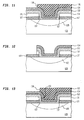
- FIGS. 2-5 illustrate a problem which occurs when a polysilicon gate is patterned directly over a source/drain.
- reference numeral 23 denotes a substrate which may be, typically, silicon, epitaxial silicon, doped silicon, etc. In general, the term substrate refers to a material or to a layer upon which other materials may be subsequently formed.
- Reference numeral 25 denotes a junction region which comprises the source or drain of an access transistor, such as transistors 19 or 21 in FIG. 1.
- Reference numeral 27 denotes a dielectric layer which, typically, may be silicon dioxide or silicon oxynitride. If layer 27 is silicon dioxide, it may typically have a thickness of approximately 100 ⁇ . In FIG. 3, layer 27 has been patterned exposing surface 29 of junction 25. In FIG.
- polysilicon layer 31 has been deposited to cover exposed surface 29 of junction 25. It is desired that polysilicon layer 31 should be patterned using a photoresist. Photoresist 33 is subsequently deposited over polysilicon layer 31 and patterned. It is desirable that edge 35 of photoresist 33 be immediately above (or, in FIG. 4, to the left of) edge 37 of patterned dielectric 27.
- edge 35 of photoresist 33 be slightly misaligned (and, as shown in FIG. 4, somewhat to the right of edge 37 of dielectric 27, i.e., should edge 35 overlie the opening defined by edge 37 of dielectric 27), subsequent exposure of polysilicon layer 31 to an etchant species may cause trenching into junction 25 of substrate 23. The trenching may damage the electrical characteristics of the junction and, under worst circumstances, may completely penetrate junction 25.
- FIGS. 4 and 5 shows that, if patterned edge 35 of resist 33 is positioned parallel with, or to the left of, patterned edge 37 of dielectric 27 (i.e., edge 35 overlies layer 27), subsequent etching will stop on dielectric 27 and not damage junction 25.
- the trench 39 depicted in FIG. 5 may be obtained.
- the trenching problem is addressed by this invention which illustratively includes: forming a patterned dielectric over a substrate, the patterned dielectric exposing a portion of the substrate; forming a patterned first conductor over the patterned dielectric, the first conductor not contacting the substrate; forming a second conductor layer over the first patterned conductor; forming a material layer over the second conductor; patterning the material layer, thereby creating an edge of the material layer and exposing a portion of the second conductor; and etching the exposed portion of the second conductor.
- the first conductor is a poly 1 conductor which is patterned so it does not contact the substrate.
- the second conductor is a silicide which serves to connect the poly 1 and the substrate.
- reference numeral 123 designates a substrate which may typically be silicon, epitaxial silicon, or doped silicon.
- Doped region 125 may be formed, for example, by diffusion or ion implantation. Alternatively, doped region 125 may be formed at a later stage in the process by driving dopants out from subsequently formed silicide layers. For convenience in visualization, doped region 125 is depicted at the early stage of the inventive process.
- Layer 127 is a dielectric layer, typically silicon dioxide, having a thickness of approximately 100 ⁇ or, possibly, silicon oxynitride.
- Layer 131 is desirably a conductor such as polysilicon, typically having a thickness of approximately 1000 ⁇ .
- layers 127 and 131 are formed during the early stages of semiconductor integrated circuit processing. Both layers 127 and 131 may, in other parts of the integrated circuit, comprise respectively a gate oxide and gate conductor.
- layers 127 and 131 have been patterned, exposing surface 129 of substrate 123. It is desired to make a patterned electrical connection between layer 131 and surface 129.
- blanket layers of a refractory metal silicide for example, tungsten silicide 132, and a dielectric 134, for example, plasma-enhanced TEOS or BPTEOS may be deposited.
- a refractory metal silicide for example, tungsten silicide 132
- a dielectric 134 for example, plasma-enhanced TEOS or BPTEOS
- silicide 132 may be doped, perhaps by ion implantation.
- An anneal may be performed to drive the dopants from silicide 132 into substrate 123, thereby forming junction region 125 (which has been depicted since FIG. 6 for conceptual convenience).
- edges 132 and 134 are co-linear with (or to the left of) the edges of dielectrics 131 and 127. That is, turning to FIG. 9, after photoresist 135 is deposited and spun, photoresist 135 is patterned creating edge 136. Ideally, edge 136 is co-linear with edge 137 of layers 131 and 127, respectively. Should edge 136 be co-linear with edge 137, turning to FIG. 10, layer 134 may be etched to create a hard mask and, subsequently, layer 132 may be etched with the aid of the hard mask to create patterned conductor 138 with patterned edge 139 which precisely abuts edge 137 of layers 131 and 127.
- edge 136 is precisely co-linear with edge 137 of layers 131 and 127.
- edge 136 will be to the left of edge 137; on other occasions, edge 136 may be positioned to the right of edge 137.
- edge 136 may be described as overlying edge 137, which defines an opening over substrate 123.
- FIGS. 11 and 12 illustrate what happens when edge 136 of photoresist 135 is positioned, because of misalignment tolerances, to the left of edge 137. In other words, patterned edge 136 of photoresist 135 does not overlie the opening created by edge 137 over substrate 123.
- FIGS. 11 and 12 after the patterning of resist 135, an anisotropic etch is performed, thereby forming the configuration depicted in FIG. 12. It will be noted that polysilicon layer 131 is etched together with silicide layer 132 and dielectric 134. Subsequent processing may be employed to remove dielectric 134, if desired.
- An alternative method of etching is to etch a hard mask into dielectric 134 and then, employing the hard-mask technique, etch underlying layers 132 and 131.
- edge 136 of photoresist 134 is slightly interior to edges 137. That is, edge overlies the opening over substrate 123 defined by edge 137. In FIG. 13, edge 136 overlies the vertical sidewall 150 of silicide layer 132.
- FIG. 14 After etching of layers 134 and 132 is completed, the configuration depicted in FIG. 14 is obtained. It will be noted, examination of FIG. 14 shows that the sidewall portion 150 of silicide layer 134 has protected substrate 123 against trenching (unlike the case depicted in FIG. 5). Etching of layers 134 and 132 produces a flat surface 151 in silicide 134 which is roughly parallel with upper surface 153 of polysilicon layer 131.
- FIG. 15 further etching has been performed to remove that portion of polysilicon layer 131 at the left-most part of the figure and to remove dielectric 134. Again, examination of FIG. 15 shows that the presence of sidewall 150 has prevented trenching of the substrate.
- FIGS. 16, 17, and 18 depict an example of somewhat greater misalignment.
- edge 136 of resist 135 is positioned interior to edge 137. Furthermore, edge 136 of resist 135 is interior to edge 150 of silicide layer 132. In FIG. 17, layers 134 and 132 are etched (with or without hard-mask techniques). Finally, in FIG. 18, the exposed portion of polysilicon layer 131 has been removed, leaving oxide layer 127. It will be noted that silicide layer 132 is etched during the removal of polysilicon layer 131. Should (returning to FIG. 16) edge 136 of photoresist 135 be positioned too far to the right, i.e., too far to the interior of the opening defined by edge 137, there is some danger that in the structure ultimately formed and depicted in FIG. 18, that cusp 151 adjacent fillet 153 may touch, or in worst circumstances, penetrate the substrate.
Landscapes
- Engineering & Computer Science (AREA)
- Physics & Mathematics (AREA)
- Condensed Matter Physics & Semiconductors (AREA)
- General Physics & Mathematics (AREA)
- Manufacturing & Machinery (AREA)
- Computer Hardware Design (AREA)
- Microelectronics & Electronic Packaging (AREA)
- Power Engineering (AREA)
- Semiconductor Memories (AREA)
- Internal Circuitry In Semiconductor Integrated Circuit Devices (AREA)
- Insulated Gate Type Field-Effect Transistor (AREA)
Abstract
Description
- This invention relates generally to a method of making semiconductor integrated circuits and particularly to a method which forms contacts to sources or drains.
- In the manufacture of semiconductor integrated circuits utilizing field effect transistors, it is often necessary to form electrical contacts to either the source or drain region. Various techniques and structures have been devised for forming contacts to source or drain regions.
- In the design of Static Random Access Memories (SRAMs) it is generally necessary to connect the source/drain of an access transistor to the gate of a pull-down transistor. For example, in FIG. 1, the junctions denoted by
reference numerals down transistor 15 is connected to the source/drain ofaccess transistor 19 or, the gate of pull-downtransistor 17 is connected to the source/drain ofaccess transistor 21. - In conventional SRAM fabrication, one of the connections (11 or 15) is made at the so-called "poly-1" level. That is, the polysilicon which forms the gate of the respective pull-down transistor is patterned over the source/drain region of the access transistor, thereby forming a direct contact. The other access/pull-down connection is often made at a higher level of the integrated circuit (i.e., perhaps at the "poly-2" level or higher).
- FIGS. 2-5 illustrate a problem which occurs when a polysilicon gate is patterned directly over a source/drain. In FIG. 2,
reference numeral 23 denotes a substrate which may be, typically, silicon, epitaxial silicon, doped silicon, etc. In general, the term substrate refers to a material or to a layer upon which other materials may be subsequently formed.Reference numeral 25 denotes a junction region which comprises the source or drain of an access transistor, such astransistors Reference numeral 27 denotes a dielectric layer which, typically, may be silicon dioxide or silicon oxynitride. Iflayer 27 is silicon dioxide, it may typically have a thickness of approximately 100Å. In FIG. 3,layer 27 has been patterned exposingsurface 29 ofjunction 25. In FIG. 4,polysilicon layer 31 has been deposited to cover exposedsurface 29 ofjunction 25. It is desired thatpolysilicon layer 31 should be patterned using a photoresist. Photoresist 33 is subsequently deposited overpolysilicon layer 31 and patterned. It is desirable thatedge 35 ofphotoresist 33 be immediately above (or, in FIG. 4, to the left of)edge 37 of patterned dielectric 27. - Should
edge 35 ofphotoresist 33 be slightly misaligned (and, as shown in FIG. 4, somewhat to the right ofedge 37 of dielectric 27, i.e., shouldedge 35 overlie the opening defined byedge 37 of dielectric 27), subsequent exposure ofpolysilicon layer 31 to an etchant species may cause trenching intojunction 25 ofsubstrate 23. The trenching may damage the electrical characteristics of the junction and, under worst circumstances, may completely penetratejunction 25. Thus, an examination of FIGS. 4 and 5 shows that, ifpatterned edge 35 ofresist 33 is positioned parallel with, or to the left of, patternededge 37 of dielectric 27 (i.e.,edge 35 overlies layer 27), subsequent etching will stop on dielectric 27 and notdamage junction 25. However, should patternededge 35 or photoresist 33 be to the right ofpatterned edge 37 of dielectric 27, thetrench 39 depicted in FIG. 5 may be obtained. - Accordingly, the trenching problem is addressed by this invention which illustratively includes:
forming a patterned dielectric over a substrate, the patterned dielectric exposing a portion of the substrate;
forming a patterned first conductor over the patterned dielectric, the first conductor not contacting the substrate;
forming a second conductor layer over the first patterned conductor;
forming a material layer over the second conductor;
patterning the material layer, thereby creating an edge of the material layer and exposing a portion of the second conductor; and
etching the exposed portion of the second conductor. - Illustratively, the first conductor is a poly 1 conductor which is patterned so it does not contact the substrate. The second conductor is a silicide which serves to connect the poly 1 and the substrate.
-
- FIG. 1 is a circuit diagram illustrating a typical SRAM;
- FIGS. 2-5 are cross-sectional views which illustrate a problem inherent in semiconductor fabrication processes; and
- FIGS. 6-18 are cross-sectional views useful in understanding an illustrative embodiment of the present invention.
- In FIG. 6,
reference numeral 123 designates a substrate which may typically be silicon, epitaxial silicon, or doped silicon.Doped region 125 may be formed, for example, by diffusion or ion implantation. Alternatively, dopedregion 125 may be formed at a later stage in the process by driving dopants out from subsequently formed silicide layers. For convenience in visualization,doped region 125 is depicted at the early stage of the inventive process.Layer 127 is a dielectric layer, typically silicon dioxide, having a thickness of approximately 100Å or, possibly, silicon oxynitride.Layer 131 is desirably a conductor such as polysilicon, typically having a thickness of approximately 1000Å. Illustratively,layers layers - Turning to FIG. 7,
layers surface 129 ofsubstrate 123. It is desired to make a patterned electrical connection betweenlayer 131 andsurface 129. - In FIG. 8, blanket layers of a refractory metal silicide, for example,
tungsten silicide 132, and a dielectric 134, for example, plasma-enhanced TEOS or BPTEOS may be deposited. If desired, before (or even after) formation oflayer 134,silicide 132 may be doped, perhaps by ion implantation. An anneal may be performed to drive the dopants fromsilicide 132 intosubstrate 123, thereby forming junction region 125 (which has been depicted since FIG. 6 for conceptual convenience). - It is desired to
pattern layers dielectrics photoresist 135 is deposited and spun,photoresist 135 is patterned creatingedge 136. Ideally,edge 136 is co-linear withedge 137 oflayers edge 136 be co-linear withedge 137, turning to FIG. 10,layer 134 may be etched to create a hard mask and, subsequently,layer 132 may be etched with the aid of the hard mask to create patterned conductor 138 withpatterned edge 139 which precisely abutsedge 137 oflayers - Returning to FIG. 9, unfortunately, it is not always possible, because of alignment tolerances, to
pattern photoresist 135 so thatedge 136 is precisely co-linear withedge 137 oflayers edge 136 will be to the left ofedge 137; on other occasions,edge 136 may be positioned to the right ofedge 137. In FIG. 9,edge 136 may be described asoverlying edge 137, which defines an opening oversubstrate 123. - FIGS. 11 and 12 illustrate what happens when
edge 136 ofphotoresist 135 is positioned, because of misalignment tolerances, to the left ofedge 137. In other words, patternededge 136 ofphotoresist 135 does not overlie the opening created byedge 137 oversubstrate 123. - Examining FIGS. 11 and 12, after the patterning of
resist 135, an anisotropic etch is performed, thereby forming the configuration depicted in FIG. 12. It will be noted thatpolysilicon layer 131 is etched together withsilicide layer 132 and dielectric 134. Subsequent processing may be employed to remove dielectric 134, if desired. An alternative method of etching (proceeding from FIG. 11) is to etch a hard mask intodielectric 134 and then, employing the hard-mask technique, etchunderlying layers - It will be noted that, in the situations depicted in FIGS. 9-10 and 11-12 (i.e., those situations in which the edge of the photoresist mask is outside or coincident with the edge of the opening defined by
layers 127 and 131), that no problem will occur, even if more conventional processing techniques described in FIGS. 2-5 are employed. However, should the definingedge 136 ofphotoresist 134 overlie the openings defined byedge 137 oflayers - In FIG. 13, it will be noted that
edge 136 ofphotoresist 134 is slightly interior to edges 137. That is, edge overlies the opening oversubstrate 123 defined byedge 137. In FIG. 13,edge 136 overlies thevertical sidewall 150 ofsilicide layer 132. - After etching of
layers sidewall portion 150 ofsilicide layer 134 has protectedsubstrate 123 against trenching (unlike the case depicted in FIG. 5). Etching oflayers flat surface 151 insilicide 134 which is roughly parallel withupper surface 153 ofpolysilicon layer 131. - In FIG. 15, further etching has been performed to remove that portion of
polysilicon layer 131 at the left-most part of the figure and to remove dielectric 134. Again, examination of FIG. 15 shows that the presence ofsidewall 150 has prevented trenching of the substrate. - Slightly greater misalignments than that depicted in FIGS. 13-15 may also be tolerated. FIGS. 16, 17, and 18 depict an example of somewhat greater misalignment.
- In FIG. 16,
edge 136 of resist 135 is positioned interior to edge 137. Furthermore, edge 136 of resist 135 is interior to edge 150 ofsilicide layer 132. In FIG. 17,layers polysilicon layer 131 has been removed, leavingoxide layer 127. It will be noted thatsilicide layer 132 is etched during the removal ofpolysilicon layer 131. Should (returning to FIG. 16)edge 136 ofphotoresist 135 be positioned too far to the right, i.e., too far to the interior of the opening defined byedge 137, there is some danger that in the structure ultimately formed and depicted in FIG. 18, thatcusp 151adjacent fillet 153 may touch, or in worst circumstances, penetrate the substrate.
Claims (8)
- A method of semiconductor integrated circuit fabrication comprising:
forming a patterned dielectric (e.g., 127) over a substrate (e.g., 123), said patterned dielectric exposing a portion (e.g., 125) of said substrate (e.g., 123);
forming a patterned first conductor (e.g., 131) over said patterned dielectric (e.g., 127), AND CHARACTERIZED BY said patterned first conductor (e.g., 131) not contacting said substrate (e.g., 123);
forming a second conductor layer (e.g., 132) over said patterned first conductor (e.g., 131);
forming a material layer (e.g., 134) over said second conductor (e.g., 132);
patterning said material layer (e.g., 134), thereby creating an edge (e.g., 139) of said material layer and exposing a portion of said second conductor layer (e.g., 132); and
etching the exposed portion of said second conductor (e.g., 132) layer. - The method of claim 1 in which said first conductor is polysilicon.
- The method of claim 1 in which said second conductor (e.g., 132) is a refractory metal silicide.
- The method of claim 3 in which said refractory metal silicide is tungsten silicide.
- The method of claim 1 in which said material layer (e.g., 134) is silicon dioxide.
- The method of claim 5 in which said silicon dioxide is formed from TEOS.
- The method of claim 1 in which said step or patterning said material layer creates an edge which overlies the previously exposed portion of said substrate.
- The method of claim 7 in which said second conductor (e.g., 132) is conformal and has a first thickness covering a substantial portion of the previously exposed portion of said substrate and has a second thickness, said second thickness being greater than said first thickness, adjacent said patterned dielectric and said patterned first conductor (e.g., 131) and in which said edge of said material layer overlies that portion of said second conductor having said second thickness.
Applications Claiming Priority (2)
| Application Number | Priority Date | Filing Date | Title |
|---|---|---|---|
| US98721393A | 1993-01-26 | 1993-01-26 | |
| US987213 | 1993-01-26 |
Publications (3)
| Publication Number | Publication Date |
|---|---|
| EP0609014A2 true EP0609014A2 (en) | 1994-08-03 |
| EP0609014A3 EP0609014A3 (en) | 1995-01-04 |
| EP0609014B1 EP0609014B1 (en) | 1998-10-14 |
Family
ID=25533110
Family Applications (1)
| Application Number | Title | Priority Date | Filing Date |
|---|---|---|---|
| EP94300406A Expired - Lifetime EP0609014B1 (en) | 1993-01-26 | 1994-01-19 | Method of forming contacts to source and drains regions |
Country Status (7)
| Country | Link |
|---|---|
| US (1) | US5654240A (en) |
| EP (1) | EP0609014B1 (en) |
| JP (1) | JPH06318682A (en) |
| KR (1) | KR100311059B1 (en) |
| DE (1) | DE69413861T2 (en) |
| ES (1) | ES2122158T3 (en) |
| TW (1) | TW230266B (en) |
Families Citing this family (12)
| Publication number | Priority date | Publication date | Assignee | Title |
|---|---|---|---|---|
| US5843815A (en) * | 1997-01-15 | 1998-12-01 | Taiwan Semiconductor Manufacturing Company, Ltd. | Method for fabricating a MOSFET device, for an SRAM cell, using a self-aligned ion implanted halo region |
| US6063676A (en) * | 1997-06-09 | 2000-05-16 | Integrated Device Technology, Inc. | Mosfet with raised source and drain regions |
| US6043129A (en) * | 1997-06-09 | 2000-03-28 | Integrated Device Technology, Inc. | High density MOSFET with raised source and drain regions |
| US6562724B1 (en) * | 1997-06-09 | 2003-05-13 | Texas Instruments Incorporated | Self-aligned stack formation |
| US5949143A (en) * | 1998-01-22 | 1999-09-07 | Advanced Micro Devices, Inc. | Semiconductor interconnect structure with air gap for reducing intralayer capacitance in metal layers in damascene metalization process |
| US6103455A (en) * | 1998-05-07 | 2000-08-15 | Taiwan Semiconductor Manufacturing Company | Method to form a recess free deep contact |
| US6117754A (en) * | 1998-05-11 | 2000-09-12 | Texas Instruments - Acer Incorporated | Trench free process for SRAM with buried contact structure |
| US6007733A (en) * | 1998-05-29 | 1999-12-28 | Taiwan Semiconductor Manufacturing Company | Hard masking method for forming oxygen containing plasma etchable layer |
| US6019906A (en) * | 1998-05-29 | 2000-02-01 | Taiwan Semiconductor Manufacturing Company | Hard masking method for forming patterned oxygen containing plasma etchable layer |
| US6492276B1 (en) | 1998-05-29 | 2002-12-10 | Taiwan Semiconductor Manufacturing Company | Hard masking method for forming residue free oxygen containing plasma etched layer |
| US6165898A (en) * | 1998-10-23 | 2000-12-26 | Taiwan Semiconductor Manufacturing Company | Dual damascene patterned conductor layer formation method without etch stop layer |
| US6429124B1 (en) * | 1999-04-14 | 2002-08-06 | Micron Technology, Inc. | Local interconnect structures for integrated circuits and methods for making the same |
Citations (2)
| Publication number | Priority date | Publication date | Assignee | Title |
|---|---|---|---|---|
| EP0192093A1 (en) * | 1985-01-30 | 1986-08-27 | Kabushiki Kaisha Toshiba | Semiconductor device and method of manufacturing the same |
| EP0415528A2 (en) * | 1989-08-30 | 1991-03-06 | Hewlett-Packard Company | Method of fabricating a coplanar, self-aligned contact structure in a semiconductor device |
Family Cites Families (15)
| Publication number | Priority date | Publication date | Assignee | Title |
|---|---|---|---|---|
| US4288256A (en) * | 1977-12-23 | 1981-09-08 | International Business Machines Corporation | Method of making FET containing stacked gates |
| NL186352C (en) * | 1980-08-27 | 1990-11-01 | Philips Nv | METHOD FOR MANUFACTURING A SEMICONDUCTOR DEVICE |
| KR900008868B1 (en) * | 1987-09-30 | 1990-12-11 | 삼성전자 주식회사 | Method of semiconductor device |
| US5210048A (en) * | 1988-10-19 | 1993-05-11 | Kabushiki Kaisha Toshiba | Nonvolatile semiconductor memory device with offset transistor and method for manufacturing the same |
| US5110753A (en) * | 1988-11-10 | 1992-05-05 | Texas Instruments Incorporated | Cross-point contact-free floating-gate memory array with silicided buried bitlines |
| US5162262A (en) * | 1989-03-14 | 1992-11-10 | Mitsubishi Denki Kabushiki Kaisha | Multi-layered interconnection structure for a semiconductor device and manufactured method thereof |
| US4978637A (en) * | 1989-05-31 | 1990-12-18 | Sgs-Thomson Microelectronics, Inc. | Local interconnect process for integrated circuits |
| US5151387A (en) * | 1990-04-30 | 1992-09-29 | Sgs-Thomson Microelectronics, Inc. | Polycrystalline silicon contact structure |
| JPH04179239A (en) * | 1990-11-14 | 1992-06-25 | Sony Corp | Manufacture of semiconductor device |
| US5124280A (en) * | 1991-01-31 | 1992-06-23 | Sgs-Thomson Microelectronics, Inc. | Local interconnect for integrated circuits |
| FR2677481B1 (en) * | 1991-06-07 | 1993-08-20 | Commissariat Energie Atomique | METHOD FOR MANUFACTURING A NON-VOLATILE MEMORY CELL AND MEMORY CELL OBTAINED. |
| US5270240A (en) * | 1991-07-10 | 1993-12-14 | Micron Semiconductor, Inc. | Four poly EPROM process and structure comprising a conductive source line structure and self-aligned polycrystalline silicon digit lines |
| US5149665A (en) * | 1991-07-10 | 1992-09-22 | Micron Technology, Inc. | Conductive source line for high density programmable read-only memory applications |
| KR940010315B1 (en) * | 1991-10-10 | 1994-10-22 | 금성 일렉트론 주식회사 | Method of patterning semiconductor |
| US5246883A (en) * | 1992-02-06 | 1993-09-21 | Sgs-Thomson Microelectronics, Inc. | Semiconductor contact via structure and method |
-
1993
- 1993-12-06 TW TW082110302A patent/TW230266B/zh not_active IP Right Cessation
-
1994
- 1994-01-19 EP EP94300406A patent/EP0609014B1/en not_active Expired - Lifetime
- 1994-01-19 ES ES94300406T patent/ES2122158T3/en not_active Expired - Lifetime
- 1994-01-19 DE DE69413861T patent/DE69413861T2/en not_active Expired - Fee Related
- 1994-01-25 KR KR1019940001235A patent/KR100311059B1/en not_active IP Right Cessation
- 1994-01-26 JP JP6006698A patent/JPH06318682A/en active Pending
-
1996
- 1996-04-12 US US08/635,226 patent/US5654240A/en not_active Expired - Lifetime
Patent Citations (2)
| Publication number | Priority date | Publication date | Assignee | Title |
|---|---|---|---|---|
| EP0192093A1 (en) * | 1985-01-30 | 1986-08-27 | Kabushiki Kaisha Toshiba | Semiconductor device and method of manufacturing the same |
| EP0415528A2 (en) * | 1989-08-30 | 1991-03-06 | Hewlett-Packard Company | Method of fabricating a coplanar, self-aligned contact structure in a semiconductor device |
Also Published As
| Publication number | Publication date |
|---|---|
| US5654240A (en) | 1997-08-05 |
| KR100311059B1 (en) | 2001-12-15 |
| EP0609014B1 (en) | 1998-10-14 |
| TW230266B (en) | 1994-09-11 |
| EP0609014A3 (en) | 1995-01-04 |
| DE69413861T2 (en) | 1999-04-22 |
| JPH06318682A (en) | 1994-11-15 |
| ES2122158T3 (en) | 1998-12-16 |
| DE69413861D1 (en) | 1998-11-19 |
Similar Documents
| Publication | Publication Date | Title |
|---|---|---|
| KR100372103B1 (en) | Device Separation Method of Semiconductor Devices | |
| US5998301A (en) | Method and system for providing tapered shallow trench isolation structure profile | |
| EP0572213B1 (en) | A method of forming a MOSFET structure with planar surface | |
| US5654240A (en) | Integrated circuit fabrication having contact opening | |
| US5972759A (en) | Method of making an integrated butt contact having a protective spacer | |
| US5362668A (en) | Method of fabricating an BPSG-filled trend and oxidation isolation structure with a gate electrode | |
| US5827764A (en) | Method for reducing the contact resistance of a butt contact | |
| US6368936B1 (en) | Method for forming a semiconductor integrated circuit | |
| US5920786A (en) | Method for fabricating shallow isolation trenches using angular photoresist profiles to create sloped isolation trench walls | |
| KR100214347B1 (en) | Semiconductor processing method and integrated circuit | |
| US6034410A (en) | MOSFET structure with planar surface | |
| US6221745B1 (en) | High selectivity mask oxide etching to suppress silicon pits | |
| KR100273320B1 (en) | Silicide Formation Method of Semiconductor Device_ | |
| JP3173652B2 (en) | Semiconductor device and method of manufacturing the same | |
| JPH11163163A (en) | Manufacture of semiconductor device | |
| US5817570A (en) | Semiconductor structure for an MOS transistor and method for fabricating the semiconductor structure | |
| KR100271661B1 (en) | Method for fabricating semiconductor device | |
| KR100370154B1 (en) | Method for manufacturing of semiconductor device | |
| KR100298462B1 (en) | Method for Manufacturing of Semiconductor Device | |
| KR100298463B1 (en) | Method for manufacturing semiconductor device the same | |
| KR100273685B1 (en) | Method for forming semiconductor device | |
| JPH07135308A (en) | Fabrication of semiconductor device | |
| KR20020056289A (en) | Method for forming contact in semiconductor device | |
| US20020024103A1 (en) | Structure of borderless contact and fabricating method thereof | |
| KR20000040143A (en) | Method for manufacturing mos transistor |
Legal Events
| Date | Code | Title | Description |
|---|---|---|---|
| PUAI | Public reference made under article 153(3) epc to a published international application that has entered the european phase |
Free format text: ORIGINAL CODE: 0009012 |
|
| AK | Designated contracting states |
Kind code of ref document: A2 Designated state(s): DE ES FR GB IT |
|
| PUAL | Search report despatched |
Free format text: ORIGINAL CODE: 0009013 |
|
| AK | Designated contracting states |
Kind code of ref document: A3 Designated state(s): DE ES FR GB IT |
|
| 17P | Request for examination filed |
Effective date: 19950622 |
|
| 17Q | First examination report despatched |
Effective date: 19970228 |
|
| GRAG | Despatch of communication of intention to grant |
Free format text: ORIGINAL CODE: EPIDOS AGRA |
|
| GRAG | Despatch of communication of intention to grant |
Free format text: ORIGINAL CODE: EPIDOS AGRA |
|
| GRAH | Despatch of communication of intention to grant a patent |
Free format text: ORIGINAL CODE: EPIDOS IGRA |
|
| GRAH | Despatch of communication of intention to grant a patent |
Free format text: ORIGINAL CODE: EPIDOS IGRA |
|
| GRAA | (expected) grant |
Free format text: ORIGINAL CODE: 0009210 |
|
| STAA | Information on the status of an ep patent application or granted ep patent |
Free format text: STATUS: THE PATENT HAS BEEN GRANTED |
|
| AK | Designated contracting states |
Kind code of ref document: B1 Designated state(s): DE ES FR GB IT |
|
| REF | Corresponds to: |
Ref document number: 69413861 Country of ref document: DE Date of ref document: 19981119 |
|
| REG | Reference to a national code |
Ref country code: ES Ref legal event code: FG2A Ref document number: 2122158 Country of ref document: ES Kind code of ref document: T3 |
|
| ET | Fr: translation filed | ||
| PLBE | No opposition filed within time limit |
Free format text: ORIGINAL CODE: 0009261 |
|
| 26N | No opposition filed | ||
| PGFP | Annual fee paid to national office [announced via postgrant information from national office to epo] |
Ref country code: FR Payment date: 20001218 Year of fee payment: 8 |
|
| PGFP | Annual fee paid to national office [announced via postgrant information from national office to epo] |
Ref country code: GB Payment date: 20001228 Year of fee payment: 8 |
|
| PGFP | Annual fee paid to national office [announced via postgrant information from national office to epo] |
Ref country code: ES Payment date: 20010118 Year of fee payment: 8 |
|
| PGFP | Annual fee paid to national office [announced via postgrant information from national office to epo] |
Ref country code: DE Payment date: 20010330 Year of fee payment: 8 |
|
| REG | Reference to a national code |
Ref country code: GB Ref legal event code: IF02 |
|
| PG25 | Lapsed in a contracting state [announced via postgrant information from national office to epo] |
Ref country code: GB Free format text: LAPSE BECAUSE OF NON-PAYMENT OF DUE FEES Effective date: 20020119 |
|
| PG25 | Lapsed in a contracting state [announced via postgrant information from national office to epo] |
Ref country code: ES Free format text: LAPSE BECAUSE OF NON-PAYMENT OF DUE FEES Effective date: 20020121 |
|
| PG25 | Lapsed in a contracting state [announced via postgrant information from national office to epo] |
Ref country code: DE Free format text: LAPSE BECAUSE OF NON-PAYMENT OF DUE FEES Effective date: 20020801 |
|
| GBPC | Gb: european patent ceased through non-payment of renewal fee |
Effective date: 20020119 |
|
| PG25 | Lapsed in a contracting state [announced via postgrant information from national office to epo] |
Ref country code: FR Free format text: LAPSE BECAUSE OF NON-PAYMENT OF DUE FEES Effective date: 20020930 |
|
| REG | Reference to a national code |
Ref country code: FR Ref legal event code: ST |
|
| REG | Reference to a national code |
Ref country code: ES Ref legal event code: FD2A Effective date: 20031022 |
|
| PG25 | Lapsed in a contracting state [announced via postgrant information from national office to epo] |
Ref country code: IT Free format text: LAPSE BECAUSE OF NON-PAYMENT OF DUE FEES;WARNING: LAPSES OF ITALIAN PATENTS WITH EFFECTIVE DATE BEFORE 2007 MAY HAVE OCCURRED AT ANY TIME BEFORE 2007. THE CORRECT EFFECTIVE DATE MAY BE DIFFERENT FROM THE ONE RECORDED. Effective date: 20050119 |