EP0606111A2 - Erweiterungskartenschlitz - Google Patents
Erweiterungskartenschlitz Download PDFInfo
- Publication number
- EP0606111A2 EP0606111A2 EP94103187A EP94103187A EP0606111A2 EP 0606111 A2 EP0606111 A2 EP 0606111A2 EP 94103187 A EP94103187 A EP 94103187A EP 94103187 A EP94103187 A EP 94103187A EP 0606111 A2 EP0606111 A2 EP 0606111A2
- Authority
- EP
- European Patent Office
- Prior art keywords
- card
- bottom case
- section
- storage section
- connector
- Prior art date
- Legal status (The legal status is an assumption and is not a legal conclusion. Google has not performed a legal analysis and makes no representation as to the accuracy of the status listed.)
- Granted
Links
Images


Classifications
-
- G—PHYSICS
- G06—COMPUTING; CALCULATING OR COUNTING
- G06F—ELECTRIC DIGITAL DATA PROCESSING
- G06F1/00—Details not covered by groups G06F3/00 - G06F13/00 and G06F21/00
- G06F1/16—Constructional details or arrangements
- G06F1/1613—Constructional details or arrangements for portable computers
- G06F1/1615—Constructional details or arrangements for portable computers with several enclosures having relative motions, each enclosure supporting at least one I/O or computing function
- G06F1/1616—Constructional details or arrangements for portable computers with several enclosures having relative motions, each enclosure supporting at least one I/O or computing function with folding flat displays, e.g. laptop computers or notebooks having a clamshell configuration, with body parts pivoting to an open position around an axis parallel to the plane they define in closed position
-
- G—PHYSICS
- G06—COMPUTING; CALCULATING OR COUNTING
- G06F—ELECTRIC DIGITAL DATA PROCESSING
- G06F1/00—Details not covered by groups G06F3/00 - G06F13/00 and G06F21/00
- G06F1/16—Constructional details or arrangements
- G06F1/1613—Constructional details or arrangements for portable computers
- G06F1/1632—External expansion units, e.g. docking stations
-
- G—PHYSICS
- G06—COMPUTING; CALCULATING OR COUNTING
- G06F—ELECTRIC DIGITAL DATA PROCESSING
- G06F1/00—Details not covered by groups G06F3/00 - G06F13/00 and G06F21/00
- G06F1/16—Constructional details or arrangements
- G06F1/1613—Constructional details or arrangements for portable computers
- G06F1/1633—Constructional details or arrangements of portable computers not specific to the type of enclosures covered by groups G06F1/1615 - G06F1/1626
- G06F1/1635—Details related to the integration of battery packs and other power supplies such as fuel cells or integrated AC adapter
-
- G—PHYSICS
- G06—COMPUTING; CALCULATING OR COUNTING
- G06F—ELECTRIC DIGITAL DATA PROCESSING
- G06F1/00—Details not covered by groups G06F3/00 - G06F13/00 and G06F21/00
- G06F1/16—Constructional details or arrangements
- G06F1/1613—Constructional details or arrangements for portable computers
- G06F1/1633—Constructional details or arrangements of portable computers not specific to the type of enclosures covered by groups G06F1/1615 - G06F1/1626
- G06F1/1637—Details related to the display arrangement, including those related to the mounting of the display in the housing
- G06F1/1647—Details related to the display arrangement, including those related to the mounting of the display in the housing including at least an additional display
- G06F1/165—Details related to the display arrangement, including those related to the mounting of the display in the housing including at least an additional display the additional display being small, e.g. for presenting status information
-
- G—PHYSICS
- G06—COMPUTING; CALCULATING OR COUNTING
- G06F—ELECTRIC DIGITAL DATA PROCESSING
- G06F1/00—Details not covered by groups G06F3/00 - G06F13/00 and G06F21/00
- G06F1/16—Constructional details or arrangements
- G06F1/1613—Constructional details or arrangements for portable computers
- G06F1/1633—Constructional details or arrangements of portable computers not specific to the type of enclosures covered by groups G06F1/1615 - G06F1/1626
- G06F1/1656—Details related to functional adaptations of the enclosure, e.g. to provide protection against EMI, shock, water, or to host detachable peripherals like a mouse or removable expansions units like PCMCIA cards, or to provide access to internal components for maintenance or to removable storage supports like CDs or DVDs, or to mechanically mount accessories
-
- G—PHYSICS
- G06—COMPUTING; CALCULATING OR COUNTING
- G06F—ELECTRIC DIGITAL DATA PROCESSING
- G06F1/00—Details not covered by groups G06F3/00 - G06F13/00 and G06F21/00
- G06F1/16—Constructional details or arrangements
- G06F1/1613—Constructional details or arrangements for portable computers
- G06F1/1633—Constructional details or arrangements of portable computers not specific to the type of enclosures covered by groups G06F1/1615 - G06F1/1626
- G06F1/1675—Miscellaneous details related to the relative movement between the different enclosures or enclosure parts
- G06F1/1683—Miscellaneous details related to the relative movement between the different enclosures or enclosure parts for the transmission of signal or power between the different housings, e.g. details of wired or wireless communication, passage of cabling
-
- G—PHYSICS
- G06—COMPUTING; CALCULATING OR COUNTING
- G06F—ELECTRIC DIGITAL DATA PROCESSING
- G06F1/00—Details not covered by groups G06F3/00 - G06F13/00 and G06F21/00
- G06F1/16—Constructional details or arrangements
- G06F1/18—Packaging or power distribution
- G06F1/183—Internal mounting support structures, e.g. for printed circuit boards, internal connecting means
-
- G—PHYSICS
- G06—COMPUTING; CALCULATING OR COUNTING
- G06F—ELECTRIC DIGITAL DATA PROCESSING
- G06F1/00—Details not covered by groups G06F3/00 - G06F13/00 and G06F21/00
- G06F1/16—Constructional details or arrangements
- G06F1/20—Cooling means
- G06F1/203—Cooling means for portable computers, e.g. for laptops
-
- G—PHYSICS
- G06—COMPUTING; CALCULATING OR COUNTING
- G06F—ELECTRIC DIGITAL DATA PROCESSING
- G06F13/00—Interconnection of, or transfer of information or other signals between, memories, input/output devices or central processing units
- G06F13/38—Information transfer, e.g. on bus
- G06F13/40—Bus structure
- G06F13/4063—Device-to-bus coupling
- G06F13/409—Mechanical coupling
Definitions
- This invention relates to a portable electronic apparatus such as a book shaped personal computer or a word processor and, more particularly, to a portable electronic apparatus.
- Portable computers are generally provided with expansion slots for receiving so-called expansion substrates for expansion features.
- PCMCIA PC Memory Card International Association
- Type 1 thickness 3.3 mm
- type 2 thickness 5.0 mm
- type 3 thickness 10.5 mm
- thick type thickness 18.00 mm.
- Cards of types 1 and 2 are mostly used for IC memory cards that carry semiconductor memories thereon and find a variety of applications including those of security cards and cards of type 3 are often used as small card discs for I/O features, whereas cards of thick type find applications including those of I/O, LAN (local Area Network), FAX and modem features.
- a portable electronic apparatus comprising a housing having a card slot for storing a card of allowable maximum dimensions as defined by a selected standard; and a connector of appropriate dimensions as defined by the selected standard and arranged within the card slot.
- a portable electronic apparatus having a configuration as described above is compatible with any cards having dimensions defined by the selected standard and, therefore, it is not necessary to provide at the housing with independent card slots corresponding to the cards. Thus, the space required for the housing to provide can be minimized.
- a portable electronic apparatus comprising a housing having a first card slot for receiving a card of allowable maximum dimensions as defined by a selected standard; and a second card slot for receiving a card of appropriate dimensions as defined by the selected standard.
- the first card slot may be used to receive a card of appropriate dimensions such as an I/O card whereas the second card slot may be used to receive a different card such as a security card that will be frequently taken out and reinserted. Therefore, two different cords can be used simultaneously without significantly increasing the space required for the housing to provide for expansion features for the apparatus. Such an apparatus will prove to be remarkably advantageous if compared with conventional apparatuses.
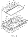
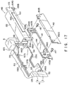
- Fig. 1 shows a portable computer 1 sized to A4.
- the computer 1 comprises a flat box-shaped base unit 2 and a flat panel type display unit 3.
- Housing 4 of the base unit 2 that defines the profile of the base unit 2 is divided into a bottom case 5 having a top opening and a top cover 6 for concealing the top opening of the bottom case 5.
- the bottom case 5 and top cover 6 are formed of a synthetic resin material such as ABS resin.
- the bottom case 5 has a flat bottom wall 5a and a peripheral wall 5b extending from the bottom wall 5a.
- the top cover 6 has a substantially flat top wall 6a and a peripheral wall 6b extending from the top wall 6a.
- the outer surface of the peripheral wall 6b of the top cover 6 is coplanarly aligned with that of the peripheral wall 5b of the bottom case 5 and the peripheral walls 5b and 6b jointly define the front, side and rear ends of the housing 4.
- the top cover 6 is provided on its top wall 6a with a large opening that serves as a keyboard outlet 7, which substantially occupies the entire area of the front half of the top wall 6a.
- the top wall 6a has a projecting portion 8 arranged at its rear end.
- the projecting portion 8 extends between the opposite sides of the top cover 6 and has on its underside and near the opposite ends a pair of grooves serving as stem bearing portions 10a, 10b and a pair of cut off areas 11a, 11b arranged adjacent to the respective stem bearing portions 10a, 10b.
- a keyboard unit 13 is disposed in the front half area of the housing 4.
- the keyboard unit 13 has a keyboard body 14 formed of synthetic resin and having a rectangular plate shape adapted to fit in the keyboard outlet 7.
- the keyboard body 14 has a flat upper surface and a flat lower surface and a number of keys 15 are arranged on the upper surface.
- An aluminum reinforcement plate 17 is laid under the lower surface of the keyboard body 14 with a film 16 inserted therebetween. On the film 16 is printed a circuit pattern in order to transmit switching signals generated by depressing keys.
- the reinforcement plate 17 is rectangular and has a length and a width same with those of the keyboard body 14. The reinforcement plate 17 serves to increase the strength of the keyboard body 14 and, at the same time, prevent switching noises generated by key operations from leaking outside the housing 4.
- the keys 15 of the keyboard unit 13 are exposed through the keyboard outlet 7 of the housing 4, and the reinforcement plate 17 faces inside the housing 4.
- the display unit 3 comprises a thin box-shaped housing 20 and a liquid crystal display 21.
- the housing 20 is divided into a front panel 20a and a rear panel 20b.
- the front panel 20a is provided with a display opening 22, through which the liquid crystal display 21 is exposed.
- the housing 20 is provided at its opposite sides with a pair of horizontal stems 24, 25 projecting therefrom.
- the stem 24 is formed by combining a front stem half 24a integrally formed with the front panel 20a and a rear stem half 24b integrally formed with the rear panel 20b.
- the other stem 25 is also configured in a similar manner.
- the stems 24 and 25 are received by the respective stem bearing portions 10a and 10b and connected to the bottom case 5 of the housing 4 via respective hinges 26.
- Each of the hinges 26 comprises a hinge shaft 27 projecting sideways from the stems 24 or 25.
- the hinge shaft 27 of the hinge 26 for the stem 24 is rigidly held at an end by a bracket (not shown) buried in the stem 24 and connected at the opposite end to another bracket 28, which is rotatable around the axis of the hinge shaft 27, with a wave washer 29 interposed therebetween.
- the wave washer 29 gives rise to frictional resistance between the bracket 28 and the hinge shaft 27 to inhibit free rotation of the hinge shaft 27, and the bracket 28 is inserted into the bottom case 5 from above and rigidly secured to it.
- the above description also applies to the hinge shaft 27 for the stem 25.
- the hinge shafts 27 provide pivots for rotary movement of the display unit 3 so that it may be rotatable to take a first position where it covers the keyboard unit 13, a second position where it stands up behind the keyboard unit 13 to expose the liquid crystal display 21 and a third position where the liquid crystal display 21 is found almost lying flat and opposite to the keyboard unit 13 with respect to the hinge shafts 27.
- the outer surface of the housing 20 of the display unit 3 is coplanarly aligned with that of the housing 4 including the projecting portion 8 to make the computer 1 appear like a flat book that can be conveniently carried by hand.
- the top cover 6 becomes removable from the top of the bottom case 5.
- the hinges 26 are concealed by the projecting portion 8 of the top cover 6 and, if seen from outside, the stems 24, 25 appear to be located in the respective stem bearings 10a, 10b.
- a floppy disc drive (hereinafter referred to as FDD) 30, a hard disc drive (hereinafter referred to as HDD) 40 and a battery pack 50 are arranged in the above mentioned order from right to left in the front half of the bottom case 5 as so may functional components.
- FDD floppy disc drive
- HDD hard disc drive
- battery pack 50 is of modular design and located below the keyboard unit 13.
- the FDD 30 comes in a metal casing 31, which is provided on its front end with an aperture 32 through which a floppy disc can be inserted into and ejected from the casing 31 and a push button 33 that triggers ejection of a floppy disc when it is depressed.
- the casing 31 is also provided on its side ends with respective metal brackets 34a, 34b having respective lugs 35a, 35b, 36a, 36b extending upward from the top of the casing 31.
- the FDD 30 is disposed on the bottom wall 5a with the aperture 32 and the push button 33 facing the front end of the bottom case 5 and exposed to the outside through an access opening 37 cut through the front wall of the bottom case 5 near its right side end.
- the HDD 40 also comes in a metal housing 41 that contains magnetic discs and heads hermetically sealed therein.
- a circuit board 42 is arranged on the top of the housing 41 and various circuit components are mounted on the circuit board 42 to form a control circuit and a drive circuit for the HDD 40.
- the housing 41 is arranged on the bottom wall 5a side by side with the FDD 30 and carries on its lateral wall a metal bracket 44, which by turn comprises a pair of fixtures 45a, 45b that are rigidly secured to respective upright bosses 47, 47 projecting from the bottom wall 5a by means of screws 46, 46.
- the battery pack 50 is rechargeable and serves as power source when the computer 1 is used without any commercial power supply.
- the battery pack 50 has a flat and rectangular synthetic resin case 51, which contains therein a plurality of rechargeable batteries and is arranged on the bottom wall 5a of the bottom case 5.
- the bottom wall 5a of the bottom case 5 carries thereon a pair of guide walls 52a, 52a standing there to guide the sides of the case 51 and defining a batter storage section 53 within the bottom case 5.
- the battery storage section 53 is located to the left of the bottom case 5 and accessible through a battery insertion opening 54 cut through the front wall of the bottom case 5 near its left side end.
- a battery pack 50 may be inserted into and ejected from the battery storage section 53 through the insertion opening on the front side of the housing 4.
- the battery access opening 54 includes a bottom opening 54a cut through the bottom wall 5a of the bottom case 5.
- the front edge of the bottom wall 5a defining the rear end of the bottom opening 54a is found behind the front wall of the bottom case 5.
- the case 51 of the battery pack 50 has a downward ridge 55 extending along the front end and between the opposite side ends of the case 51.
- the downward ridge 55 makes part of the bottom wall 5a of the bottom case 5 when the battery pack 50 is inserted into the battery storage section 53 and serves as a hook for receiving a finger tip when the battery pack 50 is pulled out of the battery storage section 53.
- the battery storage section 53 is provided along its rear end with a pair of upwardly projecting stoppers 56a, 56b. As a battery pack 50 is inserted into the battery storage section 53, its front end eventually abuts the stoppers 56a, 56b so that the battery pack 50 is held in position within the battery storage section 53.
- the case 51 is provided along its front end with positive and negative power supply terminals 57a, 57b connected to the batteries housed in the case 51 and a pair of connector terminals 58a, 58b connected to a safety fuse and a temperature sensor (not shown).
- a board unit 60 that operates as one of functional components is housed in the rear half of the bottom case 5 and located behind the FDD 30, the HDD 40 and the battery pack 50 as it extends all the way between the opposite side ends of the bottom case 5.
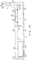
- the board unit 60 of the embodiment comprises, as shown in Figs. 9 and 11, first through fifth circuit boards 61a through 61e and a shield frame 62 holding and surrounding the circuit boards 61a through 61e arranged in mutually separated three layers laid along the height of the housing 4.
- the circuit boards 61a through 61e are prepared by cutting a single rigid board base and have appropriate respective dimensions. Each of the boards carries on its upper and lower surfaces given circuit patterns (not shown) formed by printing. As shown in Fig. 11, the circuit boards 61a through 61e are divided into two groups. The first through third circuit boards 61a through 61c are arranged on a side by side basis along the transversal direction of the bottom case 5 to form a first board group 63, while the fourth and fifth circuit boards 61d and 61e are arranged in a similar manner to form a second board group 64.
- the first circuit board 61a and the second circuit board 61b are electrically connected with each other via a first flexible connecting board 65a, whereas the first circuit board 61a and the third circuit boards 61c are electrically connected with each other via a second flexible connecting board 65b.
- the fourth circuit board 61d and the fifth circuit board 61e are electrically connected with each other via a third flexible connecting board 65c, whereas the first circuit board 61 and the fourth circuit board 61d are electrically connected with each other via a fourth flexible connecting board 65d.
- the circuit boards 61a through 61e are separated from one another, they are electrically mutually connected.
- the circuit boards 61a through 61e carries on their upper and lower surfaces a number of circuit components 66, which are connected to the respective circuit patterns.
- the circuit components 66 include those that generate and emit high frequency noises as well as heat.
- the third circuit board 61c in this embodiment constitutes a power supply board, most of the circuit components arranged on it can generate heat at a considerable rate.
- the shield frame 62 comprises a first shield plate 68, a second shield plate 69 and a connector board 70 disposed between the shield plates 68 and 69.
- Each of the shield plates 68 and 69 and the connector board 70 is made of a metal plate having an electromagnetic shield effect.
- the first shield plate 68 comprises as integral parts thereof an oblong base plate section 71 to be directly placed on the bottom wall 5a of the bottom case 5 and an upright section 72 standing from some of the edges of the base plate section 71.
- the base plate section 71 is provided with first support portions 73 for supporting the first circuit board 61a, second support portions 74 for supporting the second circuit board 61b and third support portions 75 for supporting the third circuit board 61c.
- These support portions 73, 74 and 75 are formed by partly cutting the base plate section 71 to produce curved slits and bending the cut areas upward along the lines connecting the opposite ends of the respective slits.
- the first and second support portions 73 and 74 have a substantially equal height, whereas the third support portions 75 is higher than the other two support portions 73 and 74.
- the first and second circuit boards 61a and 61b are supported respectively by the front ends of the first and second support portions 73 and 74 and secured thereto by means of screws.
- the base plate section 71 covers the undersides of the first and second circuit boards 61a and 61h and some of the circuit components 66 are arranged between the base plate section 71 and the circuit board 61a or 61b.
- the second connecting board 65b connecting the first circuit board 61a and the third circuit board 61c is bent to show a turned U-shaped cross section so that the third circuit board 61c may be located above the first and second circuit boards 61a and 61b.
- the third circuit board 61c is supported by the front end of the third support portions 65b and secured thereto by means of a screw at an end opposite to the end where it is connected to the connector board 65b.
- the three circuit boards 61a through 61c are arranged on the first shield plate 68 in two layers.
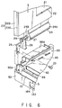
- the base plate section 71 of the first shield plate 68 has a right side extension 71a extending from the side of the base plate section 71 located opposing to the second circuit board 61b.
- the extension 70a is found behind the FDD 30 and covered by a metal plate cover 80 as illustrated in Fig. 10.
- the cover 80 comprises a partition 81 disposed above the extension 71a and lugs 82 arranged on the four corners of the cover 80.
- the lugs 82 are respectively placed on the corners of the extension 71a and the front ends of the second support portions 74 and secured thereto by means of screws 83.
- the second shield plate 69 comprises as integral parts thereof an oblong base plate section 85 transversally extending on the housing 4 and an upright section 86 standing from an edge of the base plate section 85.
- the base plate section 85 is provided with first support portions 87 for supporting the fourth circuit board 61d and second support portions 88 for supporting the fifth circuit board 61e.
- the fourth circuit board 61d and the fifth circuit board 61e are respectively secured to the front ends of the first support portions 87 and the front ends of the second support portions 88 by means of screws.
- the circuit boards 61a through 61e are respectively secured to the first and second shield plates 68 and 69, the shield plates 68 and 69 are connected to each other via the fourth connecting board 65d. Then, the shield plates 68 and 69 are put together on a one on the other basis, i.e., superposed with each other, the fourth connecting board 65d being bent to show a turned U-shaped cross section. Under this condition, the shield plates 68 and 69 are rigidly secure to each other by means of screws (not shown).
- the base plate section 71 of the shield plate 68 and the base plate section 85 of the shield plate 69 are oppositely located and the circuit boards 61d and 61d secured to the base plate section 85 are located above the circuit boards 61a through 61c arranged on the base plate section 71.
- the circuit boards 61a through 61e are arranged in three layers in the housing 4.
- the third circuit board 61c dedicated to power supply and hence apt to emit heat at an enhanced rate is disposed between the first circuit board 61a and the fourth circuit board 61d.
- the upright sections 72 and 86 are arranged side by side to provide the left side wall and the rear wall of the shield frame 62.
- the upright sections 72 and 86 are provided with a plurality of connector access apertures 92 that allows lead wires of various connectors to pass therethrough.
- the connecting board 70 is disposed between front end of the base plate section 71 and that of the base plate section 85 and secured to the base plate sections 71 and 85 by means of screws.
- the connecting board 70 provides the front wall of the shield frame 62 and the fourth circuit board 61d is partly supported on the top of the connecting board 70.
- Near the left side end of the connecting board 70 there is formed an slot 94 through which the front end of the battery pack 50 is introduced.
- the battery pack 50 is held under an area of the base plate section 85 located above the slot 94.
- the board unit 60 comprising the circuit boards 61a through 61e and the shield frame 62 is loaded on the bottom wall 5a of the bottom case 5. Then, as shown in Figs. 3 and 4, lugs 95a extending from the connecting board 70 and a lug 95b arranged at the front right corner of the second shield plate 69 are fitted to respective bosses 46 erected on the bottom wall 5a of the bottom case 5 by means of screws. Note that the lug 95b is secured to the corresponding boss 46 as it is placed on the case 31 of the FDD 30, whereas the lugs 95a are respectively secured to the bosses 46 with anchoring members 46b of the HDD 40.
- anchoring members 96a and 96b are formed at the respective ends of the upright sections 72 and 86 that provide rear wall for the shield frame 62 and the brackets 28 of the hinges 26 are respectively secured to the anchoring members 96a and 96b by means of screws.
- the shield frame 62 is designed to support the display unit 3 too.
- a pair of synthetic resin covers 98a, 98b are secured to respective rear end areas of the upper surface of the shield frame 62. These covers 98a, 98b are so designed as to conceal the openings of the stem bearing portions 10a, 10b from under when the top cover 6 is fitted onto the bottom case 5 and provide bottoms for the respective stem bearing portions 10a, 10b.
- the fourth circuit board 61d located on the top layer is provided with a spare zone 101 for receiving thereon one or more than one additional circuit components 100 such as a keyboard controller to be installed in order to upgrade the portable computer.
- the spare zone 101 is located at the middle of the board unit 60 in the longitudinal direction of the unit 60 and will be filled with circuit patterns.
- the base plate section 85 of the second shield plate 69 that covers the fourth circuit board 61d from above is provided with a cut out area 102 at a position facing at least the spare zone 101 and most of the upper surface of the fourth circuit board 61d including the spare zone 101 is upwardly exposed through the cut out area 102.
- the shield plate 105 comprises, as illustrated in Figs. 2 through 4 and 12, a flat and rectangular main section 105a realized in a form that corresponds to the plan view of the front half of the bottom case 5.
- the main section 105a is provided along its edges with a plurality of lugs 106.
- the shield plate 105 is then secured to the lugs 35a, 35b, 36a, 36b, while the lugs 106 are secured by screws 47 to the corresponding bosses 46 on the bottom wall 5a of the bottom case 5.
- lugs 106 those arranged at the rear corners of the main section 105a are laid on the respective lugs 95a, 95b of the shield frame 62 on the bosses 46 so that the shield frame 62 and the shield plate 105 are electrically connected with each other.
- the main section 105a of the shield plate 105 is located below the keyboard unit 13, and the reinforcement plate 17 of the keyboard unit 13 is located opposing to the shield plate 105 with a narrow clearance therebetween.
- a pair of metal plate springs 107a and 107b are arranged near the respective side edges and on the upper surface of the shield plate 105.
- Each of the plate springs 107, 107b are equipped with a plurality of resiliently deformable contact pieces 108, which are held in contact with the reinforcement plate 17 of the keyboard unit 13 so that the shield plate 105 and the reinforcement plate 17 are electrically connected with each other.
- the shield plate 105 has as integral part thereof an extension 110 extending from the rear end of the main section 105a toward the board unit 60.
- the extension 110 has a shape corresponding to that of the cut out area 102 and covers the cut out area 102 and the fourth circuit board 61d that carries thereon the spare zone 101.
- the extension 110 has at its front end a connecting portion 111 as integral part thereof, and the connecting portion 111 is secured to the rear end of the shield frame 62 by means of screws. Thus, the extension 110 may not lift unintentionally, and the board unit 60 is held between the extension 110 and the bottom wall 5a of the bottom case 5.
- the extension 110 is located close to the rear half of the top wall 6a of the top cover 6 and has a transversely extending recess 112 for receiving a reflection type liquid crystal display 113, which is designed to display various operating conditions of the computer 1.
- the liquid crystal display 113 has an oblong rectangular plan view. While it is held immovable relative to the recess 112 in the transverse direction of the housing 4, its position is adjustable forwardly or rearwardly within a given limit.
- the recess 112 has a width slightly greater than that of the liquid crystal display, and oppositely arranged pairs of engaging members 114a, 114b and 115a, 115b are projecting toward the corresponding ones from the front and rear edges of the recess.
- the front and rear sides of the liquid crystal display 113 are separated from the respective engaging members 114a, 114b and 115a, 115b by narrow clearances 116 so that the liquid crystal display 113 may be shifted forwardly or backwardly within the limit.
- the top surface of the liquid crystal display 113 is found above the upper surface of the extension 110.
- An oblong display window 117 is formed through the rear half of the top wall 6a of the top cover 6 to expose the liquid crystal display 113.
- a transparent protective cover 118 is fitted to the display window 117.
- the top wall 6a has as integral part thereof on its inner surface with downwardly projecting ridges 120a and 120b extending respectively along the front and rear edges of the display window 117. As shown in Fig. 13, the ridges 120a and 120b are respectively located right above the upper front edge and the upper rear edge of the liquid crystal display 113 and oppositely chamfered to produce guide bevels 121a and 121b that provide a greater distance therebetween toward the ridgelines.
- the guide bevels 121a and 121b are so arranged that they respectively abut the upper front edge and the upper rear edge of the liquid crystal display 113 when the top cover 6 is properly put on the bottom case 5.
- the liquid crystal display 113 is moved forward or rearward as a function of the inclination of the guide bevels 121a and 121b to offset any clearances between the display window 117 of the top cover 6 and the liquid crystal display 113.
- the liquid crystal display 113 is pressed against the bottom of the recess 112 so that the display 113 may not be allowed to accidentally tilt in any directions.
- the board unit 60 is provided at its right side with first and second card slots (card storage spaces) 125 and 126 for receiving function expansion cards.
- the card slots 125 and 126 are arranged on a one above the other basis.
- the lower first card slot 125 is formed between the extension 71a of the first shield plate 68 and the partition 81 of the cover 80 to dimensions typically capable of storing any card conforming to the applicable PCMICA standard including those for thick type cards that may have a maximum thickness of 18.0 mm.
- This first card slot 125 is designed to typically receive a card, such as an expansion card 127, which may be constantly used and is held in the slot without being frequently drawn out the slot. As may be understood from Fig.
- the second circuit board 61b is located near an end of the first card slot 125 and a connector 300 conforming to the PCMCIA standard is arranged on the second circuit board 61b.
- the connector 300 is designed to be connected to a terminal section 127a of the expansion card 127, whereas the terminals of the connector 300 are connected to the circuit pattern formed on the circuit board 61b.
- the second card slot 126 is formed between the partition 81 of the cover 80 and the base plate section 85 of the second shield plate 69 and extension 110 of the shield plate 105 disposed adjacent to the base plate section 85.
- the second card slot 126 is formed to dimensions appropriate to receive a card of type 1 with a thickness of 3.3 mm or of type 2 with a thickness of 5.0 mm, e.g., an interface card 128, which may be frequently inserted and drawn out the card slot 126.
- the interface card 128 normally has terminal sections 129a and 129b arranged at opposite ends thereof and a thickness smaller than that of the expansion card 127. As may be seen from Fig.
- the fifth circuit board 61e is located close to an end of the second card slot 126, and a connector 302 conforming to the applicable PCMCIA standard is arranged on the fifth circuit board 61e.
- the connector 302 is designed to be connected to the terminal section 129a of the interface card 128, whereas the terminals of the connector 302 are connected to the circuit pattern formed on the circuit board 61e.
- side walls of the cover 80 defining the first card slot 125 have respective outwardly projecting lower end portions that define a pair of guide grooves 303 for guiding the side edges of the card 127.
- Each of the lower end portions of the cover 80 is provided with a pair of projections 304 formed by pressing parts of the lower end portions. These projections 304 project into the respective guide grooves 303 and abut the respective side edges of the card inserted into the first card slot 125 to hold the card in position.
- a total of four projections 306 are formed on the extension 71a of the first shield plate 68 in a manner as described above with regard to the projections 304. The projections 306 are designed to abut the lower surface of the card inserted into the first card slot 125 to hold the card in position.
- the partition 81 of the cover 80 that defines the second card slot 126 is provided with four projections 308 that are designed to abut the lower surface of the card inserted into the second card slot 126 to hold the card in position. Additionally, a pair of guides (not shown) are arranged in the second card slot 126 to guide the side edges of the card.
- the first card slot 125 and the second card slot 126 have an identical width. In other words, the distance between the guide grooves 303 for the first card slot 125 and the distance between the guides for the second card slot 126 are equal to each other.
- the card slots 125 and 126 differs from each other only in terms of height.
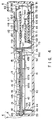
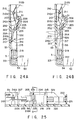
- Fig. 15 illustrates cards conforming to the PCMCIA standard and usable in either the first card slot 125 or the second card slot 126. More specifically, a thick type card 127 as illustrated in Figs. 10 and 15 is substantially rectangularly parallelepipedic and provided with guide ribs 310 projecting from lower portions of the respective side walls.
- the card 127 has a thickness DT of 18.0 mm and each of the guide ribs has a thickness D1 of 3.3 mm, whereas the lower ends of the guide ribs are spaced from the bottom of the card by a distance Y of 0.85 mm, and the card has an overall width W1 of 54.0 mm including the guide ribs and has a width W2 of 51.0 mm without the guide ribs.
- the type 3 card has a thickness D3 of 10.5 mm which is smaller than the thickness of the thick type card but is identical with the thick type card 127 in any other dimensions.
- the type 2 card has a thickness D2 of 5.0 mm and a width W2 of 48.0 mm but is identical with the thick type card 127 in any other respects.
- the type 1 card has a thickness D1 of 3.3 mm and a distance Y of 0 mm between the lower ends of the guide ribs and the bottom of the card but identical with the cards of the type 2 in any other respects.
- each card is provided with a terminal section (127a, 129a or 129b) conforming to the PCMCIA standard, which is to be connected to the connector 300 or 302 arranged in the card slot 125 or 126.
- the guide ribs 310 of the cards of any types has common dimensions, and each card is inserted into the first or second card slot 125 or 126 while the guide ribs 310 are guided by the guide grooves 303 or the guides of the card slots.
- the first card slot 125 can selectively receive any one of the cards of any types
- the second card slot 126 can electively stores one of cards of type 1 and type 2 which are normally designed to be frequently loaded and unloaded.
- Fig. 16 illustrates the control system for controlling the cards loaded in the first and second card slots 125 and 126.
- the card loaded in the first card slot 125 typically an I/O card 127
- the card loaded in the second card slot 125 is connected to the card controller 323 via the connector 302.
- the card controller 323 is controlled by a socket service 324 and a card service 325 of a BIOS-ROM.
- the card controller 323 is then connected to the internal bus of the computer to specify an address space to be used to access the cards 127 and 128, control read/write operations and detect card insertions and ejections.
- the socket service 324 basically has basic function required to control hardware and is capable of coordinating the cards 125 and 126, the card controller 323 and other pieces of hardware of different functional levels.
- the card service 325 defines the application software interface required to access the cards 125 and 126 from a given application program by using OS (operating system) 326.
- the computer is equipped with the first card slot 125 capable of storing the thick type card, and the second card slot 126 for receiving a thin card of type 1 or type 2.
- the computer can be operated while two cards are simultaneously stored in the first and second card slots 125 and 125, for example, while the first card slot stores a selected type of card, e.g., an I/O card and the second card slot stores a card such as a security card which is frequently inserted and ejected from the slot.
- the computer can be obtained a high expansion capability.
- the housing 4 has in its rear half an opening 135 that communicates with the first and second card slots 125 and 126.
- the opening 135 specifically comprises a side opening 135a formed through the right side wall of the housing 4, a top opening 135b arranged through the top wall 6a of the top cover 6 and extending from the side opening 135a, and a bottom opening 135c cut through the bottom wall 5a of the bottom case 5 and also extending from the side opening 135a.
- a flat receiving portion 136 is horizontally extending from and located adjacent to the edge of the top wall 6a that defines an end of the top opening 135b.
- a cover 140 is fitted to the housing 4 to cover the opening 135.
- the cover 140 comprises a cover support 141 to be rigidly fitted to the bottom case 5 of the housing 4, a first cover member 142 removably fitted to the cover support 141, and a second cover member 143 fitted to the cover support 141 and rotatable between an opened position and a closed position.
- the cover support 141 includes a flat fitting portion 144 to be received in the bottom opening 135c, and a pair of vertical support walls 145a, 145b extending from the fitting portion 144 and fitted into the side opening 135a.
- the support walls 145a, 145b are separated from each other in the depth direction of the housing 4 and located in the side opening 135a.
- These support walls 145a, 145 are rigidly fitted to respective bosses 146a, 146b of the bottom case 5 by means of screws 147 and have a height substantially equal to that of the side wall 5b of the bottom case 5.
- the support walls 145a, 145b are respectively provided with engaging holes 148a, 148b and pivots 149a, 149b.
- the first cover member 142 is used to selectively conceal and expose the first card slot 125 and is formed as an oblong flat plate extending between the support walls 145a and 145b.
- the first cover member 142 is designed to conceal the lower half of the side opening 135a and provided with a pair of engaging projections 150a, 150b at locations facing the support walls 145a, 145b.
- the first cover member 142 is fitted to the cover support 141 to cover the first card slot 125 from the outside when the engaging projections 150a, 150b are releasably engaged with respective engaging holes 148a, 148b formed in the support walls 145a, 15b. Under this condition, the outer surface of the first cover member 142 is flush with that of the side wall 5b of the bottom case 5 and constitutes part of the side wall 5b.
- the second cover member 143 is designed to selectively conceal the second card slot 126 and comprises a top wall section 152 for closing the top opening 135b and a side wall section 153 extending from the top wall section 152 to close the upper half of the side opening 135a.
- Both the top wall section 152 and the side wall section 153 have a flat and oblong form extending in the depth direction of the housing 4.
- the side wall section 153 is provided with a pair of legs 154a, 154b downwardly extending from its front and rear ends respectively. The legs 154a, 154b are used to hold the vertical walls 145a, 145b of the cover support 141 from the front side and the rear side respectively.
- the legs 154a, 154b are provided with respective bores 155a, 155b for rotatably receiving the respective pivots 149a, 149b.
- the upper surface of the top wall section 152 is coplanar with the upper surface of the top wall 6a of the top cover 6 and, at the same time, the outer surface of the side wall section 153 is also coplanar with the outer surface of the side wall 6b of the top cover 6 to appear as if an integral part of the top cover 6. Under this condition, the top wall section 152 is located on the receiving portion 136 within the top opening 135b to suppress any upward displacement of the top cover 6.
- anchoring projections 156, 156 arranged along the front edge of the top wall section 152 are engaged with respective hooks 157a, 157b projecting from the corresponding edge of the top wall 6a to hold the second cover member 143 in the closed position as may be seen from Fig. 14.
- the side wall section 153 of the second cover member 143 is provided with a terminal access opening 160 leading to the second card slot 126.
- the terminal access opening 160 extends in the depth direction of the housing 4 and is opposite to the terminal section 129b of the interface card 128 in the second card slot 126.
- a lid plate 161 for opening and closing the terminal access opening 160 is fitted to the side wall section 153. It is made of a plate, having an oblong front view corresponding to that of the terminal access opening 160, and provided with a pair of pivots 162 and a pair of anchoring projections 163 arranged lengthwise near the respective side ends (only one of the pivots and one of the anchoring projections are shown in Fig. 14).
- the pivots 162 are rotatably held at the respective edges of the side wall section 153 defining the terminal access opening 160 so that the lid plate 161 may be rotatable around the pivots 162 between a closed position where it covers the terminal access opening 160 and an opened position where it gets to expose the terminal access opening 160 as it is rotated counterclockwise.
- the anchoring projections 163 are engaged with the edge of the side wall section 153 defining the terminal access opening 160 to hold the lid plate 161 in the closed position.
- the outer surface of the lid plate 161 is coplanar with the outer surface of the side wall section 153 of the cover member 142, thereby constituting part of the side wall section 153.
- the cover 140 having a configuration as described above, when the lid plate 161 is opened while the interface card 128 is loaded in the second card slot 126 as illustrated in Fig. 14, the terminal section 129b of the interface card 128 is exposed to the outside through the terminal access opening 160 so that the connector of an external expansion device may be connected to the terminal section 129b without opening the second cover member 143.
- the board unit 60 is provided at its left end with a third card slot 131 disposed between the fifth circuit board 61e and the base plate section 85 of the second shield plate 69.
- This third card slot 131 is provided with a card insertion port 133 cut through the left side wall of the shield frame 62.
- the third card slot 131 is designed to receive another expansion card 132 through the card insertion port 133.
- a connector (not shown) to be connected to the card 132 is arranged on the fifth circuit board 61e.
- a card inserting slot 170 is cut through the rear half of the left side wall of the housing 4, leading to the third card slot 131. More specifically, the card inserting slot 170 is formed in the side wall 6b of the top cover 6 and extends in the depth direction of the housing 4.
- the side wall 6b of the top cover 6 is provided with a lid plate 171 for closing and opening the card inserting slot 170.
- the lid plate 171 has an oblong front view conforming to that of the card inserting slot 170 and is provided at its front and rear ends with a pair of pivots 172 and a pair of anchoring projections 173 (only one of the pivots and one of the projections are shown in Figs. 19 and 20).
- the pivots 172 are rotatably held at the respective edges of the side wall 6b defining the card inserting slot 170 so that the lid plate 171 is rotatable around the pivots 172 between a closed position where it covers the card inserting slot 170 and an opened position where it gets to open the card inserting slot 170 as it is rotated lift side.
- the anchoring projections 173 are engaged with the respective edges of the side wall 6b defining the card inserting slot 170 to hold the lid plate 171 to the closed position.
- the outer surface of the lid plate 171 is coplanar with the outer surface of the side wall 6b of the top cover 6 and constitutes part of the side wall 6b.
- the board unit 60 is provided with a power switch 180 at its left side end.
- the power switch 180 comprises a depressible actuator 181 projecting through the left side wall of the shield frame 62, or the upright section 72 of the first shield plate 68, toward the side wall 5b of the bottom case 5.
- a synthetic resin control button 182 to be used for turning on and off the power switch 180 is arranged on the side wall 5b of the bottom case 5. As illustrated in Figs. 21 and 22, the control button 182 has a rectangular push pad 183 to be depressed by a finger tip of the operator. The pad 183 is exposed from the left side of the bottom case 5 through a hole 184 cut through the side wall 5b.
- a pair of stopper walls 185a, 185b are arranged to the opposite lateral sides of the pad 183 so that, once the pad is set in position, they project toward the upright section 72 of the first shield plate 68.
- the stopper walls 185a, 185b are provided as integral part thereof with respective support members 186a, 186b extending downward.
- the lower ends of the support members 186a, 186b are mutually connected by a flat and oblong coupling portion 187.
- the support members 186a, 186b and the coupling portion 187 are resiliently deformable.
- the coupling portion 187 is located below the pad 183 and placed on the bottom wall 5a of the bottom case 5.
- a pair of support walls 189a, 189b are formed on the bottom wall 5a of the bottom case 5 and located under the hole 184.
- the support walls 189a, 189b are provided on the upper edges with grooves 190, 190 into which the coupling portion of the control button 182 is fitted.
- the control button 182 is held on the bottom wall 5a of the bottom case 5 by way of the coupling portion 187 so that the pad 183 is held the hole 184 with being in parallel to the side wall 5b by means of the resilient force of the coupling portion 183 and the support members 186a, 186b.
- the coupling portion 187 is deformed along with the support members 186a, 187 until the pad 183 is pushed into the bottom case 5 and the stopper walls 185a, 185b abut the upright section 72.
- the stroke of movement of the pad 183 is defined by the stopper walls 185a, 185b.
- the push pad 183 has on its lower end of the back side a pusher lug 191 extending upward as integral part thereof.
- the pusher lug 191 is resiliently deformable to move toward and away from the pad 183, and its fee upper end is held in contact with the actuator 181.
- the actuator 181 is pushed back by the pusher lug 191 to turn on or off the power switch 180.
- the push pad 183 can be depressed until the stopper walls 185a, 185b abut the shield frame 62. Since the resiliently deformable pusher lug 191 is disposed between the pad 183 and the actuator 181, even when the stroke of the pad 183 is increased due to deformation of the stopper walls 185a, 185b and the like, any excessive stroke of the pad 183 can be absorbed by the elastic deformation of the pusher lug 191. Thus, as the push button 182 is pushed, the actuator 181 can be prevented from being subjected to excessive load, thereby preventing damage or otherwise trouble of the power switch 180.
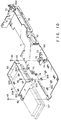
- the bottom case 5 contains in the left end of the front half a lock mechanism 200 for manually releasably locking a battery pack 50 in the battery storage section 53.
- the lock mechanism 200 comprises a lock lever 201 for releasably engaging the case 51 of the battery pack 50.
- the lock lever 201 is located between the left side portion of the peripheral wall 5b of the bottom case 5 and the left side guide wall 52a.
- the lock lever 201 comprises, as illustrated in Fig. 27, a cylindrical boss 202, an engaging arm 203 extending from the outer periphery of the boss 202, and an pressing arm 204 also extending from the outer periphery of the boss 202 in a direction opposite to that of the engaging arm 203.
- the boss 202 is rotatably supported by a pivot 205 standing on the bottom wall 5b of the bottom case 5 so that the engaging arm 203 and the pressing arm 204 are rotatable around the pivot 205.
- the left side guide wall 52a has, as illustrated in Fig. 7, a notched portion 207 opening to the battery storage section 53.
- the notched portion 207 is located to oppose the engaging arm 201 of the lock lever 201 so that the engaging arm 203 and the corresponding side of the case 51 come to face each other through the notched portion 207.
- the case 51 of the battery pack 50 is provided on its side wall with an engaging recess 208 which faces the notched portion 207 when the battery pack 50 is properly loaded into the battery storage section 53. Then, the engaging recess 208 is located opposing to an engaging tip 209 formed on the free end of the engaging arm 203.
- a torsion coil spring 210 as a first spring is arranged behind the lock lever 201.
- the torsion coil spring 210 comprises a coiled section 210a supported on a support pillar 211 standing on the bottom wall 5a, and a pair of arms 210b, 210c extending from the coil section 210a.
- the free end of the arm 210b is anchored to the bottom case 5 whereas the free end of the arm 210c is hooked on the engaging arm 203.
- the lock lever 201 is urged by the spring 210 to rotate clockwise so that engaging tip 207 of the engaging arm 203 faces the notched portion 207 and projects into the battery storage section 53.
- the engaging tip 207 comes to engage with the engaging recess 208, thereby locking the battery pack 50 in the battery storage section 53.
- the bottom case 5 is provided on the left side portion of the peripheral wall with a window 213 through which a finger tip may go through upon releasing the lock.
- the window 213 is located to face the pressing arm 204 of the lock lever 201.
- the lock lever 201 is rotated counterclockwise against the urging force of the torsion coil spring 210.
- the engaging tip 209 is disengaged from the engaging recess 208 to release the battery pack 50 out of the locked condition.
- the lock mechanism 200 additionally comprises a shutter 215 for selectively closing and opening the window 213.
- the shutter 215 is located in front of the lock lever 201 and between the left side guide wall 52a and the peripheral wall 5b of the bottom case 5.
- the shutter 215 comprises a side wall section 216 extending along the inner surface of the peripheral wall 5b of the bottom case 5, a top wall section 217 extending horizontally from the upper end of the side wall section 216 toward the guide wall 52a, and a front wall section 218 connecting the front end of the top wall section 217 and that of the side wall section 216.
- the lower end of the side wall section 216 is slidably fitted in a guide groove 220 formed on the bottom wall 5a of the bottom case 5 and extending in the depth direction of the housing 4.
- the top wall section 217 and the front wall section 218 are slidably in contact with the guide wall 52a.
- the shutter 215 is slidable between a closed position where it is located between the window and the pressing arm 204 of the lock lever 201 to close the window and an opened position where it opens the window 213 to expose the pressing arm 204 of the lock lever 201.
- a compression coil spring 222 under a compressed condition between the front wall section 218 of the shutter 215 and a spring holder 221 disposed at the front end of the bottom case 5 so that the shutter 215 is constantly urged toward its closed position where it closes the window 213.
- the pressing arm 204 of the lock lever 201 is found inside the side wall section 216 of the shutter 215 and constantly pressed against the inner surface of the side wall section 216, as illustrated in Fig. 23.
- the side wall section 216 of the shutter 215 leaves the pressing arm 204 to make the latter exposed to the outside through the window 213.
- the lock lever 201 is rotated clockwise by an angle corresponding to the thickness of the side wall section 216 as it is urged to rotate by the torsion coil spring 210. Consequently, the front end of the pressing arm 204 comes to face the front edge 216a of the side wall section 216.
- the front end of the pressing arm 204 is hooked by the front end of the pressing arm 204 as the shutter moves toward the closed position by the urging force of the compression coil spring 222, so that the shutter 215 is held to its opened position against the urging force of the compression coil spring 222.
- the side wall section 216 is provided with a finger tip receiving rib 223 facing the window 213.
- the bottom case 5 is equipped on its right side of the front half with an expansion connector 231 to which a track ball 230 is to be connected.
- a track ball 230 is one of pointing devices used for specifying a particular position on the screen of the liquid crystal display 21 and, as shown in Fig. 32, provided with a spherical control section 233 on the upper surface of its main body case 232. An operator can shift the cursor position in the display screen and perform other operations by appropriately rotating the control section 233 with a finger tip.
- the main body case 232 is provided at its one end with a connector 235 that may be removably fitted to the expansion connector 231.
- the connector 235 comprises a synthetic resin connector body 236 having a pair of engaging projections 236a, 236b and a pair of contact terminals 237, 237 arranged between the engaging projections 236a, 236b.
- the expansion connector 231 of the bottom case 5 is provided with a synthetic resin connector body 240.
- the connector body 240 is formed of an elongated box extending lengthwise in the bottom case 5, and is integrally provided with a pair of flanges 241a, 241b extending from the opposite longitudinal ends.
- the connector body 240 is arranged along the right side portion of the peripheral wall 5b of the bottom case 5 with the flanges 241a, 241b rigidly secured to a pair of respective bosses 242a, 242b projecting upward from the bottom wall 5a by means of screws 243.
- the connector body 240 is located to the right of the FDD 30.
- the connector body 240 is also provided with a pair of engaging recesses 244 to which the engaging projections 36a, 36b of the connector 235 are removably fitted.
- the recesses 244 are arranged opposing the right side portion of the peripheral wall 5b of the bottom case 5.
- a pair of terminal plates 245 are arranged between the engaging recess 244 to establish electric connection with the respective contact terminals 237, 237.
- the terminal plates 245 are electrically connected to the board unit 60 through a flexible connecting board 246.
- the engaging recesses 244 and the connector plates 245 of the connector body 240 are exposed to the outside through an elongated connector access opening 248 formed in the peripheral wall 5b of the bottom case 5.
- the connector body 240 is molded with a metal conductor plate 250 as integral part thereof.
- the conductor plate 250 has a first exposed area 251 connecting the tops and the bottoms of the engaging recesses 244 and a pair of second exposed areas 252 extending from the first exposed area 251 and arranged on the rear surface of the connector body 240. As shown in Fig. 29, the first exposed area 251 extends closer to the outer extremities of the engaging recesses 244 than the terminal plates 245 and also to above and below the terminal plates 245, 245.
- the second exposed areas 252 are provided with respective grounding terminals 255a 255b.
- one of the grounding terminals, or the terminal 255a is laid under the lower surface of the front flange 241a, whereas the other grounding terminal 255b is laid on the upper surface of the rear flange 241b.
- a grounding metal fitting 256 is interposed between the grounding terminal 255a and the boss 242a and secured to the boss 242a by means of a screw 243.
- a grounding metal fitting 256 has as integral part thereof a conductive member 257, which conductive member 257 is secured onto the lug 36b by means of a screw 258 and receives thereon the shield plate 105.
- conductor plate 250 of the connector body 240 is electrically connected to the casing 31 and the shield plate 105 via the grounding terminal 255a and the grounding metal fitting 256.
- the electrostatic charge that may have been accumulated on the contact terminals 237 and/or the terminal plates 245 can be discharged therebetween when the connector 235 of the track ball 230 is connected to the expansion connector 231.
- the expansion connector 231 is molded as integral part thereof with the conductor plate 250 having the first exposed area 251 extending closer to the outer extremities of the engaging recesses 244 than the terminal plates 245 and also to above and below the terminal plates 245, the first exposed area 251 approaches the contact terminals 237 before it approaches the terminal plates 245 when the two connectors are put together so that any accumulated electrostatic charge may be discharged firstly between the first exposed area 251 and the contact terminals 237. Because the conductor plate 250 is electrically connected to the casing 31 of the FDD 30 via the grounding metal fitting 256, the electrostatic charge will be safely led to the casing 31 of the FDD 30 and then to the shield plate 105 for discharging.
- the bottom case 5 is provided with a shutter plate 260 for selectively closing and opening the connector access opening 248.
- the shutter plate 260 has a rectangular plan view that corresponds to that of the connector access opening 248 and slidable lengthwise along the right side portion of the peripheral wall 5b of the bottom case 5 between a closed position where it covers the connector access opening 248 and an opened position where it exposes the connector access opening 248 and hence the engaging recesses 244 of the connector body 240.
- a guide wall 261 is arranged on the bottom wall 5a of the bottom case 5 to slidably hold the shutter plate 260 between the peripheral wall 5b of the bottom case 5 and itself.
- the guide wail 261 is located behind the connector body 240 and has a flat wall section 262 extending forward from the front end of the guide wall 261 and between the connector body 240 and the peripheral wall 5b.
- the wall section 262 is designed to hold the shutter plate 260 between the peripheral wall 5b and itself. Therefore, it may be understood that the expansion connector 231 operates also as a guide wall for guiding the sliding movement of the shutter plate 260.
- the shutter plate 260 is equipped with a rib 263 for receiving a finger tip coming into the connector access opening 248.
- an FDD 30, an HDD 40, a battery pack 50 and a board unit 60 are placed on the respective proper positions on the bottom wall 5a of the bottom case 5. Then, the lug 95b extending from the connecting board 70 of the shield frame 62 is laid on the upper surface of the metal casing 31 of the FDD 30 and the slot 94 formed near the left side of the connecting board 70 is aligned with the leading end of the battery pack 50. Now, the board unit 60 is partly superposed on the FDD 30 and the battery pack 50.
- the lug 95a extending from the connecting board 70 of the board unit 60 is secured to the corresponding boss 46 together with the fixture 45b of the HDD 40 by means of a screw 47 and the other lug 95b is secured to the other boss 46 also by means of a screw 47.
- the shield plate 105 is placed on the FDD 30, the HDD 40, the battery pack 50 and the board unit 60. Then, the main section 105a of the shield plate 105 is secured to the brackets 34a, 34b of the FDD 30 by means of screws, and the lugs 106 arranged along the edges of the main section 105a are secured to the respective bosses 46 also by means of screws. Note that one of the lugs 106 is placed on the fixture 45a and are then secured to the corresponding boss 46 together with the fixture 45a, as shown in Fig. 4.
- the connector member 111 of the extension 110 of the shield plate 105 is secured to the rear end of the shield frame 62 by means of screws so that the extension 110 may not lift unintentionally.
- the shield plate 105 is secured to the bosses 46 by means of screws, the FDD 30, the HDD 40, the battery pack 50 and the board unit 60 are held between the shield plate 105 and the bottom wall 5a of the bottom case 5, so that these functional components are rigidly secured to their proper positions on the bottom wall 5a.
- the FDD 30, the HDD 40, the battery pack 50 and the board unit 60 of the above embodiment are securely held between the shield plate 105 and the bottom wall 5a by simply securing the shield plate 105 that carries thereon these functional components to the bosses 46 by means of screws.
- a plurality of functional components can be aligned and secured in a very simplified manner.
- the assembling of the computer 1 can be easily carried out without requiring the functional components 30, 40, 50 and 60 to be individually and sequentially secured by means of screws in a lengthy manner as in the case of conventional portable computers.
- the bottom case 5 may show a simple structure and those spaces which are defined for arranging conventional bosses can be used as spaces for receiving components.
- the functional components 30, 40, 50 and 60 may be placed very close to the bottom wall 5a and any adjacent ones of the functional components 30, 40, 50 and 60 may be brought closer to each other on the bottom wall 5a to reduce the overall space required for the components.
- the FDD 30 may be pressed against the bottom wall 5a by way of the lugs 95b.
- the adjacently arranged board unit 60 and the FDD 30 can be securely fitted to the bottom wall 5a by a single operation of driving screws 47 into the bottom wall 5a, thereby reducing the total number of portions to be screwed and simplifying the assembling operation.
- the fixture 45b of the HDD 40 and the lugs 95a of the board unit 60, and the fixture 45a of the HDD 40 and the lug 106 of the shield plate 105 are commonly secured to the respective bosses 46, the total number of screws 47 and bosses 46 can be further reduced, thereby simplifying the assembling operation and increasing the mounting space in the bottom case 5.
- the shield plate 105 is used as the fixture plate for hold the functional components 30, 40, 50 and 60 between itself and the bottom wall 5a, any high frequency noises generated by the functional components 30, 40, 50 and/or 60 during operation can be shield within the housing 4. Thus, interference of radio and telecommunications due the leakage of the high frequency noises can be prevented.
- the FDD 30, the battery pack 50 and the board unit 60 can be released from the bottom case 5 by simply undoing the screws fastening the shield plate 105 to the bottom case 5 and separating the shield plate from the bottom case.
- the HDD 40 can also be released from the bottom case 5 by removing the shield plate 105 from the bottom case 5 and undoing a single screw fastening the fixture 45a to the bottom case 5.
- all the functional components 30, 40, 50 and 60 that comprise metal parts, the metal shield plate 105 and the synthetic resin bottom case 5 may be easily separated from one another.
- the board unit 60 of the above embodiment is realized by arranging first through third circuit boards 61a through 61c on a first shield plate 68 in two layers, while securing fourth and fifth circuit board 61d and 61e side by side onto a second shield plate 69, and then superposing the first and second shield plates 68, 69 with each other, so that the circuit boards 61a through 61e may be arranged in three layers. So the five circuit boards 61e through 61e connected one another through the flexible connecting boards 65a to 65d are kept in a multilayered manner before they are assembled in the bottom case 5.
- circuit boards 61a to 61d are arranged in layers and completely surrounded by the shield plates 68 and 69, and a single board unit 60 having a shielding effect is constructed by the circuit boards and the shield plate.
- the housing 4 does not need to have a conductive layer for shielding noises.
- both the first shield plate 68 and the second shield plate 69 are made of a metal plate, they are by far stronger than a conductive layer prepared by plating and, therefore, least liable to be damaged when the board unit 60 is mounted on the housing 4. Consequently, high frequency noises that may be generated from any of the circuit components 66 are effectively confined within the housing 4 to thereby improve the reliability of the computer. Additionally, since the housing 4 is provided on its inner surface with no conductive layer, the operation of mounting the circuit boards 61a to 61e can be carried out without paying particular attention not to have the circuit boards collide with the housing 4 that may adversely affect the efficiency of the mounting operation.
- the bottom case 5 since the circuit boards 61a to 61e form a unit with the first and second shield plates 68 and 69 and then mounted on the housing 4, the bottom case 5 only requires bosses arranged on the bottom wall 5a for securing the first shield plate 68.
- the housing 4 does not need to has many fixing portions to which the circuit boards are individually secured, so that the inside of the housing 4 may have a very simplified profile.
- circuit boards 61a to 61e are rigidly held by the shield plates 68 and 69 within the housing 4 without the fear of being shaken, and it is possible to easily carry out the operation of mounting circuit boards 61a to 61e within a limited space inside the housing 4.
- the display unit 3 is firstly rotated to the third position, where the display unit 3 is away from the top cover 6. Under this condition, the top cover 6 and the keyboard unit 13 are removed from the bottom case 5 to expose the upper surface of the bottom case 5.
- the shield plate 105 covering the FDD 30, the HDD 40 and the battery pack 50 and the board unit 60 come to be exposed. Then, the shield plate 105 is taken out by undoing the screws 47 securely holding the shield plate 105 to the bottom case 5. Since the shield frame 62 of the board unit 60 arranged adjacent to the shield plate 105 has a cut out area 102 for exposing the spare zone 101, and the shield plate 105 has as integral part thereof an extension 110 for concealing the spare zone 101, the spare zone 101 on the fourth circuit board 61d comes to be exposed as the shield plate 105 is moved away.
- a circuit components 100 may installed into the spare zone 101 and the components currently installed in the spare zone 101 may be replaced by an upgraded circuit component 100.
- any operation of adding and/or replacing circuit component 100 can be carried out easily despite the fact that the circuit boards 61a to 61e are arranged in three layers.
- the circuit components 66 on the circuit boards 61a to 61d arranged in three layers generate heat to raise the temperature of the board unit 60. Since the third circuit board 61c disposed in the middle of the layers of the circuit boards 61a to 61d is dedicated to power supply, it generates heat at a considerable rate and the generated heat may be stored around it to thereby locally raise the temperature of a particular area of the board unit 60.
- the shield plate 105 having a surface area substantially equal to the entire surface area of the rear half of the bottom case 5 is held in contact with the shield frame 62 of the board unit 60 and that the shield frame 105 is provided with an extension 110 that directly covers the fourth circuit board 61d, the heat generated in the board unit 60 is efficiently transmitted to the large shield plate 105.
- the shield plate 105 is held in contact with the reinforcement plate 17 that covers the entire surface area of the underside of the keyboard unit 13 by way of the plate springs 107a and 107b, the heat transmitted to the shield plate 105 is further sent to the reinforcement plate 17, where it is radiated into the atmosphere.
- any heat in the board unit 60 can be effectively and efficiently transmitted to the shield plate 105 and then radiated therefrom so that the board unit 60 is protected against the danger of storing heat in a particular area thereof.
- the housing 4 of the computer 1 is made of a synthetic resin material that poorly transmits heat, the board unit 60 that generates heat at an enhanced rate can be reliably cooled without requiring a particularly designed cooling mechanism such as a fan.
- a battery pack 50 is loaded into the battery storage section 53 through the battery pack insertion opening 54 formed on the front side of the bottom case 5.
- the engaging tip 209 of the lock lever 201 gets in touch with the side of the cassette 51.
- the lock lever 201 is rotated counterclockwise to allow the insertion of the battery pack 50.
- the battery pack 50 is locked in the battery storage area 53 to become unretrievable from the area.
- the lock lever 201 is rotated by an angle corresponding to the thickness of the side wall section 216 and the front end of the pressing arm 204 comes to face the front edge 216a of the side wall section 216. Because the shutter 215 is urged toward its closed section by the compression coil spring 222, the front edge 216a of the side wall section 216 of the shutter comes to be engaged with the pressing arm 204 so that the shutter 215 is held to its open position when the shutter 215 is released from the finger tip holding it.
- the window 213 is open and the pressing arm 204 of the lock lever 201 is exposed to the outside through the window 213, it can be pushed inward by a finger tip. Then, the lock lever 201 is rotated counterclockwise against the urging force of the torsion coil spring 210 and the engaging tip 209 of the lock lever 201 is released from the engaging recess 208 of the battery pack 50. So, as long as the pressing arm 204 is pushed inward by a finger tip, the battery pack 50 is held in an unlocked condition and, therefore, it can be pulled out of the battery storage area 53 by holding the downward ridge 55 arranged at the front end of the bottom of the battery pack 50 with a finger tip.
- the pressing arm 204 When the pressing arm 204 is pushed inward, the front end of the pressing arm 204 is moved away from the front edge 216a of the side wall section 216 and, therefore, the shutter 215 is released at the same time. If the finger tip pushing the pressing arm 204 inward is pulled out of the window 213 to release the pressing arm 204, the shutter 215 is urged to slidingly come to the closed position by the resilient force of the compression coil spring 222 to automatically conceal the window 213.
- the shutter 215 is engaged with the pressing arm 204 of the lock lever 201 and held to its position even when the shutter 215 is slidingly moved to its open position and, therefore, it is not necessary to somehow hold the shutter 215 immovable while pushing the pressing arm 204 of the lock lever 201 inward. So, the existence of the shutter 215 for concealing the lock lever 201 does not interfere with the intended easy operation of the lock lever 201.
- the shutter 215 and the lock lever 201 may alternatively be so designed that the front end of the pressing arm 204 abuts the inner surface of the shutter 215 when the latter is moved to the open position, as illustrated in Fig. 33.
- the lock lever 201 is turned back to its locked position by simply releasing the finger tip that holds the pressing arm 204 and the shutter 215 and the shutter 215 is automatically moved back to the closed position by the resilient force of the spring 222.
- This is also a foolproof system that never allows the window 213 to be unintentionally left open and the lock lever 201 to be falsely operated.
- the shield plate of the above embodiment covers only functional components such as an FDD and an HDD, it may alternatively be integrally formed with a wall section extending downward from the peripheral edge of the shield plate to conceal the functional components from above and laterally.
- an independent fixture plate may alternatively prepared.
- Such an independent fixture plate may be made of a synthetic resin material.
- Components to be stored within the housing are not limited to those described above by referring to the embodiment such as a battery pack and may include expansion device such as a modem unit and hard disc drives.
- circuit boards are arranged in three layers in the above embodiment, the number of layers of circuit boards is not particularly limited to three and circuit boards may alternatively be arranged in two layers by omitting the third support member and the third circuit board or still alternative be arranged in four layers if additional circuit boards and support members are used.
- first and second card slots are arranged in the above embodiment, only a single card slot that can accommodate a thick type card may alternatively be arranged. Then, the card slot can receive any card so long as it conforms to an appropriate set of the PCMICA standard and the overall space requirement for the portable computer can be significantly reduced.
- the first and second card slots do not necessarily be arranged in two layers and may alternatively be arranged side by side on a same horizontal plane. They may still alternatively be so designed as to accommodate cards conforming to an applicable standard other than the PCMCIA standard.
- the present invention is not limited to book- or notebook-shaped portable computers and may be applied to other portable electronic apparatuses such as word processors.
Applications Claiming Priority (13)
| Application Number | Priority Date | Filing Date | Title |
|---|---|---|---|
| JP248361/92 | 1992-09-17 | ||
| JP24836192 | 1992-09-17 | ||
| JP4248361A JPH06102967A (ja) | 1992-09-17 | 1992-09-17 | ポータブルコンピュータ |
| JP26255592A JP3346801B2 (ja) | 1992-09-30 | 1992-09-30 | 電子機器 |
| JP26255592 | 1992-09-30 | ||
| JP262556/92 | 1992-09-30 | ||
| JP262555/92 | 1992-09-30 | ||
| JP04262556A JP3124122B2 (ja) | 1992-09-30 | 1992-09-30 | 小型電子機器 |
| JP26255692 | 1992-09-30 | ||
| JP7044693 | 1993-03-29 | ||
| JP70446/93 | 1993-03-29 | ||
| JP5070446A JPH06282355A (ja) | 1993-03-29 | 1993-03-29 | 携帯型電子機器およびその組み立て方法 |
| EP93113102A EP0588077B1 (de) | 1992-09-17 | 1993-08-16 | Kompaktes elektronisches Gerät und Zusammensetzungsverfahren |
Related Parent Applications (1)
| Application Number | Title | Priority Date | Filing Date |
|---|---|---|---|
| EP93113102.3 Division | 1993-08-16 |
Publications (3)
| Publication Number | Publication Date |
|---|---|
| EP0606111A2 true EP0606111A2 (de) | 1994-07-13 |
| EP0606111A3 EP0606111A3 (de) | 1994-12-07 |
| EP0606111B1 EP0606111B1 (de) | 2001-11-14 |
Family
ID=27465249
Family Applications (1)
| Application Number | Title | Priority Date | Filing Date |
|---|---|---|---|
| EP94103187A Expired - Lifetime EP0606111B1 (de) | 1992-09-17 | 1993-08-16 | Erweiterungskartenschlitz |
Country Status (2)
| Country | Link |
|---|---|
| EP (1) | EP0606111B1 (de) |
| DE (1) | DE69331135T2 (de) |
Cited By (8)
| Publication number | Priority date | Publication date | Assignee | Title |
|---|---|---|---|---|
| EP0709761A1 (de) * | 1994-10-25 | 1996-05-01 | International Business Machines Corporation | Vorrichtung zum Laden und Entladen einer Batterie |
| US5564055A (en) * | 1994-08-30 | 1996-10-08 | Lucent Technologies Inc. | PCMCIA slot expander and method |
| US5941963A (en) * | 1997-02-14 | 1999-08-24 | Paul Charles | System and method for interconnection of computer peripherals via multiple interfaces |
| US6044215A (en) * | 1995-03-07 | 2000-03-28 | Cnf Technologies, Inc. | System and method for expansion of a computer |
| GB2390484A (en) * | 2002-07-02 | 2004-01-07 | Accton Technology Corp | Shielding structure for preventing electromagnetic interference of extension module |
| USRE39052E1 (en) * | 1995-03-07 | 2006-03-28 | Tao Logic Systems Llc | System and method for expansion of a computer |
| EP1986073A2 (de) | 2007-04-23 | 2008-10-29 | Fujitsu Limited | Elektronische Vorrichtung |
| CN115565560A (zh) * | 2022-01-06 | 2023-01-03 | 澜起电子科技(上海)有限公司 | 模块化设计的存储设备及包括其的存储系统 |
Families Citing this family (2)
| Publication number | Priority date | Publication date | Assignee | Title |
|---|---|---|---|---|
| TWI702896B (zh) * | 2019-09-12 | 2020-08-21 | 英業達股份有限公司 | 用於擴充卡槽口之電磁遮蔽結構及其擴充卡擋板 |
| US20240081014A1 (en) * | 2021-01-29 | 2024-03-07 | Hewlett-Packard Development Company, L.P. | Processor back-plate devices |
Citations (3)
| Publication number | Priority date | Publication date | Assignee | Title |
|---|---|---|---|---|
| FR2633754A1 (fr) * | 1988-06-30 | 1990-01-05 | Toshiba Kk | Appareil de lecture/ecriture de cartes a circuits integres comprenant un verrouillage en position de la carte |
| GB2226192A (en) * | 1988-11-09 | 1990-06-20 | Sagem | Chip card receiver |
| JPH03294917A (ja) * | 1990-04-12 | 1991-12-26 | Sootec:Kk | 携帯型コンピュータの機能拡張用ステーション |
-
1993
- 1993-08-16 EP EP94103187A patent/EP0606111B1/de not_active Expired - Lifetime
- 1993-08-16 DE DE1993631135 patent/DE69331135T2/de not_active Expired - Lifetime
Patent Citations (3)
| Publication number | Priority date | Publication date | Assignee | Title |
|---|---|---|---|---|
| FR2633754A1 (fr) * | 1988-06-30 | 1990-01-05 | Toshiba Kk | Appareil de lecture/ecriture de cartes a circuits integres comprenant un verrouillage en position de la carte |
| GB2226192A (en) * | 1988-11-09 | 1990-06-20 | Sagem | Chip card receiver |
| JPH03294917A (ja) * | 1990-04-12 | 1991-12-26 | Sootec:Kk | 携帯型コンピュータの機能拡張用ステーション |
Non-Patent Citations (1)
| Title |
|---|
| PATENT ABSTRACTS OF JAPAN vol. 16, no. 131 (P-1332) 3 April 1992 & JP-A-03 294 917 (SOOTEC KK) 26 December 1991 * |
Cited By (10)
| Publication number | Priority date | Publication date | Assignee | Title |
|---|---|---|---|---|
| US5564055A (en) * | 1994-08-30 | 1996-10-08 | Lucent Technologies Inc. | PCMCIA slot expander and method |
| EP0709761A1 (de) * | 1994-10-25 | 1996-05-01 | International Business Machines Corporation | Vorrichtung zum Laden und Entladen einer Batterie |
| US6044215A (en) * | 1995-03-07 | 2000-03-28 | Cnf Technologies, Inc. | System and method for expansion of a computer |
| USRE39052E1 (en) * | 1995-03-07 | 2006-03-28 | Tao Logic Systems Llc | System and method for expansion of a computer |
| USRE44628E1 (en) | 1995-03-07 | 2013-12-03 | Intellectual Ventures I Llc | System and method for expansion of a computer |
| US5941963A (en) * | 1997-02-14 | 1999-08-24 | Paul Charles | System and method for interconnection of computer peripherals via multiple interfaces |
| GB2390484A (en) * | 2002-07-02 | 2004-01-07 | Accton Technology Corp | Shielding structure for preventing electromagnetic interference of extension module |
| EP1986073A2 (de) | 2007-04-23 | 2008-10-29 | Fujitsu Limited | Elektronische Vorrichtung |
| EP1986073A3 (de) * | 2007-04-23 | 2013-01-23 | Fujitsu Limited | Elektronisches Gerät |
| CN115565560A (zh) * | 2022-01-06 | 2023-01-03 | 澜起电子科技(上海)有限公司 | 模块化设计的存储设备及包括其的存储系统 |
Also Published As
| Publication number | Publication date |
|---|---|
| EP0606111B1 (de) | 2001-11-14 |
| DE69331135T2 (de) | 2002-08-14 |
| DE69331135D1 (de) | 2001-12-20 |
| EP0606111A3 (de) | 1994-12-07 |
Similar Documents
| Publication | Publication Date | Title |
|---|---|---|
| US5455746A (en) | Compact electronic apparatus and method of assembling the same | |
| US5526226A (en) | Information processing apparatus and device accommodated therein with a mechanism for locking a cover | |
| KR970002362B1 (ko) | 커넥터 장치 | |
| US5216582A (en) | Shock mounted disk drive module having snap-lock cover | |
| US6563702B1 (en) | Portable computer equipped with add-on battery | |
| US5402311A (en) | Electronic apparatus having heat sink for cooling circuit component | |
| US5619397A (en) | Electronic device system including a portable electronic device having a handwriting input device locked to an expansion station when the power switch of the portable electronic device is turned on | |
| US5594617A (en) | Rotating battery hinge for a notebook computer | |
| US5552967A (en) | Portable electronic apparatus having a housing for containing circuits board and functional components | |
| US6091600A (en) | Apparatus for tilting keyboard of portable computer | |
| US6052281A (en) | Computer chassis with airflow control mechanisms | |
| US20090009955A1 (en) | Electronic apparatus having a connector connecting a disk drive | |
| EP0460415A2 (de) | Tragbares elektronisches GerÀ¤t | |
| US6115243A (en) | Portable electronic apparatus | |
| JPH06161601A (ja) | 携帯型情報処理装置 | |
| EP0606111B1 (de) | Erweiterungskartenschlitz | |
| US6426871B2 (en) | One inch notebook computer | |
| EP0635775A1 (de) | Abziehsicherung für eine abnehmbaren Einheit | |
| US6460947B1 (en) | Interchangable battery pack for a portable computer | |
| EP0635777B1 (de) | Stauvorrichtung für tragbaren Rechner | |
| JP3124122B2 (ja) | 小型電子機器 | |
| JP3204807B2 (ja) | 小型電子機器 | |
| US20050239316A1 (en) | Connector mounting structure, substrate, and electronic device | |
| JP3346801B2 (ja) | 電子機器 | |
| US5999401A (en) | Shroudless small form CD ROM for notebook computers |
Legal Events
| Date | Code | Title | Description |
|---|---|---|---|
| PUAI | Public reference made under article 153(3) epc to a published international application that has entered the european phase |
Free format text: ORIGINAL CODE: 0009012 |
|
| 17P | Request for examination filed |
Effective date: 19940407 |
|
| AC | Divisional application: reference to earlier application |
Ref document number: 588077 Country of ref document: EP |
|
| AK | Designated contracting states |
Kind code of ref document: A2 Designated state(s): DE FR GB |
|
| PUAL | Search report despatched |
Free format text: ORIGINAL CODE: 0009013 |
|
| AK | Designated contracting states |
Kind code of ref document: A3 Designated state(s): DE FR GB |
|
| 17Q | First examination report despatched |
Effective date: 19991208 |
|
| GRAG | Despatch of communication of intention to grant |
Free format text: ORIGINAL CODE: EPIDOS AGRA |
|
| RTI1 | Title (correction) |
Free format text: EXPANSION CARD SLOT ?? ADD TO THIS: COMPACT ELECTRONIC APPARATUS WITH ...( CF CLS) ? |
|
| RTI1 | Title (correction) |
Free format text: EXPANSION CARD SLOT |
|
| GRAG | Despatch of communication of intention to grant |
Free format text: ORIGINAL CODE: EPIDOS AGRA |
|
| GRAH | Despatch of communication of intention to grant a patent |
Free format text: ORIGINAL CODE: EPIDOS IGRA |
|
| GRAH | Despatch of communication of intention to grant a patent |
Free format text: ORIGINAL CODE: EPIDOS IGRA |
|
| GRAA | (expected) grant |
Free format text: ORIGINAL CODE: 0009210 |
|
| AC | Divisional application: reference to earlier application |
Ref document number: 588077 Country of ref document: EP |
|
| AK | Designated contracting states |
Kind code of ref document: B1 Designated state(s): DE FR GB |
|
| REF | Corresponds to: |
Ref document number: 69331135 Country of ref document: DE Date of ref document: 20011220 |
|
| REG | Reference to a national code |
Ref country code: GB Ref legal event code: IF02 |
|
| PLBE | No opposition filed within time limit |
Free format text: ORIGINAL CODE: 0009261 |
|
| STAA | Information on the status of an ep patent application or granted ep patent |
Free format text: STATUS: NO OPPOSITION FILED WITHIN TIME LIMIT |
|
| 26N | No opposition filed | ||
| PGFP | Annual fee paid to national office [announced via postgrant information from national office to epo] |
Ref country code: GB Payment date: 20120815 Year of fee payment: 20 |
|
| PGFP | Annual fee paid to national office [announced via postgrant information from national office to epo] |
Ref country code: FR Payment date: 20120823 Year of fee payment: 20 Ref country code: DE Payment date: 20120808 Year of fee payment: 20 |
|
| REG | Reference to a national code |
Ref country code: DE Ref legal event code: R071 Ref document number: 69331135 Country of ref document: DE |
|
| REG | Reference to a national code |
Ref country code: DE Ref legal event code: R071 Ref document number: 69331135 Country of ref document: DE |
|
| REG | Reference to a national code |
Ref country code: GB Ref legal event code: PE20 Expiry date: 20130815 |
|
| PG25 | Lapsed in a contracting state [announced via postgrant information from national office to epo] |
Ref country code: DE Free format text: LAPSE BECAUSE OF EXPIRATION OF PROTECTION Effective date: 20130817 |
|
| PG25 | Lapsed in a contracting state [announced via postgrant information from national office to epo] |
Ref country code: GB Free format text: LAPSE BECAUSE OF EXPIRATION OF PROTECTION Effective date: 20130815 |